國立交通大學
電子工程學系 電子研究所
碩 士 論 文
利用動態輸入選擇控制之
低功率多工器樹設計
Low Power Multiplexer Tree Design
Using Dynamic Input Selection Control
研 究 生:李南興
指導教授:黃俊達 博士
利用動態輸入選擇控制之低功率多工器樹設計
Low Power Multiplexer Tree Design
Using Dynamic Input Selection Control
研 究 生:李南興
Student:
Nan-Shing
Li
指導教授:黃俊達 博士
Advisor:
Dr.
Juinn-Dar
Huang
國立交通大學
電子工程學系 電子研究所
碩士論文
A Thesis
Submitted to Department of Electronics Engineering & Institute of Electronics College of Electrical & Computer Engineering
National Chiao Tung University in Partial Fulfillment of the Requirements
for the Degree of Master
in
Electronics Engineering & Institute of Electronics
September 2007
Hsinchu, Taiwan, Republic of China
i
利用動態輸入選擇控制之低功率多工器樹設計
研究生:李南興 指導教授:黃俊達 博士 國立交通大學 電子工程學系 電子研究所碩士班摘 要
可攜式設備的需求增加已經導致數位系統設計更為複雜,設計這類的數位系 統,功率消耗是必須考量的要點。多工器是近代VLSI設計中很常被使用的基本元 件。然而,標準元件庫中卻多只提供2對1和4對1多工器,因此多對1的多工器樹必 須由2對1和4對1多工器元件來組成。在STUMP處理器中,多工器樹的功率消耗佔了 34%。而目前的研究中,有使用演算法層級及電路層級技術來降低多工器樹的功率 消耗,但是使用暫存器傳送階層(RTL)來降低多工器樹的功率消耗卻很少被提出。 在此論文裡,讓多工器樹中每一個多工器元件有各自的選擇訊號,當多工器樹在 做資料選擇時,利用控制器使多工器樹中大部分的選擇訊號都維持不動,只有選 擇路徑上的選擇訊號會改變,藉此減少多工器樹的功率消耗。實驗結果顯示,對 於256選一且輸入資料寬度為128位元的多工器樹,我們所提出的架構,在最遭的 情況下,仍比傳統的多工器樹減少將近58%的功率消耗而在最佳的情況下,可比傳 統的多工器樹減少高達93%的功率消耗。ii
Low Power Multiplexer Tree Design
Using Dynamic Input Selection Control
Student:Nan-Shing Li Advisor: Dr. Juinn-Dar Huang
Department of Electronics Engineering & Institute of Electronics National Chiao Tung University
Abstract
The increasing demand of portable devices has greatly raised the complexity of digital systems. To develop these systems, the designers must take power consumption into account. A multiplexer (MUX) is a basic component often used in modern VLSI designs. However, there are only 2-to-1 and 4-to-1 MUX cells in most standard cell libraries. An n-to-1 MUX tree must be composed of 2-to-1 and 4-to-1 MUX cells. In the STUMP processor, the power consumption of MUX trees occupies 34% of the total power. Many techniques have been proposed to reduce power consumption of MUX trees. They have been performed at the algorithmic level and also at the circuit level. But the technology at Register Transfer Level (RTL) has seldom been addressed. In this thesis, we let each MUX cell in the MUX tree have its own selection signal. With operations of the MUX tree, a controller is used to keep most of selection signals hold their previous values. Only the selection signals on the output signal propagation path have transitions. Thus power consumption of MUX trees can be reduced. For a 256-to-1 MUX tree with 128-bit width input data, the experiment results show that our proposed MUX tree design reduces about 58% power dissipation in the worst case and reduces up to 93% power dissipation in the best case.
iii
誌 謝
首先,我要感謝我的指導教授-黃俊達博士,在碩士兩年當中給我的支持和 鼓勵,讓我能有良好的研究環境,在自由的學習風氣之下,培養出獨立研究的能 力,又能隨時給予寶貴的意見及指導,對老師的感激之情,並非以簡短的文句可 以表達。 當然也要感謝養育我長大的父母對我的栽培,沒有他們,就沒有今日的我。 接著要感謝的是所有來參與口試的所有教授們,黃婷婷教授、林永隆教授、和周 景揚教授,百忙當中抽空前來指導我,讓我受益匪淺,也讓我得到了寶貴的經驗, 謝謝你們。 我也要感謝翠霙和實驗室的同學:哲霖、之暉、詠翔、威虢、瀚蔚、建德以 及于翔等諸君,跟大家一起修課、做實驗、和討論及分析研究成果更是我人生旅 途中一段最值得珍惜的回憶,希望未來在讀書或工作還有機會一起努力。 希望這篇論文能對人類社會有小小的貢獻,如此一來在辛苦也就值得了,再次 謝謝大家的幫忙。iv
Contents
Chinese Abstract...i English Abstract ... ii Acknowledgment... iii Contents ...ivList of Tables ...vi
List of Figures... vii
Chapter 1 Introduction...1
1.1 Motivation ...1
1.2 Previous Works ...2
1.3 Thesis Organization...2
Chapter 2 How a Traditional MUX Tree Works...3
2.1 Redundant Transitions of Traditional MUX Trees ...3
2.2 Independent Selection Signals...5
2.3 Proposed MUX Tree Architecture...7
Chapter 3 Proposed MUX Tree ...8
3.1 Single-Level Controller ...8
3.2 Single-Level Controller with Resource Sharing...9
3.3 Experimental Results with Single-Level Controller...10
3.3.1 Experimental Environment...10
3.3.2 Experimental Results for Single-Level Controller ...11
3.3.3 Power Analysis ...12
3.4 Two-Level Controller ...14
3.4.1 Power Consumption of Registers in Controller...15
3.4.2 Intensive Clock Gating ...16
3.4.3 Two-Level Controller ...17
3.4.4 Bit-widths of Clock Gating Registers...19
3.5 Experimental Results with Two-Level Controller ...25
v
4.1 Transitions of MUX Cells ...28
4.2 Constrained Input Data...30
4.3 Experimental Results...30
Chapter 5 Conclusions and Future Works...34
vi
List of Tables
Table 1. Characterization of adder, multiplier, and MUX tree ... 2
Table 2. Technology and EDA tool... 10
Table 3. Power ratio by Single-Level Controller ... 12
Table 4. Percentage of power consumption... 14
Table 5. Simulation results of minimum bit-widths ... 19
Table 6. Power comparison of different grouping... 22
Table 7. Power comparison for 64-to-1 MUX tree ... 24
Table 8. Power comparison for 128-to-1 MUX tree ... 25
Table 9. Power comparison for 256-to-1 MUX tree ... 25
Table 10. Power ratio by Single-Level Controller ... 26
Table 11. Power ratio by Two-Level Controller ... 26
Table 12. Single-Level Controller simulated in random environment... 31
Table 13. Single-Level Controller simulated with constrained input data ... 32
Table 14. Two-Level Controller simulated in random environment... 32
vii
List of Figures
Figure 1. 8-to-1 MUX tree... 3
Figure 2. First selection of traditional MUX trees ... 4
Figure 3. Second selection of traditional MUX trees ... 4
Figure 4. Transitions on the output signal propagation path ... 5
Figure 5. Independent selection signals... 5
Figure 6. Transition reduction of the MUX tree... 6
Figure 7. Architecture of the proposed MUX tree... 7
Figure 8. Architecture of Single-Level Controller ... 9
Figure 9. Single-Level Controller with Resource Sharing ... 9
Figure 10. Architecture of traditional MUX tree... 11
Figure 11. Power dissipation 1 ... 13
Figure 12. Power dissipation 2 ... 13
Figure 13. Illustration of registers ... 15
Figure 14. Registers separation ... 16
Figure 15. Technology of clock gating... 17
Figure 16. Clock gating for 32-to-1 MUX tree ... 17
Figure 17. Level-1 Controller... 18
Figure 18. Level-2 Controller... 19
Figure 19. Minimum bit-widths of clock gating registers ... 20
Figure 20. Maximum bit-widths of clock gating registers ... 21
Figure 21. Different grouping... 21
Figure 22. Operation comparison for Level-1 Controller ... 23
Figure 23. Operation comparison for Level-2 Controller ... 23
Figure 24. 2-to-1 MUX cell... 28
Figure 25. Fixed the selection signal but unfixed input data... 29
Figure 26. Input data switching ... 29
Chapter 1 Introduction
The increasing demand of portable devices, such as palmtop videogames, laptop computers, and cellular phones, has caused great complexity of digital systems. Systems with complicated functions or high performance usually have the problem of high power consumption. However, the duration of the battery is also a quality design parameter for these portable devices. Low power consumption implies long battery life. To develop these complex digital systems, the designers must take power consumption into account. Therefore, low power issues have already been one of the most important measurements of design quality.
1.1 Motivation
A multiplexer (MUX) is a basic component often used in datapath logic to select one of multiple operands from the registers file or function units. However, there are only 2-to-1 and 4-to-1 MUX cells in most standard cell libraries. Any size of n-to-1 MUX tree must be composed of 2-to-1 and 4-to-1 MUX cells. It implies that more MUX cells are needed as the size of the MUX tree increases.
The area and power of the MUX tree is not linear with its number of input data. There is some characterization data of a 24-bit BK (Brent-Kung) adder, an 18-bit Wallace-Tree multiplier, and some MUX trees with different sizes in Table 1. The characterization data is the result after FPGA mapping [1-2]. We can observe that power data of a 32-to-1 MUX tree is almost equal to an 18-bit multiplier and power consumption of an 8-to-1 MUX tree is larger than a 24-bit adder.
Power consumption of the MUX tree is reported on several previous studies. In STUMP processor, the MUX tree consumes 34% of total power [3]. 84% of the
energy is dissipated by multiplexers in AMBA AHB bus [4]. Thus, it is important for low power designs to minimize power dissipation of the MUX tree.
Table 1. Characterization of adder, multiplier, and MUX tree Functional Unit
and MUX Implementation
Area (CLB) Delay (ns) Power (mW) add24bit_bk Brent-Kung 42 6.09 0.016
mul18bit_wall Booth-recoded Wallace 280 14.78 0.308
mux24bit_8to1 Synopsys design 66 4.60 0.023
mux24bit_16to1 Synopsys design 135 6.91 0.083 mux24bit_32to1 Synopsys design 276 10.93 0.240
1.2 Previous Works
Many studies have been proposed to reduce power consumption of MUX trees. They have been performed at the algorithmic level [5-7] and also at the circuit level [8-9]. But the technique at Register Transfer Level has been addressed seldom. In this thesis, low power architecture of MUX tree is proposed and implemented at Register Transfer Level.
1.3 Thesis Organization
The rest of the thesis is organized as follows: Chapter 2 describes how a traditional MUX tree works and why it consumes significant power. In Chapter 3, Controller is proposed to save power consumption of the MUX tree. The simulation results are then presented in the end of chapter 3. Analysis of the simulation results is given in Chapter 4. In the end, conclusions and future works are presented in Chapter 5.
Chapter 2 How a Traditional MUX Tree Works
This chapter describes the architecture of the traditional MUX tree and analyzes the reason why the traditional MUX tree consumes more power. Then the new architecture of the MUX tree which has minimum transitions is proposed.
2.1 Redundant Transitions of Traditional MUX Trees
Take an 8-to-1 MUX tree for example, Figure 1 shows an 8-to-1 MUX tree which is composed of 2-to-1 MUX cells. The feature of the traditional MUX tree is that MUX cells at the same level have the same selection signals. Thus, the selection signal S0 is connected to all MUX cells in the first level.
Figure 1. 8-to-1 MUX tree
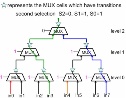
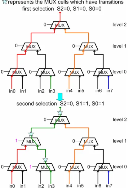
If this 8-to-1 MUX tree is used to select data, transitions of the 8-to-1 MUX tree are as follows. The first selection is set to 0 for S2, S1, and S0 shown in Figure 2. Output data of the MUX tree is in0. Then S1 and S0 change to 1 in the second selection shown in Figure 3. The selection signals in the first and second level are all
changed. Although in3 is selected correctly from the MUX tree, all MUX cells in the MUX tree have transitions. Actually, transitions of MUX cells on the output signal propagation path are necessary and the others are redundant. Figure 4 shows the minimum transitions, in which in3 can be selected correctly and only three MUX cells have transitions.
Figure 2. First selection of traditional MUX trees
Figure 4. Transitions on the output signal propagation path
2.2 Independent Selection Signals
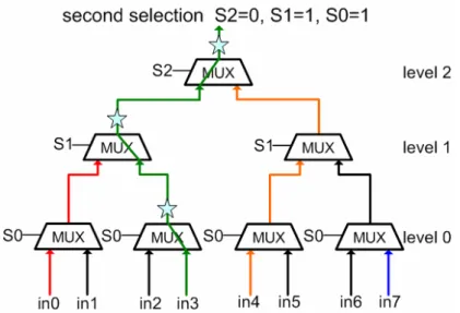
In order to achieve that only MUX cells on the output signal propagation path have transitions, the first step is to modify selection signals of the traditional MUX tree. Figure 5 shows that each MUX cell has its own selection signal. Therefore, an 8-to-1 MUX tree has seven different selection signals.
Then, this MUX tree with independent selection signals is used to select data. Take the same selections in Figure 2 and Figure 3, the first selection address is 000 and the second selection address is 011 shown in Figure 6. Because the selection signals in the same level are different, there is at most one switching selection signal in each level. In the second selection, only S01 changes to 1 in the first level and S10 changes to 1 in the second level. The other selection signals hold previous values. Thus, only three MUX cells have transitions in the second selection. Independent selection signals can minimize transitions of MUX trees.
2.3 Proposed MUX Tree Architecture
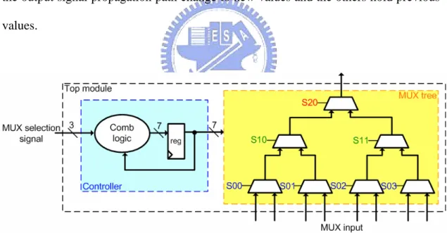
After introducing the independent selection signal control, we briefly describe how to implement it in this section. Figure 7 shows the architecture of proposed MUX tree. Controller is used to generate each selection signal of the MUX tree. Original selection signals of the MUX tree are 3 bits. When original selection signals change, Controller dynamically generates individual selection signals which are 7 bits. Controller is made up of registers and combinational logic. Registers are used to store previous values of selection signals. Combinational logic is based on the current and previous values of the selection signal to determine whether each selection signal can be updated to new values or hold previous values. Thus only the selection signals on the output signal propagation path change to new values and the others hold previous values.
Chapter 3 Proposed MUX Tree
In this chapter, two kinds of architecture are proposed to implement Controller. The first kind of architecture is the Single-Level Controller. After introducing the main idea, power ratio by the Single-Level Controller is given by the following simulation. Then analysis of power ratio is presented. According to analysis, the Two-Level Controller is proposed for improvement.
3.1 Single-Level Controller
Single-Level Controller decides that each selection signal can be updated to new values or hold previous values. The policy is that selection signals in a level are determined by those in the higher level. Figure 8 shows Single-Level Controller for an 8-to-1 MUX tree. In Figure 8, assume the selected data is in0. Operations of S00, S10, and S20 are explained as follows. Original selection signals are 3 bits and named mux_sel. Because S20 is in the highest level, it directly connects to mux_sel[2], the most significant bit (MSB) of original selection signals. S20 is updated per cycle with transitions of mux_sel[2]. S10 is in the second level so it is determined by the selection signal in the third level. S10 changes to mux_sel[1] if mux_sel[2] is zero. Otherwise S10 keeps the previous value which is stored in the register. S00 is in the lowest level so it only becomes mux_sel[0] when both mux_sel[2] and mux_sel[1] are zero.
Figure 8. Architecture of Single-Level Controller
3.2 Single-Level Controller with Resource Sharing
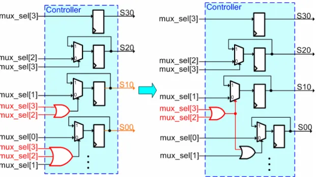
When the size of the MUX tree is large, combinational logic in the low level become complex. Figure 9 shows parts of Single-Level Controller for a 16-to-1 MUX tree. Observe the operations of S10 and S00. Both S10 and S00 have OR operations of mux_sel[3] and mux_sel[2]. These OR operations are the same and can be shared. Therefore, combinational logic can be reduced by sharing operations.
3.3 Experimental Results with Single-Level Controller
According to the main idea introduced in previous sections, the experimental results of the proposed MUX tree are presented in the following section. After simulation, power ratio for any size of MUX trees is given.
3.3.1 Experimental Environment
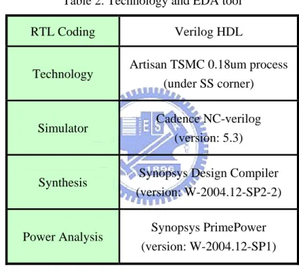
First, Table 2 gives the simple description of the experimental environment.
Table 2. Technology and EDA tool RTL Coding Verilog HDL
Technology Artisan TSMC 0.18um process (under SS corner) Simulator Cadence NC-verilog
(version: 5.3) Synthesis Synopsys Design Compiler
(version: W-2004.12-SP2-2) Power Analysis Synopsys PrimePower
(version: W-2004.12-SP1)
Then the simulation environment is described. During synthesis, it must be sure that the MUX tree module is composed of 2-to-1 MUX cells not other cells in the standard cell library. So the MUX tree is implemented by MX2X1, the MUX cell in the TSMC018 library. In order to avoid that the synthesis tool restructures the MUX tree, the command “set_dont_touch” is used. During the simulation, input data is generated randomly. Testbench generates random selection signals and input data per cycle. Besides, the maximum limitation of dumped files in the workstation and
simulation efficiency must be considered. The simulation cycle is set up 64×N and N is the number of input data. Thus it can be sure that each input data has been selected and the size of dumped files does not exceed the upper bound of the workstation. Architecture of the traditional MUX tree is shown in Figure 10. MUX selection signals have no operations and directly connect to the selection signal of each MUX cell. In the next section, power consumption of traditional MUX trees is compared with that of proposed MUX trees.
Figure 10. Architecture of the traditional MUX tree
3.3.2 Experimental Results for Single-Level Controller
After introducing the experimental environment, the simulation results are shown in this section. The simulation results are normalized by the following formula:
tree MUX al tradition of n consumptio power tree MUX proposed of n consumptio power ratio power = (1)
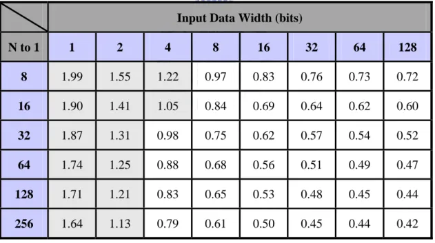
After normalization, power ratio of proposed MUX trees is shown in Table 3. In Table 3, the column represents input data width of the MUX tree and the row represents the size of the MUX tree. N is the number of input data. There are two colored blocks in Table 3. One is the gray block and the other is the white block. The gray block means that our proposed MUX tree consumes more power than the
traditional MUX tree. Therefore, the value of power ratio in the gray block is greater than 1. The white block implies that our proposed MUX tree saves power and the value of power ratio is smaller than 1. It is obvious that the gray blocks are all in the left side of Table 3. Our proposed MUX tree consumes more power than the traditional MUX tree when input data width is small. As input data width increases, power ratio of our proposed MUX tree decreases. If N, the number of input data, increases, it means that more MUX cells are needed and more transitions of MUX cells are minimized by Single-Level Controller. For the 256-to-1 MUX tree with 128-bit width input data, power saving of our proposed MUX tree is 58%.
Table 3. Power ratio by Single-Level Controller
Input Data Width (bits)
N to 1 1 2 4 8 16 32 64 128 8 1.99 1.55 1.22 0.97 0.83 0.76 0.73 0.72 16 1.90 1.41 1.05 0.84 0.69 0.64 0.62 0.60 32 1.87 1.31 0.98 0.75 0.62 0.57 0.54 0.52 64 1.74 1.25 0.88 0.68 0.56 0.51 0.49 0.47 128 1.71 1.21 0.83 0.65 0.53 0.48 0.45 0.44 256 1.64 1.13 0.79 0.61 0.50 0.45 0.44 0.42
3.3.3 Power Analysis
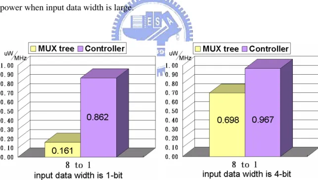
The reason why gray blocks are all in the left side of Table 3 is discussed in this section. The necessary step is to identify power dissipation of the proposed MUX tree. Our proposed MUX tree contains two modules. One is the Controller and the other is the MUX tree. Thus, power consumption of the MUX tree and Controller is dumped
during the simulation. Two MUX trees with the same size but different data width are shown in the following figures. Figure 11 shows an 8-to-1 MUX tree and input data width is 1-bit. Figure 12 also shows an 8-to-1 MUX tree but input data width is 4-bit. In Figure 11, power dissipation of the MUX tree is 0.161uW/HMz and power dissipation of Controller is 0.862uW/HMz. Additional power which is consumed by Controller is higher than power saving of the MUX tree. So our proposed MUX tree consumes more power than the traditional MUX tree. With the wider input data width, power consumption of Controller increases little but power consumption of the MUX tree increases much. It is shown in Figure 12. As the input data width increases, power saving of the MUX tree can be greater than additional power which is consumed by Controller. It is the reason why our proposed MUX tree would save power when input data width is large.
Figure 11. Power dissipation 1 Figure 12. Power dissipation 2
After analyzing power dissipation of the MUX tree and Controller, Table 4 shows the percentage of power consumption between the MUX tree and Controller. It is easier to observe the power distribution with increase of input data width. If input data
width is small, Controller occupies most of total power. As input data increases, the percentage of the MUX tree also increases. Our proposed MUX tree does not consume lower power than the traditional MUX tree until the percentage of Controller and the MUX tree is almost the same. Thus, the power ratio becomes less than 1 when input data width is 4-bit. If input data width is 128-bit, Controller only occupies few percentages of total power. So our proposed MUX tree can save much power.
Table 4. Percentage of power consumption
3.4 Two-Level Controller
From Section 3.3.3, it is concluded that reducing power consumption of Controller can let our proposed MUX tree save more power. How to reduce power dissipation of Controller is the main issue in this section.
3.4.1 Power Consumption of Registers in Controller
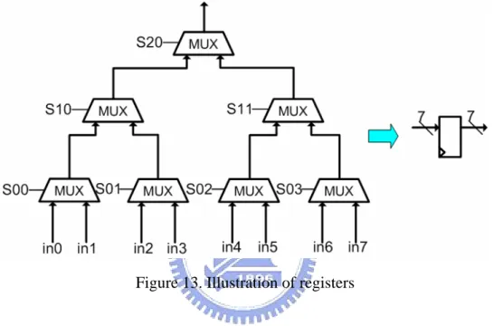
Controller is composed of registers and combinational logic. Consider power consumption of registers in Controller. Figure 13 shows that Controller has 7-bit registers. These registers are written data per cycle but not all registers need to be updated their values.
Figure 13. Illustration of registers
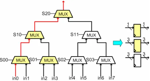
Figure 14 shows that in0 is selected from the 8-to-1 MUX tree and the output signal propagation path is in the left half. According to the location of registers, registers can be grouped into two parts. One part of registers which store the selection signals in the right half is colored white. Also the other part of registers in the left half is colored yellow. In Figure 14, yellow blocks imply that the registers need to be updated. White blocks represent that the registers do not need to be updated their values. The register which stores the selection signal in the highest level is independent. It is also colored yellow because this register is written data every cycle. Actually, power consumption of registers colored white can be reduced.
Figure 14. Registers separation
3.4.2 Intensive Clock Gating
In Section 3.4.1, it is known that all registers in Controller are written data per cycle. Although registers have no transitions, they are still written data. In this section, clock gating is used to reduce power of these registers shown in Figure 15. Generally, synthesis tool uses a multiplexer to hold the previous value of the register. Although the register holds the previous value, it is still written data and consumes power. During synthesis, the technology of clock gating is used and then the multiplexer is replaced by the clock gating (CG) cell. If the register does not update its value, the CG cell can disable clock of the register. Thus, the register is not written data and power consumption can be reduced. Consider a 32-to-1 MUX tree shown in Figure 16. The yellow MUX block represents an 8-to-1 MUX tree so there are four yellow MUX blocks in Figure 16. Registers in the 32-to-1 MUX tree are grouped into four parts and each part has 7-bit registers with clock gating. Registers which store selection signals in the high level are independent so they are not used clock gating. When the MUX tree is used to select data, only one group of registers can be enabled.
Originally, there are 31-bit transitions of registers. After intensive clock gating, there are only 10-bit transitions of registers.
Figure 15. Technology of clock gating
Figure 16. Clock gating for 32-to-1 MUX tree
3.4.3 Two-Level Controller
The technology of clock gating not only reduces power consumption of registers, bus also separates Controller into two levels. Figure 17 shows Level-1 Controller
which principally controls selection signals in the high level. Operations of selection signals in Level-1 Controller are the same as those in Single-Level Controller.
Figure 17. Level-1 Controller
Figure 18 shows Level-2 Controller which controls selection signals in the low level. In Level-2 Controller, the technology of clock gating is used. The MUX tree in Figure 18 is a leaf of the 32-to-1 MUX tree and there are 7-bit registers. The 7-bit registers are not written data until this leaf is on the output signal propagation path. In other words, that both mux_sel[4] and mux_sel[3] are equal to zero can enable the CG cell in Level-2 Controller. Additionally, combinational logic in Level-2 Controller are fewer than those in Single-Level Controller. For example, S20 is determined by selection signals in the fourth and fifth level in Single-Level Controller. In Level-2 Controller, S20 has no operations and is directly connected to the selection signal in the third level.
Figure 18. Level-2 Controller
3.4.4 Bit-widths of Clock Gating Registers
The bit-width of clock-gating registers is discussed in this section. Figure 19 shows an 8-to-1 MUX tree and the minimum bit-width of clock gating registers is 3-bit. The simulation results are shown in Table 5. The proposed MUX tree with clock gating consumes more power than that without clock gating. So the minimum bit-width of clock gating registers is 7-bit. If the bit-width of grouping registers is smaller than 7-bit, like an 8-to-1 MUX tree, the technology of clock gating is not used.
Table 5. Simulation results of minimum bit-widths
Input Data Width (bits)
Technology 1 2 4 8 16 32 64 128
Clock
Gating 2.14 1.63 1.26 1.01 0.83 0.76 0.73 0.72
Non-Clock
Gating 1.99 1.51 1.22 0.97 0.83 0.76 0.73 0.72
Figure 19. Minimum bit-widths of clock gating registers
After deciding the minimum bit-width of clock gating registers, the maximum bit-width of clock gating registers is given. The maximum bit-width of clock gating registers is set by the following formula:
2S-2-1 for N<256
2S-3-1 for N=256 (2) S in the formula (2) is the bit-width of selection signals. By this formula, clock gating registers of MUX trees can be grouped into four or eight parts. Figure 20 is an example for a 64-to-1 MUX tree. S is equal to 6 and N is equivalent to 64. So the maximum bit-width of clock gating registers is 15-bit. Clock gating registers are grouped into four parts and each part is represented by a yellow MUX block which is a 16-to-1 MUX tree. With operations of the 64-to-1 MUX tree, there are only 18-bit transitions of registers.
Figure 20. Maximum bit-widths of clock gating registers
It is necessary to discuss why the maximum bit-width of clock gating registers is not set by the formula, 2S-3-1. Figure 21 shows the 64-to-1 MUX tree with 8 groups of clock gating registers. Each group is represented by a yellow MUX block which is an 8-to-1 MUX tree. The maximum bit-width of clock gating registers is set by the formula, 2S-3-1. So it is 7-bit. Total transitions of registers are 14-bit.
Compare power consumption of these two different grouping. Different grouping has an influence on power consumption of registers, CG cells, and combinational logic. Power consumption of registers has been presented. Consider a 64-to-1 MUX tree. Transitions of registers are 18 bits for 4 groups and 14 bits for 8 groups. Then, comparison of combinational logic and CG cells is shown in Figure 22 and Figure 23. Combinational logic of Level-1 Controller with 4 groups is almost the same as that with 8 groups. Combinational logic of Level-2 Controller with 4 groups is more complex than that with 8 groups. So Controller with 8 groups has less combinational logic. Besides, Controller with 8 groups has 8 CG cells and Controller with 4 groups only has 4 CG cells. There are more operations of enable signals for CG cells in Controller with 8 groups. Therefore, CG cells consume less power in Controller with 4 groups.
Power comparison of different grouping is concluded in Table 6. Controller with 8 groups has fewer transitions of registers and less combinational logic. But CG cells of Controller with 4 groups consume less power. For Controller with 8 groups, power consumption of registers and combinational logic decreases but power consumption of CG cells increases as the size of the MUX tree increases. It can be based on simulation results to determine that Controller with 8 groups is better or not.
Table 6. Power comparison of different grouping 4 groups 8 groups transitions of registers 1+1+1+(2S-2-1) 1+3+3+(2S-3-1)
the number of CG cells 4 8 combinational logic more less
Figure 22. Operation comparison for Level-1 Controller
Table 7 shows the simulation results of these two different grouping. Controller with 4 groups consumes less power than Controller with 8 groups. It is because decrease power of registers and combinational logic is less than increase power of CG cells. If the size of the MUX tree is 64, Controller with 4 groups is better.
Table 7. Power comparison for 64-to-1 MUX tree
Input Data Width (bits)
Technology 1 2 4 8 16 32 64 128
4 groups 1.41 1.05 0.77 0.64 0.53 0.50 0.48 0.46
8 groups 1.50 1.10 0.80 0.65 0.54 0.50 0.48 0.46
64-to-1 MUX tree
Another simulation result is shown in Table 8. Power consumption of Controller with 4 groups and 8 groups is almost the same for the 128-to-1 MUX tree. It implies that decrease power of registers and combinational logic is almost the same as increase power of CG cells. If the size of the MUX tree increases more, increase power of CG cells is higher than decrease power of registers and combinational logic. Therefore, Controller with 8 groups is better for the 256-to-1 MUX tree. The simulation results are shown in Table 9. It is the reason why the maximum bit-width of clock gating registers is set by formula (2).
Table 8. Power comparison for 128-to-1 MUX tree
Input Data Width (bits)
Technology 1 2 4 8 16 32 64 128
4 groups 1.25 0.93 0.69 0.58 0.49 0.46 0.44 0.44
8 groups 1.24 0.93 0.69 0.58 0.49 0.46 0.45 0.44
128-to-1 MUX tree
Table 9. Power comparison for 256-to-1 MUX tree
Input Data Width (bits)
Technology 1 2 4 8 16 32 64 128
4 groups 1.09 0.81 0.64 0.55 0.46 0.43 0.43 0.42
8 groups 1.04 0.79 0.61 0.53 0.46 0.43 0.43 0.42
256-to-1 MUX tree
3.5 Experimental Results with Two-Level Controller
Before looking at the simulation results, the advantage of Two-Level Controller is introduced first. Technology of clock gating is not only used to reduce power consumption of registers in Controller but also separated Controller into two levels. Level-2 Controller has less combinational logic than Single-Level Controller. So power consumption of combinational logic can be reduced. It implies that power consumption of Controller is reduced and our proposed MUX tree can save more power.
Table 10. Power ratio by Single-Level Controller
Input Data Width (bits)
N to 1 1 2 4 8 16 32 64 128 8 1.99 1.55 1.22 0.97 0.83 0.76 0.73 0.72 16 1.90 1.41 1.05 0.84 0.69 0.64 0.62 0.60 32 1.87 1.31 0.98 0.75 0.62 0.57 0.54 0.52 64 1.74 1.25 0.88 0.68 0.56 0.51 0.49 0.47 128 1.71 1.21 0.83 0.65 0.53 0.48 0.45 0.44 256 1.64 1.13 0.79 0.61 0.50 0.45 0.44 0.42
Table 11. Power ratio by Two-Level Controller
Input Data Width (bits)
N to 1 1 2 4 8 16 32 64 128 8 1.99 1.55 1.22 0.97 0.83 0.76 0.73 0.72 16 1.88 1.39 1.03 0.84 0.68 0.64 0.62 0.59 32 1.66 1.18 0.90 0.71 0.60 0.56 0.53 0.51 64 1.41 1.05 0.77 0.64 0.53 0.50 0.48 0.46 128 1.25 0.93 0.69 0.58 0.49 0.46 0.44 0.44 256 1.04 0.79 0.61 0.53 0.46 0.43 0.43 0.42
Table 11 is power ratio by Two-Level Controller. Table 10 is power ratio by Single-Level Controller and it is the same as Table 3. It is duplicated here in order to compare with power ratio by Two-Level Controller conveniently. For the 8-to-1 MUX tree, power ratio by Two-Level Controller is the same as that by Single-Level
Controller. Because the 8-to-1 MUX tree is not satisfied with the minimum bit-width of clock gating, architecture of Two-Level Controller is like that of Single-Level Controller. For the other sizes of MUX trees, power saving by Two-Level Controller is greater than that by Single-Level Controller. Besides, the number of gray blocks in Table 11 is less than that in Table 10. With wider input data width, power saving by Two-Level Controller is almost the same as that by Single-Level Controller. It is because the MUX tree occupies most of total power consumption. Therefore, Controller has few influences on total power consumption. Reducing power consumption of Controller does not affect total power saving much when input data width is large.
Chapter 4 Experimental Results and Analysis
After introducing the main idea and experimental results in the previous chapter, power ratio is analyzed in this chapter. When the MUX tree become large, power ratio decreases slowly and does not continue to go down. In this chapter, the reason why power consumption of proposed MUX tree cannot be reduced infinitely is presented.
4.1 Transitions of MUX Cells
In this section, the first necessary step is to discuss transitions of MUX cells. Consider a 2-to-1 MUX cell shown in Figure 24. There are two kinds of inputs in MUX cell. One is input data and the other is the selection signal. Either one has an effect upon the output transition. Therefore, there are two factors which affect the output transitions of the MUX cell. One is switching activity of input data and the other is switching activity of selection signals.
Figure 24. 2-to-1 MUX cell
In Figure 25, the selection signal is the same between the first selection and the second selection. Although the selection signal holds the previous value, input data changes from 0 to 1 during the second selection. Therefore, the MUX cell still has transitions because of input data switching.
Figure 25. Fixed the selection signal but unfixed input data
Figure 26 shows that all MUX cells in the MUX tree have transitions with input data switching. The first selection is the same as the second selection but input data changes in the second selection. Input data switching causes that all MUX cells have transitions in the second selection. Selection signals are fixed in our proposed MUX tree but input data is not fixed. Therefore, input data switching is the main reason why power consumption of our proposed MUX tree cannot be reduced infinitely.
4.2 Constrained Input Data
In this section, low switching activity of input data is given to discuss how much power our proposed MUX tree can save. Actually, there are some applications for MUX trees which satisfy low switching activity of input data. The application for register file is a suitable example. Figure 27Figure 27 shows a single-write-port register file. The MUX tree is used to select data from the register file. Only one register entry would be written data per cycle. Most input data of the MUX tree hold previous values and only one of input data changes. Therefore, testbench would simulate like this single-write-port register file during the simulation. The simulation environment describes in Section 3.3. Most experimental setups are the same as those in Section 3.3.
Figure 27. Single-write-port register file
4.3 Experimental Results
After constraining input data, simulation results are shown in this section. Table 12 shows power ratio by Single-Level Controller and the random simulation environment is used. Table 13 also shows power ratio by Single-Level Controller but testbench simulates like a single-write-port register file. The distribution of power ratio in Table 12 and Table 13 is the same. In the right side of the table, power ratio is smaller than
1. In the left side of the table, power ratio is greater than 1 and it implies that our proposed MUX tree consumes more power than the traditional MUX tree. There are no saturation problems in Table 13. Power consumption of our proposed MUX tree can decrease as input data width increases. If our proposed MUX tree is applied for single-write-port register files, power saving can be up to 93% for 256-to-1 MUX tree with 128-bit width input data. Table 14 and Table 15 shows power ratio by Two-Level Controller. The former is simulated in random environment and the latter is simulated with constrained input data. In Table 15, power saving has no saturation problems. Power saving by Two-Level Controller is also 93% for 256-to-1 MUX tree with 128-bit width input data.
Table 12. Single-Level Controller simulated in random environment
Input Data Width (bits)
N to 1 1 2 4 8 16 32 64 128 8 1.99 1.55 1.22 0.97 0.83 0.76 0.73 0.72 16 1.90 1.41 1.05 0.84 0.69 0.64 0.62 0.60 32 1.87 1.31 0.98 0.75 0.62 0.57 0.54 0.52 64 1.74 1.25 0.88 0.68 0.56 0.51 0.49 0.47 128 1.71 1.21 0.83 0.65 0.53 0.48 0.45 0.44 256 1.64 1.13 0.79 0.61 0.50 0.45 0.44 0.42
Table 13. Single-Level Controller simulated with constrained input data
Input Data Width (bits)
N to 1 1 2 4 8 16 32 64 128 8 2.19 1.73 1.31 1 0.76 0.64 0.59 0.56 16 2.11 1.54 1.06 0.77 0.54 0.44 0.41 0.37 32 2.12 1.43 0.96 0.62 0.42 0.32 0.28 0.24 64 1.95 1.34 0.80 0.50 0.31 0.23 0.19 0.16 128 2.01 1.33 0.75 0.45 0.26 0.17 0.13 0.11 256 1.89 1.20 0.68 0.39 0.22 0.13 0.10 0.07
Table 14. Two-Level Controller simulated in random environment
Input Data Width (bits)
N to 1 1 2 4 8 16 32 64 128 8 1.99 1.55 1.22 0.97 0.83 0.76 0.73 0.72 16 1.88 1.39 1.03 0.84 0.68 0.64 0.62 0.59 32 1.66 1.18 0.90 0.71 0.60 0.56 0.53 0.51 64 1.41 1.05 0.77 0.64 0.53 0.50 0.48 0.46 128 1.25 0.93 0.69 0.58 0.49 0.46 0.44 0.44 256 1.04 0.79 0.61 0.53 0.46 0.43 0.43 0.42
Table 15. Two-Level Controller simulated with constrained input data
Input Data Width (bits)
N to 1 1 2 4 8 16 32 64 128 8 2.19 1.73 1.31 1 0.76 0.64 0.59 0.56 16 2.08 1.53 1.04 0.78 0.54 0.43 0.40 0.37 32 1.84 1.25 0.85 0.58 0.39 0.30 0.26 0.23 64 1.50 1.05 0.63 0.43 0.27 0.20 0.18 0.15 128 1.36 0.91 0.52 0.35 0.20 0.14 0.12 0.10 256 1.05 0.68 0.40 0.26 0.15 0.10 0.08 0.07
Chapter 5 Conclusions and Future Works
In this thesis, the architecture of low power MUX tree is proposed. The first step is to let each MUX cell have its own selection signals. Then Controller can be based on the current and previous selection signals to generate individual selection signals of MUX cells dynamically. Controller lets most of selection signals hold previous values. Thus redundant transitions of MUX cells in the MUX tree can be minimized. According to the experiment results, our proposed MUX tree can save power as input data width increases. For the 256-to-1 MUX tree and 128-bit width input data, power saving of the proposed MUX tree is 58% in the worst case, such as the random simulation. Power saving can be up to 93% in the best case, such as constrained input data. So it can be concluded that power saving of the proposed MUX tree is between 93% and 58% in typical case.
In this thesis, the size of the MUX tree is always the power of 2. However, the number of MUX cells in each level is unbalanced for any n-to-1 MUX tree where n is not the power of 2. For this unbalanced MUX tree, power saving depends on the test patterns. It can be expected that the proposed MUX tree saves more power if the unbalanced path is selected frequently. In future works, we shall prove our point.
References
[1] Deming Chen and Jason Cong, “Register Binding and Port Assignment for Multiplexer Optimization,” Design Automation Conference, 2004. Proceedings of the ASP-DAC 2004. Asia and South Pacific, Page(s):68 – 73, Jan. 2004.
[2] Deming Chen, Jason Cong, and Yiping Fan, “Low-Power High-Level Synthesis for FPGA Architectures,” Low Power Electronics and Design, 2003. ISLPED '03. Proceedings of the 2003 International Symposium on, Page(s):134 – 139, Aug. 2003.
[3] L.E.M. Brackenbury and W. Shao , “Lowering power in an experimental RISC processor,” Microprocessors and microsystems [0141-9331] Brackenbury yr:2007 vol:31 iss:5 pg:360,January 2007.
[4] Caldari, M.; Conti, M.; Coppola, M.; Crippa, P.; Orcioni, S.; Pieralisi, L.; Turchetti, C.; “System-Level Power Analysis Methodology Applied to the AMBA AHB Bus,” Design, Automation and Test in Europe Conference and Exhibition, 2003, Page(s):32-37 suppl, 2003.
[5] U. Narayanan, H. W. Leong, K.-S. Chaung, and C. L. Liu, “Low power multiplexer decomposition,” Proceedings of International Symposium on Low Power Electronics Design, pp. 269-274. 1997.
[6] Hsiao-En Chang, Juinn-Dar Huang, and Chia-I Chen, "Input Selection Encoding for Low Power Multiplexer Tree," IEEE Int'l Symp. on VLSI Design, Automation, and Test, pp. 228-231, Apr. 2007.
[7] K. Kim, T. Ahn, S.-Y. Han, C.-S. Kim, and K.-H. Kim, “Lowpower multiplexer decomposition by suppressing propagation of signal transitions,” IEEE Int’l Symp. on Circuits and Systems, vol. 5, pp 85-88, 2001.
[8] Sebastian T. Ventrone, “Low power multiplexer circuit,” United States Patent, Patent Number:6,054,877, Apr.2000.
[9] Douseki, T. and Ohmori, Y. “BiCMOS circuit technology for a high-speed SRAM,” IEEE journal of solid-state circuits, vol:23,iss:1,pg:68, Feb. 1988.