國 立 交 通 大 學
電子工程學系電子研究所
碩 士 論 文
奈米級金氧半場效電晶體之通道背向式散射係數萃取
Extraction of Channel Backscattering Coefficients in
Nanoscale MOSFET
研 究 生 : 周益欽 Yi-Chin Chou
指導教授 : 陳明哲 Prof. Ming-Jer Chen
奈米級金氧半場效電晶體之通道背向式散射係數萃取
Extraction of Channel Backscattering Coefficients in
Nanoscale MOSFET
研 究 生 : 周益欽 Student:Yi-Chin Chou
指導教授 : 陳明哲 Advisor:Prof. Ming-Jer Chen
國 立 交 通 大 學
電子工程學系 電子研究所碩士班
碩 士 論 文
A ThesisSubmitted to Department of Electronics Engineering & Institute of Electronics
College of Electrical Engineering and Computer Science National Chiao Tung University
in Partial Fulfillment of the Requirements for the Degree of
Master of Science in
Electronic Engineering June 2004
Hsinchu, Taiwan, Republic of China
奈米級金氧半場效電晶體之通道背向式散射係數萃取
研究生:周益欽 指導教授:陳明哲博士
國立交通大學
電子工程學系電子研究所
摘要
閘極氧化層厚度為 1.65 奈米的 N-型通道金氧半電晶體,在靠近源極的kBT layer 內 之通道背向式散射係數被分為兩個要素探討:背向式散射在半熱平衡狀態下的平均 自由路徑,以及 kBT layer 的寬度。另外確認此分離方法正確性的證據也更進一步 提出:(i) 靠近源極的導帶概觀圖; (ii) 另一個透過跟溫度有關的汲極電流公式來 求得背向式散射係數的方法。這些發現彼此之間更具有相當的一致性,並支持著背 向式散射確實是此係數的起源。因此,我們可以合理的宣稱:這些被分離的要素, 以及相對應與溫度及偏壓的關係,可以被適宜地用以描述在通道背向式散射理論架 構之下運作的元件操作情形。Extraction of Channel Backscattering Coefficients in
Nanoscale MOSFET
Student: Yi-Chin Chou Advisor:Dr. Ming-Jer Chen
Department of Electronics Engineering
Institute of Electronics
National Chiao Tung University
Abstract
Abstract:
Channel backscattering coefficients in the kBT layer (near the source) of 1.65-nm
thick gate oxide n-channel MOSFETs are systematically separated into two distinct components: the quasi-thermal-equilibrium mean-free-path for backscattering and the width of the kBT layer. Evidence to confirm the validity of the separation procedure is
further produced: (i) the near-source channel conduction-band profile; and (ii) an analytic temperature-dependent drain current model for the channel backscattering coefficients. The findings are also consistent with each other and therefore corroborate channel backscattering as the origin of the coefficients. Consequently, it can be reasonably claimed that the separated components, as well as their dependencies on temperature and bias, are adequate while being used to describe the operation of the devices undertaken within the framework of the channel backscattering theory.
致謝
碩士兩年的時光,過得比想像中快許多,也過得比想像中快樂充實,這實在要 感謝很多人的幫忙。 首先要感謝,也最感謝的是陳明哲教授。在研究生兩年的經驗及聽聞中,我慢 慢的體會到,沒有最好的指導教授,只有最適合你的指導教授;而老師便是我各方面 都相當投契指導教授。不管是做學問時,遇到困難時的點子,舊有東西做新發揮的創 意;投論文時一絲不苟的嚴謹;閒聊時對研究對人事的態度;請假爬山時的欣然應許。 在此雖然紙短,但實在衷心的希望能表達對老師的感謝。 研究生的幸福取決於老師跟實驗室,我們人少但感情融洽的實驗室是這快樂兩 年不可或缺的因素。大師兄卓煜盛教我軟體使用;二師兄呂明霈指導我諸多疑問並教 我量測;林大文學長做人做事認真的態度;李亨元的戰友情誼;陳榮挺超時守護實驗 室的督促;林盈秀的美食資訊。少了這些我的碩士生涯是不可能圓滿的。 跨過碩士這個階段,仍然持續陪著我的家人與朋友們,我也要感謝你們。感謝 你們的關心與幫助,讓我保有一點研究之外的生活。最後我要感謝女友耀璇,你認真 且勇敢的人生態度一直鼓勵著我。 謹以此微不足道的感言獻給每一位我認識的人,感謝你們。Contents
Abstract (Chinese)………...i
Abstract (English)………...ii
Acknowledgement………..iii
Contents………..…iv
Figure Captions………...v
Chapter 1 Introduction………...1
Chapter 2 I-V Fitting Methodology………...…4
2-1 Theory…………..………...4
2-2 Devices under Study……….…7
2-3 Parameter Extraction………7
2-4 Results……….13
Chapter 3 Temperature-dependent Method………15
3-1 Model Description………...…15
3-2 Experiment………..16
3-3 Results……….…17
Chapter 4 Discussion and Interpretation………18
Chapter 5 Conclusion……….20
Figure Captions
Fig. 1 Schematic diagram of channel backscattering theory in high drain voltage region. F is the incident flux source and rC is the channel backscattering coefficient. l is the critical length over kT potential drop.
Fig. 2 The near-gate physical environment which depicts the relation between EF and Eij. Ec at the junction of gate and P-substrate is adopted as reference.
Fig. 3 A schematic flowchart summarizing the procedure of extracting rc and l.
Fig. 4 Measured capacitance compared with simulated capacitance at temperature = 25oC.
Fig. 5 Simulation results of Qinv, inversion charge versus gate voltage plot with temperature as parameter.
Fig. 6 Schematic illustration of deriving Ceff from Qinv-VGO plot.
Fig. 7 Simulation results of Vinj, injection velocity of the carriers versus gate voltage with temperature as parameter.
Fig. 8 Measured drain current versus gate voltage with temperature as parameter.
Fig. 9 Schematic demonstration of extracting Vth by Gm-max method from ID-VG plot.
Fig. 10 Schematically presented constant current method of extracting ∆Vth for DIBL.
Fig. 12 Derived λ, mean free path versus gate voltage with temperature as parameter.
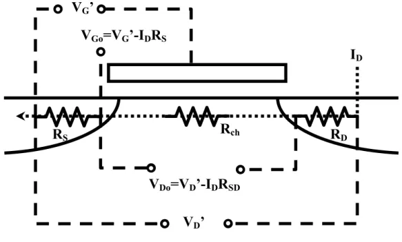
Fig. 13 Equivalent circuit of MOSFET with source and drain series resistance.
Fig. 14 Extracted RSD, source and drain series resistance of different Lmask.
Fig. 15 Extracted rc versus gate voltage at VD = 1.0V with temperature as parameter.
Fig. 16 Separated l versus at VD = 1.0V with temperature as parameter.
Fig. 17 Derived temperature-dependent power coefficients versus gate voltage at VD = 1.0V
Fig. 18 Schematically depicted procedure of fitting α.
Fig. 19 Comparison of rc between temperature-dependent and I-V fitting method for Lmask = 90nm at temperature = 25oC, VD = 1.0V.
Fig. 20 Resultant rc comparison between VD = 0.5V and VD = 1.0V at temperature = 25oC and Lmask = 90nm.
Fig. 21 Schematic illustration of near-source conduction-band energy profile. The zero point is set as the top energy of kBT layer.
Fig. 22 Corresponding rc and l versus Lmask at temperature = 25oC, VG = 1V and VD = 1V.
Chapter 1
Introduction
As MOSFET channel lengths continue to decrease with a rapid pace toward nanoscale regime, quantum mechanics is expected to govern the underlying transport details. It is generally recognized that while carriers, during the operation of the device, encounter significant space confinements and few scatterings, the conventional semiconductor transport theory would lose its accuracy in addressing such situations. To circumvent this issue, alternative researches devoted to the areas of mesoscopic physics have been proposed one after another [1]-[4]. Among them, channel backscattering theory [5],[6] has attracted increasing attention due to the potential of being able to provide a new perspective about carrier transport in nanoscale MOSFETs.
The channel backscattering theory describes a wave-like transport of carriers through the channel from source to drain. As schematically shown in Fig. 1, the channel length Leff is divided into two parts: 0 < x < l and l < x < Leff. Here l represents the critical length from the source the conduction band bends down by a thermal energy of kBT, where kB is Boltzmann’s constant and T the temperature [5],[6]. At the top of the source-channel junction barrier, the carriers are injected from the source reservoir into the channel. The height of the barrier is essential and can be modulated through applied gate voltage (VG) and drain voltage (VD). The latter is involved with well-known DIBL [5]. During above-threshold operation, the barrier still exists but gains less influence from the gate. Inside the kBT layer, a certain fraction, denoted rc, of carriers with incident flux F are reflected back to source, so this ratio being named backscattering coefficient. The resultant drain current is thus effectively a function of the extent of backscattering, as in terms of rc. Therefore, by
means of extracting rc, we could assess certain key factors such as defining the performance limits [7],[8] or evaluating the efficiency of devices by specific technology.
According to channel backscattering theory, the drain current, ID, is simply related to Qinv and vinj [5],[6]:
) 1 ( ) 1 ( C C inj inv D r r υ Q I + − = (1)
, where Qinv is the inversion layer charge density per unit area at the top of the source-channel junction barrier and is composed of both injected and reflected flux; and vinj is the thermal injection velocity. Here the term Qinv/(1+rc) could be considered as the carriers injected from source and (1-rc) the ratio of carriers traveling across the barrier to drain. With this relationship, assessment of rc has been proposed by I-V fitting method [7],[10],[11]. Furthermore, another temperature dependent method [9] developed recently is introduced as a new way to explore the device.
It is worthy to notice that through multiple backscattering events in the kBT layer, rc is related to l by [5]: l λ + = 1 1 c r (2)
where λ denotes the quasi-equilibrium mean-free-path for backscattering. The relationship implies that once we could decouple λ and l from rc, we would be able to gain physical insights into underlying mechanism.
In this thesis, the extraction of rc and the decoupling of λ and l both are performed on 1.65-nm thick gate oxide n-channel MOSFETs having physical gate
length of 68nm. First of all, a quantum mechanical simulation [12] on a MOS system furnishes values of Qinv and vinj with process parameters as input, followed by fitting of I-V to determine backscattering coefficients. The temperature dependent extraction technique is then applied to provide extra experimental evidence. The dependencies on applied bias and temperature are crucial to clarify the origin responsible. In addition, interpretations and clarifications are drawn in the way, which can substantially improve current understandings of the channel backscattering theory and its potentials.
Chapter 2
I-V Fitting Methodology
2-1 Theory
In this section, we would first explain the main formula in more detail and demonstrate the derivation of simulation parameters.
Main Formula
We are deriving the main formula from (1). Assuming operation under saturation region, the current flux in the channel could be deduced to be just that from source to channel, F, whereas that from drain to channel could be ignored. Here F can be presented as:
inj
S v
n
F = +⋅ (3)
where nS+ denotes the carrier density per unit area injecting toward +x direction into channel and vinj indicates the corresponding thermal velocity. Assuming certain ratio rc of F is backscattered within kBT layer, the reflected part toward –x direction and the transmitted part to drain could be expressed respectively by rcF and (1-rcF). Note that it is assumed that no energy loss during backscattering so both rcF and (1-rcF) move with the original velocity, vinj. At the interface between source and channel, the total carrier density per unit area, nStot(0) can therefore be obtained by:
) 1 ( ) ( 1 ) 0 ( c S c inj S F rF n r v n tot = ⋅ + = ⋅ + + (4)
= (1-rc)F and the MOS electrostatic equation of inversion layer charge density is [5]: ) ( ) 0 ( G th eff S V V q C n tot = − (5)
then we can derive:
c c inj th G eff S c c inj S c inj inj drain D r r v V V C W n r r v q W n r v q W v n q W I tot sat + − ⋅ − ⋅ = + − ⋅ ⋅ ⋅ = − ⋅ ⋅ ⋅ = ⋅ ⋅ ⋅ = + 1 1 ) ( 1 1 ) 1 ( ) 0 ( (6)
Derivations of simulation parameters
In (6), the terms Ceff and vinj could not be directly assessed by experimental data; so, to circumvent it, alternative methods are necessary such as temperature-dependent method [9] discussed later and the theoretical calculation via quantum mechanical simulation [8],[12], which is to be discussed in this chapter.
The one-dimensional quantum mechanical simulation [13],[14] dedicated to an n+ polysilicon/gate oxide/p-type substrate MOS system is initiated by setting a distinct physical environment through three significant process parameters: Tox, Nsub, and Npoly. Here Tox is the thickness of gate oxide and Nsub and Npoly are the doping concentration in substrate and in polysilicon, respectively.
With a distinct physical environment set up as shown in Fig. 2, the Fermi level, EF, and subband energy levels, Eij, can be subsequently derived by [14]:
) ( s bn
F q
3 / 2 3 / 1 2 ) 2 ) 4 1 ( 3 ( ) 2 ( − = qF i m E Si Zj ij π h (8)
In (8), i represents subband index; j the valley index being 1 for two-fold valley or 2 for 4-fold valley; mZj the corresponding normal electron effective mass in the jth valley; and the most important parameter, FSi, the silicon surface electric field, is solved by an iteration procedure [14].
EF and Eij together characterize a specific MOS system. Once they can be determined, a series of parameters leading to Ceff and vinj can immediately be quantified. At first, the charge density associated with subband i for specific valley is
)] exp( 1 [ 2 2 k T E E n T k m n B i F B di i s − + = l h π γ (9)
where γ denotes the valley degeneracy; mci the density-of-states effective mass for subband i. (9) could be further interpreted in two aspects: one for Ceff and the other for vinj. The charge density in underlying 2DEG (two-dimensional electron gas) inversion layer, Qinv, could be obtained by summing all nsi for correspondent subband i and valley j so as to assess Ceff by fitting MOS electrostatics formula Qinv = Ceff(VGO - Vtho). On the other hand, for each distinct subband i, the thermal injection velocity is [8]: )] exp( 1 [ ) ( 2 1/2 2 T k E E n T k E E m Tm k v B i F B i F di ci B i inj − + − ℑ = l π (10)
integral of order one-half. Finally, the effective thermal injection velocity at the top of the source-channel junction barrier is defines as [8]:
∑
∑
= i s i inj i s inj n υ n υ (11)In 2DEG MOS system, the effective mass is separated into two sorts due to the z-direction confinement: the longitudinal mass ml = 0.916mo and the transverse mass mt = 0.19mo, where mo means the original electron mass. This thus causes further difference in conductivity effective mass, mci and density-of-states effective mass mdi: mci = mt and mdi = mt for 2-fold valleys and mci = 2mlmt/(ml + mt) and mdi = (mlmt)0.5.
2-2 Devices under Study
Halo-implanted bulk n-channel MOSFETs under investigation were fabricated in state-of-the-art manufacturing process. Tox = 1.65 nm; channel width, W = 10μm; and mask gate length, Lmask from 10μm to 0.075μm. The main extraction procedure would be demonstrated on Lmask = 0.09μm. As for the measure conditions, we adopt the following systems: HP4156B and a thermal chuck and cooling system to set up the conditions: VG = 0.1~1.2V; VD = 0.025, 0.1, 0.5, and 1.0V; and temperature = -40oC, -10oC, and 25oC.
2-3 Parameter Extraction
Flowchart
Fig. 3 summarizes schematically the procedure of extracting rc and l. The round-corner frames indicate the experiment data; the indented-corner frames imply the extraction and simulation data; and the connection lines illustrate the relationship
between the data and how to derive them in series. We would then demonstrate the extraction procedure step by step based on the connection lines of the flowchart.
C-V curve
The C-V measurement is performed on 50μm×50μm testkey. Fig. 3 shows experimental results of capacitance with unit inμF/cm2.
T
ox, N
sub, N
polyAs shown in Fig. 3, Tox, Nsub, and Npoly are obtained by C-V comparison. The measured C-V curve is compared with that calculated by the quantum simulator with Tox, Nsub, and Npoly as input. Since Tox, Nsub, and Npoly separately affect the C-V curve in different ways, a distinct set of Tox, Nsub, and Npoly can be found with optimum C-V match. In Fig. 4, we get Tox = 1.65 nm, Nsub = 8×1017 cm-3 and Npoly = 9×1019 cm-3
Q
inv, v
inj, C
effWith Tox, Nsub, and Npoly known, Qinv, vinj, and Ceff can be directly assessed by the simulator. Fig. 5 shows the resulting inversion charge, Qinv, versus gate voltage under T = -40oC, -10oC and 25oC. Furthermore, C
eff fitted by one-dimensional MOS electrostatics formula Qinv = Ceff(VGO-Vtho) is depicted in Fig. 6. The corresponding vinj is given in Fig. 7.
I
D-V
GThe drain current-gate voltage, ID-VG curve is measured under temperature = -40oC, -10oC, and 25oC with Lmask = 90nm as shown in Fig. 8. It is worthy noticing that the curves of different temperature intersect each other at a critical gate voltage around VG = 0.45V as mentioned in [9]. Besides, ID-VG is also measured with drain voltage VD as parameter. The results are shown in Fig. 9 in order to compensate the
insufficiency of the 2DEG quantum simulator concerning the effect of VD.
V
ththreshold voltage
In order to circumvent potential uncertainties such as DIBL in determining threshold voltage of nanoscale devices, we adopt a two-step method.
First, Vtho, the threshold voltage under low VD (25mV) is extracted by maximum-transconductance method at T = -40oC, -10oC, and 25oC. Fig. 9 shows a typical procedure of extracting Vtho. Initially ID is differentiated with respect to VD and the maximum transconductance, Gm-max is then picked up. Next, we draw a tangent line which intersects the ID-VG curve at the corresponding Gm-max point. The intersection of this tangent line with the VG-axis determines Vtho.
Second, on the purpose of incorporating DIBL effect in determining threshold voltage under higher VD, the magnitude of barrier lowering which induces ΔVth is evaluated by the constant current method (CCM) as shown in Fig. 10. The specific constant current is chosen to be around (W/L)×10-7 A, in order to intersect the exponentially-growing region of drain current, leading to ∆Vth. Thus the Vth under different VD can be approximated by Vth = Vtho – ΔVth.
µ
no, mobility
We adopt a drain conductance method (Gd method) [15] to estimate the near-thermal-equilibrium mobility µno on long-channel devices. This method is initiated with the usual current-voltage relationship under very low drain bias:
D th Go eff D D th Go eff D V V V L W C V V V V L W C I ] ( ) 2 1 ) [( − − 2 ≈ ⋅ ⋅ − ⋅ ⋅ =µ µ (12)
By differentiating (12) with respect to VD we would get: ] ) [( ] ) [( V V V DIBL L W C dV dV V V V L W C dV dI D th GO eff D th D th GO eff D D =µ⋅ ⋅ ⋅ − − ⋅ =µ⋅ ⋅ ⋅ − − ⋅ (13) Finally, the near-thermal-equilibrium mobility µno is derived in the form
] ) [(V V V DIBL W C L dV dI D th GO eff D D ⋅ − − ⋅ ⋅ ⋅ = µ (14)
Fig. 11 reveals the mobility curve separated into three governing effects: Coulombic scattering, phonon scattering, and surface roughness scattering. The corresponding temperature dependencies of mobility are also consistent with our expectation.
λ, mean-free-path
The mean-free-path λ is related with µno and vinj by:
inj no B v q T k µ λ=2 (15)
Therefore, the finished extraction of µno and vinj makes it straightforward to evaluate λ as shown in Fig. 11. We could see that the λ dependency on temperature is distinctly separated into two parts: below VG = 0.45V, λ increases with increasing temperature and above VG = 0.45V, λ decreases with increasing temperature. The former effect against the usual idea that λ decreases with increasing temperature is due to thermal motion dominating over phonon scattering or surface roughness scattering. On the other hand, the individual λ-VG curve is coincident with the mobility-VG relationship. The extraction of λ value would play a significant role
later on the separation of kBT layer length, l.
I
G-V
GIG-VG curves are measured on various Lmask in linear region in order to get the corresponding gate length, LG, which would be adopted as a more precise reference when deriving RSD.
L
G, gate length
Gate length is extracted simply by the gate current ratio. On a well-fabricated wafer, the LG-Lmask plot shows a common linear relationship. The reason why LG is used as reference instead of Lmask is that LG serves as a more accurate gauge. Because certain differences do exist unavoidably when defining LG from Lmask = 10µm to 0.075µm, a more reliable LG reference is then developed to take charge of Lmask = 1.2µm to 0.075µm. That is said, IG-VG of LG = 1.2µm is now set as typical long channel length for comparison with shorter channel length to distinguish the slight deviation occurring in patterning LG.
R
SD, series resistance
As shown in Fig. 13, there exists series resistance RSD between the external terminal and the active region.. Here the drain resistance RD is reasonably assumed to be the same as source resistance RS. As a result, the internal VGo should be corrected by VGo = VG’ – IDRS. Similarly, VDo = VD’ – IDRSD.
The source-drain series resistance RSD lying between the intrinsic MOSFET and the external terminal is extracted by shift-and-ratio method [15]. It is initiated from the attempt separating the total external resistance into two parts [15]:
) ( ) ( G th SD eff G th ox eff eff SD ch SD tot R L f V V V V W C L R R R R = + ⋅ − − + = + = µ (16)
where RSD is assumed to be roughly constant under a matured fabrication process and the effective channel resistance Rch defined as Rch ≣ Vds/Ids could be taken as function of gate voltage and effective channel length. Further differentiating (16) by gate voltage to skip RSD and to take use of the Rch-Leff relationship yields S(VG) ≣ dRtot/dVG. A simple concept that Rch and corresponding RSD could be obtained by comparing S(VG) for long channel and short channel, is thus generated. However, f(VG-Vth) of short channel and long channel would be affected by divergent effects such that distorted comparison ratio. Some hurdle develops in terms of unfavorable effects in a shifting term S(VG-δ). Thus, a ratio is introduced [15]:
) ( ) ( ) , ( δ δ − ≡ G i G o G V S V S V r (17)
where So(VG) is from long channel and Si(VG-δ) from short channel. By calculating δ to meet the minimum standard deviation of r(δ,VG), Leff could be acquired by [15]: i eff o mask i eff o eff L L L L r> = ≈ < min δ (18)
Note here Lomask could also be approximated by Logate which is expected to give a more precise reference. Since Lieff has been derived, RSD can be immediately calculated by [15]:
1 ) ( ) ( min min min − > < − − > < = δ δ δ r V R V R r R G o tst G i tot SD (19)
The resultant RSD is shown in Fig. 14, in which we could observe a steady value of RSD. Therefore an average value of RSD = 150Ω-µm could be reasonably chosen. It is worthy noticing that RS becomes 7.5Ω accounting for channel width = 10µm while being applied in the form (VG’-IDRS).
2-4 Results
As shown in Fig. 3, once all necessary parameters acquired, the backscattering coefficient rc extraction and l separation are instantly available. First, (6) is adjusted to include DIBL and RSD effect as:
c c inj SD D D tho S D G eff D r r v R I V DIBL V R I V C W I sat + − ⋅ − × − − − ⋅ = 1 1 )]} ( [ { (20)
The resultant rc value versus gate voltage is illustrated in Fig. 15, where we take the set of Lmask = 90nm at saturation region (VD = 1V) under different temperatures as example. The first glance tells that the rc values decrease with gate voltage at above threshold region and would tend to saturate when VG > 0.7V, which implies that increasing gate voltage makes a significant effect upon the kBT layer barrier so as to reduce rc and that the influence would saturate if gate voltage arrives at a certain critical value. This goes well with our general expectation. Later indicated is the dependency on temperature. While comparing different rc-VG curves with temperature as parameters, a distinct increase of rc with increasing temperature could be observed. It could be simply clarified that rising temperature increases a vibration in the lattice
and causes an increase in scattering probability.
The value of rc which is equivalent to (1+λ/l)-1 could be separated as λ and l. Since λ has been shown in Fig. 12, l can be instantly obtained in Fig. 16. Similarly, we could first observe a decreasing tendency toward increasing gate voltage in above-threshold region. However, instead of being saturated, the l-VG curve keeps lowering with rising gate voltage. It could be understood that gate bias physically forces the potential profile in such a way to reduce the kBT layer length l. As far as temperature dependency is concerned, we can simply specify the direct proportion that relates l actually to kBT potential drop with T as parameter. Additionally observed is that when VG is large enough, the temperature dependency of l slightly lessens, which can be attributed to the more domination of gate voltage than that of temperature.
With reasonably extracted key parameters, we can preliminarily judge the validity of the rc extraction and l separation methodology. Then the temperature dependency as supporting evidence is extensively carried out. Further discussions and interpretations are presented in following chapter.
Chapter 3
Temperature-dependent Method
3-1 Model Description
An alternative method is introduced to assess rc and l based on the temperature dependency. To reveal it, we first replace the rc in (6) to be (1+λ/l)-1 so that we can assess the more direct dependencies of λ and l:
l l v V V C W ID eff G th inj λ λ + ⋅ ⋅ − ⋅ = 2 ) ( (21)
Next we set up a hypothesis about the temperature-dependent power coefficients of individual terms: a b inj no B d b no a inj T v q T k then and T l T T v − + ∝ ⋅ ⋅ = ∝ ∝ ∝ 1 2 , , , µ λ µ
Differentiating (21) with respect to temperature leads to
⎪ ⎭ ⎪ ⎬ ⎫ ⎪ ⎩ ⎪ ⎨ ⎧ + ⋅ − + ⋅ + ⋅ − + − ⋅ + ⋅ ⋅ = dT l d v V V dT dv l V V dT V V d l v C W dT dI inj th G inj th G th G inj eff D ( ) (2 ) 2 ) ( ) ( 2 λ λ λ λ λ λ (22)
dVth/dT, i.e. temperature coefficient of threshold voltage to be η, we obtain ⎪⎭ ⎪ ⎬ ⎫ ⎪⎩ ⎪ ⎨ ⎧ + − − + + + = × l d a b a T I dT dI D D λ η 2 ) 1 ( 2 1 ) V - (V -1 th G (23)
Again let dID/(dT×ID) = α, (23) reduces to
2 ) ( ) 1 ( 2 − + − − + − = th V T a d b a l α η λ (24)
Finally λ/l taking into account DIBL and series resistive potential drops is rewritten as: 2 ) ' ( ' ) 1 ( 2 G − − ⋅ + − − ⋅ − − − + − = SD D D tho S DR V DIBL V I R I V T T a d b a l α η λ (25)
3-2 Experiment
According to (25), extra parameters to be solved are a, b, d, α and η. Here a, b, and d are simply fitted respectively by the temperature-dependent power coefficients of vinj in Fig. 7, the mobility in Fig. 11, and the l in Fig. 16.η and α can be got from temperature dependencies of threshold voltage and ID-VG .
a, b, d
The temperature-dependent power coefficients are directly calculated as shown in Fig. 17. We can see that the vinj component, a, and l component, d, both keep a
steady value around 0.4 and 0.8, respectively. On the other hand, the mobility component, b, showing a decreasing and saturating tendency with increasing gate voltage, corresponds to the mobility-temperature relationship as shown in Fig. 11.
η
According to the extracted near-thermal-equilibrium threshold voltage, η was extracted to be -0.49 mV/oK.
α
Defined as dID/(dT×ID), α can be directly derived by ID-VG curves under different temperatures as shown in Fig. 18. Note that α value increases with gate voltage and its polarity changes at VG = 0.4~0.5V.
3-3 Results
The consistency of temperature-dependent method with I-V fitting method is summarized by Fig. 19. Here we can see coincidence at VG ≧ 0.6V. Therefore the work can reasonably confirm not only the validity of rc-extraction methodology but also the channel backscattering theory.
Chapter 4
Discussion and Interpretation
Here the potential profile near the source is addressed on the basis of kBT layer in channel backscattering theory.
The source-channel junction barrier height is electrically modulated by the applied gate and drain voltage. The influence of gate voltage has been successfully included in the one-dimensional quantum simulator whereas the effect of drain voltage is estimated in the DIBL terms. As mentioned in section 2-4, we observed that increasing gate voltage causes a decreasing and saturating rc. The decreasing tendency could be reasonably interpreted in order: increased gate voltage Î narrowed KBT layer width Î lowered rc. The saturation in rC could be attributed to comparable dependencies on temperature between KBT layer width and mean-free-path. As for drain voltage, there also exists a relationship: increasing drain voltage yields decreased rc as shown in Fig. 20. Such relationship can be explained in terms of two aspects. First, higher drain voltage makes a more drastic change slope in potential profile near drain, which in turn narrows the width of KBT layer near the source. How to relate such change to rc will be explained later. Second, as channel length shrinks, the kBT layer profile experiences a reduction in width.
Within the framework of the channel backscattering theory, the channel conduction band is bent downward by a thermal energy kBT while traversing from the
injection point (i.e., the top of the source-channel junction barrier) to the end of the
kBT layer. According to this definition, the temperature dependent kBT-layer widths
were transformed into the near-source channel conduction-band profile as plotted in Fig. 21. Strikingly, it can be seen that the potential gradient increases in magnitude with increasing distance from the source. Thus, the conduction-band profile in Fig. 21
can serve as strong evidence for the work.
As demonstrated in Fig. 22, we can see that the KBT layer narrows with decreasing gate length. Apparently, only with such quantified information can we draw a substantially clear picture of the potential profile where the channel backscattering takes place. In the case of LGM = 75 nm, VG = 1 V, and VD = 1 V, for instance, the conduction band is bended down KT to a distance l = 5.3 nm from the source, followed by a bending of approximately 1 eV across the remainder of the channel. The gate voltage of 1 V determines the mean-free-path λ of 10 nm for backscattering in 5.3-nm wide KBT layer, effectively producing a backscattering
coefficient rC of 0.35. The response of rC to gate length down-scaling under the same bias applied is solely through the KT layer narrowing because the mean-free-path remains unchanged. This is also the case for varying drain voltage. As for the increasing gate voltage, the decreasing rate of the mean-free-path is considerably comparable with the KT layer narrowing.
Chapter 5
Conclusion
Extraction and separation of channel backscattering coefficients of nanoscale n-channel MOSFETs has been systematically performed. Consistent evidence has confirmed the validity of the separation procedure and has corroborated channel backscattering as the origin of the assessed coefficients. The separated components have eventually been used to describe the operation of the underlying device within the framework of the channel backscattering theory.
References:
[1] S. Datta, Electronic Transport in Mesoscopic Systems, Cambridge, U.K.: Cambridge University Press, 1995.
[2] Mark Lundstrom, Fundamentals of Carrier Transport, second edition, School of Electrical and Computer Engineering Purdue University, West Lafayette, Indiana, USA: Cambridge University Press, 2000.
[3] K. Banoo, Direct Solution of the Boltzmann Transport Equation in Nanoscale Si
Device, Ph.D. dissertation, Purdue University, West Lafayette, IN, 2000.
[4] D.K. Ferry, R. Akis, D. Vasileska, “Quantum effects in MOSFETs: use of an effective potential in 3D Monte Carlo simulation of ultra-short channel devices,”
IEDM Tech. Digest, pp. 287 -290, 2000.
[5] M. S. Lundstrom, “Elementary scattering theory of the Si MOSFET,” IEEE
Electron Device Letters, vol.18, pp. 361-363, July 1997.
[6] M. S. Lundstrom and Z. Ren, “Essential physics of carrier transport in nanoscale MOSFETs,” IEEE Trans. Electron Devices, vol. 49, pp. 133-141, Jan. 2002. [7] F. Assad, Z. Ren, S. Datta, and M. S. Lundstrom, “Performance limits of silicon
MOSFET’s,” in IEDM Tech. Dig., Dec. 1999, pp. 547-550.
[8] F. Assad, Z. Ren, D. Vasileska, S. Datta, and M. S. Lundstrom, “On the performance limits for Si MOSFET’s: a theoretical study,” IEEE Trans. Electron
Devices, vol. 47, pp. 232-240, Jan. 2000.
[9] M.-J. Chen, H.-T. Huang, K.-C. Huang, P.-N. Chen, C.-S. Chang, and C. H. Diaz, “Temperature dependent channel backscattering coefficients in nanoscale MOSFETs,” in IEDM Tech. Dig., Dec. 2002, pp. 39-42.
[10] G. Timp, J. Bude, K. K. Bourdelle, J. Garno, A. Ghetti, H. Gossmann, M. Green, G. Forsyth, Y. Kim, R. Kleiman, F. Klemens, A. Kornblit, C. Lochstampfor, W.
Mansfield, S. Moccio, T. Sorsch, D. M. Tennant, W. Timp, and R. Tung, “The ballistic nano-transistor,” in IEDM Tech. Dig., Dec. 1999, pp. 55-58.
[11] A. Lochtefeld and D. A. Antoniadis, “On experimental determination of carrier velocity in deeply scaled NMOS: how close to the thermal limit?” IEEE Electron
Device Letters, vol. 22, pp. 95-97, Feb. 2001.
[12] Zhibin Ren, Nanoscale MOSFETs: Physics, Simulation and Design, Ph.D. dissertation, Purdue University, West Lafayette, IN, 2001.
[13] K.-N. Yang, H.-T. Huang, M.-C. Chang, C.-M. Chu, Y.-S. Chen, M.-J. Chen, Y.-M. Lin, M.-C. Yu, S. M. Jang, C. H. Yu, and M.-S. Liang, “A physical model for hole direct tunneling current in p+ poly-gate pMOSFETs with ultrathin gate oxides,” IEEE Trans. Electron Devices, vol. 47, pp. 2161-2166, Nov. 2000. [14] Yin-Ta Tseng, Channel Sub-bands and Ballistic Transport in NanoFETs, M.S.
dissertation, National Chiao-Tung University, Hsin-Chu, Taiwan, 2003.
[15] Yuan Taur, “MOSFET Channel Length: Extraction and Interpretation,” IEEE
Fig. 1
x
(1-r
C
)F
r
C
F
F
Source
Channel
Drain
l
L
eff
Fig. 2
z
N
+Poly Gate
P substrate
V
oxV
polyE
FE
cE
vE
vSubband energy level E
ijφ
bnT
oxE
c≒E
FpolyFig. 3
Quantum Simulator
Measurement
Tox, Nsub, Npoly
Qinv, vinj, Ceff
Lgate RSD Vtho Vth C-V comparison Current Ratio S-R method Gm-max CCM method
I
G-V
GDevices
rc, l Mobility λ Gd-methodC-V curve
I
D-V
G-2.0 -1.5 -1.0 -0.5 0.0 0.5 1.0 0.0 0.2 0.4 0.6 0.8 1.0 1.2 1.4 1.6
Cap.(
µF/c
m
2)
V
G(V)
experiment
simulation
Fig. 40.0 0.2 0.4 0.6 0.8 1.0 1.2 0.0 0.2 0.4 0.6 0.8 1.0 1.2 1.4
Q
inv(µ
C/cm
2)
V
GO(V)
T= -40
oC
T= -10
oC
T= 25
oC
Fig. 50.0 0.2 0.4 0.6 0.8 1.0 1.2 0.0 0.2 0.4 0.6 0.8 1.0 1.2 1.4
slope = C
effQ
inv(µ
C/cm
2)
V
GO(v)
Q
invT=-40
oC
Q
invT=-10
oC
Q
invT=25
oC
fitting results
Fig. 60.0 0.2 0.4 0.6 0.8 1.0 1.2 1.0 1.1 1.2 1.3 1.4 1.5 1.6
ν
inj(10
7cm/sec)
V
GO(V)
T= -40
oC
T= -10
oC
T= 25
oC
Fig. 70.0 0.2 0.4 0.6 0.8 1.0 1.2 0.0 0.2 0.4 0.6 0.8 1.0
I
D(mA/
µm)
V
G(V)
T=-40
oC
T=-10
oC
T=25
oC
V
D=1.0V
Fig. 80.0 0.2 0.4 0.6 0.8 1.0 1.2 0.0 0.1 0.2 0.3 0.4 0.5 0.6 0.7 0.8 0.9 1.0 1.1 1.2
G
m(ms)
I
D(mA)
V
G(V)
I
DG
mtangent line
Gm-maxV
th=0.327V
Fig. 90.0 0.2 0.4 0.6 0.8 1.0 1.2 1E-6 1E-5 1E-4 1E-3 0.01
I
D(A
)
V
G(V)
ID for VD=0.025V ID for VD=0.1V ID for VD=0.5V ID for VD=1.0V constant currentExtract
∆
V
th Fig. 100.2 0.4 0.6 0.8 1.0 1.2 100 150 200 250 300 350 400 450 µno
extracted by g
d-method
L=10
µm V
D=0.025~0.1V
Mobility,
µ
no(cm
2/V
-sec)
V
GO(V)
T= -40
oC
T= -10
oC
T= 25
oC
Fig. 110.2 0.4 0.6 0.8 1.0 1.2 4 6 8 10 12 14
λ(nm)
V
GO(V)
T= -40
oC
T= -10
oC
T= 25
oC
V
D=1.0V
Fig. 12Fig. 13
R
SR
chR
DV
Do=V
D’-I
DR
SDV
G’
V
Go=V
G’-I
DR
SV
D’
I
D0.05 0.1 0.15 0.2 0.25 0.3 0 50 100 150 200 250 300
R
SD(
Ω -µm)
L
mask(
µm)
V
D=0.025V
V
G=1.0V
Fig. 140.4 0.6 0.8 1.0 1.2 0.25 0.30 0.35 0.40 0.45 0.50 0.55 0.60 0.65
r
cV
G(V)
T=-40
oC
T=-10
oC
T=25
oC
V
D=1.0V
Fig. 150.2 0.4 0.6 0.8 1.0 1.2 0 4 8 12 16 20
l(nm)
V
GO(V)
T= -40
oC
T= -10
oC
T= 25
oC
V
D=1.0V
Fig. 160.2 0.4 0.6 0.8 1.0 1.2 -1.5 -1.0 -0.5 0.0 0.5 1.0 1.5
Power Coeffic
ients
V
GO(V)
a
b
d
V
D=1.0V
Fig. 17-80 -60 -40 -20 0 20
slope=
αL=90nm
V
D=1.0v
VG=1.2v VG=0.1vdI
D/I
D(%)
Temperature(
oC)
-40 -30 -20 -10 0 10 20 30 Fig. 180.3 0.4 0.5 0.6 0.7 0.8 0.9 1.0 1.1 1.2 1.3 0.0 0.1 0.2 0.3 0.4 0.5 0.6 0.7 0.8 0.9 1.0
L
mask=90nm
T=25
oC
V
D=1.0V
r
cV
G(V)
Temperature-dependent Method
I-V Fitting Method
0.4 0.6 0.8 1.0 1.2 0.35 0.40 0.45 0.50 0.55 0.60 0.65 0.70 0.75
r
cV
G(V)
V
D=0.5V
V
D=1.0V
T=25
oC
L
mask=90nm
Fig. 200 2 4 6 8 10 12 14 16 -30 -25 -20 -15 -10 -5 0
Conduction-Band Energy(meV)
Position(nm)
VG=0.4V VG=0.6V VG=0.8V VG=1.0V VG=1.2V Fig. 210.1 0.1 0.2 0.3 0.4 0.5 0.6 0.7 0.8 0.9 2 4 6 8 10 12 14 16 18