國 立 交 通 大 學
應用化學系博士班
博士論文
奈米銀線之製備
奈米銀線之製備
奈米銀線之製備
奈米銀線之製備、
、
、
、性質與感測應用
性質與感測應用
性質與感測應用
性質與感測應用
Silver Nanowires: Preparation, Properties,
and Sensing Applications
研 究 生:蕭暐翰
指導教授:裘性天 博士
李紫原 博士
Contents
List of Figures...VI List of Figures...VI Abstract...XI 摘要 摘要 摘要 摘要... XIII Acknowledgement ... XV Chapter 1 ...1 Introduction...1 1.1 Introduction...11.2 Properties and Applications of Silver Nanomaterials ...2
1.2.1 Surface Plasmon Resonance (SPR) Absorption...2
1.2.2 Surface-Enhanced Raman Scattering (SERS) ...5
1.2.3 Catalytic Properties ...8
1.2.4 Electrochemical Property and Sensing ...8
1.3 Various Synthetic Strategies of 1D Metal Nanomaterials...9
1.3.1 Direct Hard Template Method ...9
1.3.2 Micelle and Reversed Micelle Methods ...10
1.3.3 Seed-Mediated Growth ... 11
1.3.4 Polyol Process ... 11
1.3.5 Galvanic Displacement Reduction...12
1.3.6 Vapor-Solid Reaction Growth (VSRG) ...12
1.3.7 Arc Discharge Method ...13
1.3.8 Solid-Liquid Phase Arc Discharge (SLPAD) Method...13
1.4 Aim of This Thesis...14
1.5 References...15
Chapter 2 ...24
Growth of Urchin-like Silver Nanowires by Surfactant-Assisted Galvanic Reductions ...24
2.1 Introduction...24
2.2 Experimental ...25
2.2.1 Preparation of Growth Substrates ...25
2.2.2 Preparation of Urchin-like Ag Nanowirws (NWs) ...25
2.2.3 Characterization ...25
2.3 Results and Discussion ...25
2.3.1 Scanning Electron Microscopic (SEM) and Energy Dispersive Spectroscopic (EDS) Characterization ...25
2.3.2 X-ray Diffraction (XRD) Analysis...28
2.3.3 Transmission Electron Microscopic (TEM) Characterization ...28
2.3.4 Reaction Time Influence ...29
2.3.5 Proposed Growth Mechanism...30
2.3.6 Extensive Application on Electrochemical Deposition ...31
2.4 Conclusion ...33
2.5 References...34
Chapter 3 ...36
Surface Enhanced Raman Scattering Imaging of a Single Molecule on Urchin-like Silver Nanowires ...36
3.1 Introduction...36
3.2 Experimental ...37
3.2.1 Preparation of Urchin-like Ag NWs ...37
3.2. Characterizations and Spectroscopic Measurements ...37
3.3 Results and Discussion ...38
3.3.1 SEM and EDS Characterizations ...38
3.3.2 UV-visible Analysis ...39
3.3.2 SERS Analysis ...39
3.4 Conclusion ...49
3.5 References...50
Chapter 4 ...54
Urchin-like Ag Nanowires as a Non-enzymatic Hydrogen Peroxide Sensor ...54
4.1 Introduction...54
4.2 Experimantal ...55
4.2.1 Reagents ...55
4.2.2 Preparation of Urchin-like Ag NWs ...55
4.2.3 Preparation of Ag Microparticles...55
4.2.4 Characterizations and Electrochemical Measurements ...56
4.3 Results and Discussion ...57
4.3.1 SEM and EDS Characterizations ...57
4.3.2 Cyclic Voltammetric Studies...58
4.3.3 Amperometric Studies of Hydrogen Peroxide Sensing ...61
4.3.4 Interference Studies ...64
4.4 Conclusion ...65
4.5 References...66
Chapter 5 ...69
Conclusions and Perspectives ...69
5.2 References...72
List of Tables Chapter 1
Table 1.1 Comparison of the Suitability of Different Metals for Plasmonic
Applications. ...4
Chapter 3
Table 3.1 Assignments of Raman frequencies of R6G in the spectra. ...41
Table 3.2 Reported detection limits and Analytical Enhancement Factors (AEF) of
R6G on different substrates. ...42
Chapter 4
Table 4.1 Comparison of various non-enzymatic H2O2 sensors ...63
Appendix
Table. Summary of growth conditions of different Ag samples in 50 mL rection
List of Figures
Chapter 1
Figure 1.1 Schematic of plasmon oscillation for a sphere, showing the displacement
of the conduction electron charge cloud relative to the nuclei. ...2
Figure 1.2 Scheme of NWs and NTs formation by filling and partial filling the pores
within a porous membrane with the desired material or precursor to this material...10
Figure 1.3 (A) self-assembled reverse micelle and (B) capping reagent mechanism of
surfactants. ...10
Figure 1.4 Scheme of growth mechanism of Cu Nanobelt and Ag Belt-like materials.
...12
Figure 1.5 Scheme of cable-like NWs growth mechanism (A) Ag/SiO2 NWs (B)
Cu/PDMS NWs...13
Chapter 2
Figure 2.1 Optical images of the commercial SPC electrode (A) before and (B) after
the Ag NW growth………...26
Figure 2.2 SEM studies of urchin-like Ag NWs on a SPC electrode. (A) Low
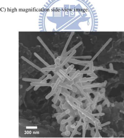
magnification surface image (inset, EDS of an area in (A)), (B) high magnification image, and (C) high magnification side-view image. ...27
Figure 2.3 A cluster of urchin-like Ag NWs formed initially on a SPC electrode at 2 h.
...27
Figure 2.4 XRD pattern of Ag NWs on a SPC electrode. ...28
Figure 2.5 (A) TEM image of urchin-like Ag NWs. SAED patterns from (B) the
white-dashed and (C) the yellow-dashed circles in (A)………29
Figure 2.6 Effect of lengths of growth time. SEM images of urchin-like Ag NWs
grown for (A) 1 h, (B) 3 h, and (C) 6 h...29
Figure 2.7 Proposed mechanism of urchin-like Ag nanowire...30
Figure 2.8 SEM images of Ag NWs on ITO substrates with different kinds seeding
laeyer. On Au seeding layer (A) Low magnification surface image (inset, EDS of an area in (A)), (B) high magnification surface image. On Pt seeding layer (C) Low magnification surface image (inset, EDS of an area in (C)), (D) high magnification surface image. (E) TEM image of Ag NWs in (C) (inset, [001] zone SAED of the Ag NW) (F) HRTEM image of the red marked circle region in (E). ...32
Chapter 3
Figure 3.1 SEM studies of urchin-like Ag NWs on a SPC electrode (A) Low
magnification surface image (inset, high magnification of a single cluster of urchin-like Ag NWs) (B) EDS of an area in (A). SEM images of urchin-like Ag NWs grown for (C) 1 h, (D) 3 h, and (E) 6 h. ...38
Figure 3.2 UV-visible absorption spectrum of urchin-like Ag NWs...39
Figure 3.3 SERS (Excitation: 532 nm, power: 5 mW, data collection: 5 s) of R6G (10 µL, in ethanol) on the urchin-like Ag NWs. The R6G concentrations are 10-13 M (red), 10-14 M(cyan), 10-15 M (blue), 10-16 M (green), and 10-17 M (black)...40
Figure 3.4 Raman spectra of R6G (1 µM, 10 µL, in ethanol) on urchin-like silver NWs with different growth time periods. (Excitation: 532 nm, power: 0.05 mW, data collection: 1 s)...41
Figure 3.5 Images of randomly selected areas (60 µm x 60 µm) of urchin-like Ag NWs on a SPC electrode. Series (A) - (F), optical images and corresponding Raman mappings of the R6G signals at 614 cm-1, 776 cm-1, 1366 cm-1, 1509 cm-1, and 1650 cm-1. ...43
Figure 3.6 Raman spectra of the R6G signals in Figure 3.5. (A) (B) (C) spectra are
the signals in Figure 3.5(B) from left to right. (D), (E), (F) spectra are the signals come from Figure3.5 (C), (E), (F), respectively………..45
Figure 3.7 Time-resolved surface-enhanced Raman spectra of R6G (10 µL, 1 fM) molecule recorded at 3-s intervals. Over 160 spectra were recorded before the signals disappeared. Ten spectra were selected to highlight sudden spectral changes. The table displayed five main Raman signals in these spectra. The Raman signals abruptly changed in both frequency and intensity. The laser excitation wavelength was 532 nm and the power was about 5 mW...46
Figure 3.8 SERS of R6G on urchin-like Ag NWs (10 fM, red) and on a glass slide
(0.1 M, black). (Excitation: 532 nm, power: 5 mW, data collection: 5 s)...47
Figure 3.9 Raman spectrum of R6G (1 µM, 10 µL, in ethanol) on urchin-like silver NWs (Detected by MiniRam™ II Raman Spectrometer System, excitation: 785 nm, power: 5 mW, data collection: 5 s). ...48
Chapter 4
Figure 4.1 Two-electrode electrodeposition system. ...56
Figure 4.2 (A) SEM image of Ag urchin-like NWs on an SPC electrode (inset:
enlarged view of a single cluster of urchin-like Ag NWs). (B) EDS of an area in part A. (C) SEM image of Ag microparticles on an SPC electrode. (D) EDS of an area in part C...57
Figure 4.3 CVs of different H2O2 concentrations in deaerated PBS (pH 7.4, 0.01 M)
using an Ag NW electrode as the working electrode. The H2O2 concentrations are 0
mM (dot), 2 mM (dash), 4 mM (dash dot), and 6 mM (solid). The scan rate is 50 mV/s. ...58
Figure 4.4 Comparison of CV scans before (solid) and after (dashed) addition of
H2O2 (6 mM) in deaerated PBS (pH 7.4, 0.01 M). The working electrodes are (A) Ag
NWs, (B) Ag microparticles and (C) screen printed carbon electrodes. The scan rate is 50 mV/s...59
deaerated PBS (pH 7.4, 0.01 M) on (a) Ag micro particles electrode (black) at -0.4 V and (b) Ag NW electrode (red) at -0.28 V. Inset shows the lowest concentration to be detected at 10 µM. ...60
Figure 4.6 (A) Calibration curves of amperometric tests in Figure 5. (B) Calibration
curves (current density normalized by mass) of amperometric tests in Figure 5. The working electrodes are Ag NWs (black triangle) and Ag microparticles (black square). The error bars indicated the standard deviation of three successive measurements....61
Figure 4.7 Stripping voltammetry of Ag NWs in a 0.1 M NaClO4 solution at a scan
rate ν = 20 mV/s...62
Figure 4.8 Interference analysis by amperometry at -0.28 V. The injection sequences
are UA (saturated), AA (2 mM), glucose (6 mM), NaCl (0.15 M), NaHCO3 (27 mM),
followed by H2O2 (1 mM) additions in deaerated PBS (pH 7.4, 0.01 M). ...64
Chapter 5
Figure 5.1 Successive UV-vis absorption spectra of the reduction of 4-NP by NaBH4
in the presence of Ag NWs (t=22 min). The right inset shows the logarithm of the absorbance at 400 nm vs reduction time. The left inset shows the photographs of the reduction of 4-NP by NaBH4 in the absence (a) and presence (b) of Ag NWs. ...70
Figure 5.2 Optical Density at 600 nm in tubes with different samples. (A) SPC
electrode (B) Ag microparticles/SPC electrode (C) Ag NWs/SPC electrode...71
Appendix
Silver Nanowires: Preparation Properties and Sensing Applications
Student: Wei-Han Hsiao Advisor: Dr. Hsin-Tien Chiu Dr. Chi-Young Lee
Ph. D program
Department of Applied Chemistry National Chiao Tung University
Abstract
In this thesis, we demonstrate a simple low-cost galvanic reduction with surfactant-assisted method to grow urchin-like Ag nanowires (NWs) on electrodes.
First, urchin-like Ag NWs on screen-printed carbon (SPC) electrodes were prepared via glavanic reductions of AgNO3(aq) solutions in the presence of
cetyltrimethylammonium chloride (CTAC) by Cu foil. The diameters of the nanowires are about 80-120 nm, and their lengths are up to 10 µm. The Ag NW is single crystalline and tends to grow along the [110] direction. Moreover, we can use electrochemical deposition to synthesize Ag NW on Au or Pt seeding layers on Indium Tin Oxide (ITO) substrates with similar reaction condition.
The second subject is surface plamon resonance (SPR) property of urchin-like Ag NWs. The absorption peak at ca. 380 nm was attributed to the plasmon response from the transverse mode of the NWs while the broad band extended from 500 nm was assigned to the longitudinal modes of the NWs with different aspect ratios. Furthermore, we used Rhodamine 6G as the probe molecule, and the the excitation wavelength of 532 nm was applied for the surface enhanced Raman scattering (SERS)
experiments. The detection limit of Rhodamine 6G on the urchin-like Ag NWs can be as low as 10-16 M while the analytical enhancement factor is about 1013. Raman mapping images confirm that a single R6G molecule on the substrate can be detected.
The final subject is hydrogen peroxide sensing application. Cyclic voltammetric experiments using the Ag NWs as the working electrode showed electrocatalytic H2O2
reduction. For H2O2 sensing, the electrode exhibited a high sensitivity of 4705 µA
mM-1 mg-1 cm-2 from 50 µM to 10.35 mM and a measurable detection limit of 10 µM in amperometric detection. This is the first report on Ag NWs for non-enzymatic H2O2 sensing.
奈米銀線之製備
奈米銀線之製備
奈米銀線之製備
奈米銀線之製備、
、
、
、性質與感測應用
性質與感測應用
性質與感測應用
性質與感測應用
研究生: 蕭暐翰 指導教授: 裘性天 博士 李紫原 博士 國立交通大學應用化學系博士班
摘要
摘要
摘要
摘要
在本論文中,我們以賈凡尼還原法配合界面活性劑(烷基三甲基氯化銨)輔助 成長法,成功地將海膽狀奈米銀線成長於電極上。 首先,我們利用銅與硝酸銀的賈凡尼自發性氧化還原反應,在含有十六烷基 三甲基氯化銨與硝酸的水溶液中成長海膽狀奈米銀線於市售網版印刷碳電極 上,其直徑約為 80-120 nm,藉由不同的反應時間,長度可達 10 µm 左右。經由 結構分析顯示奈米銀線為單晶且成長方向為[110]。除此之外,我們也利用類似 的反應溶液,在鍍有金或鉑的氧化銦錫(ITO)導電玻璃上,以電化學沉積法也能 得到奈米銀線。 第二部分我們利用海膽狀奈米銀線,觀察其表面電漿共振特性。研究發現, 奈米銀線在紫外光區有表面電漿共振吸收特性,其主要吸收位置在 380 nm 與 500 nm 附近。我們更進一步的深入討論其在表面增強拉曼散射之應用,結果顯示當 我們以 532 nm 的雷射光作為激發光源,並以染料分子( Rhodamine 6G)作為偵測 分 子 , 可 以 得 到 最 佳 的 偵 測 極 限 為 10-16 M , 其 分 析 增 強 因 子 (AnalyticalEnhancement Factor)為 1013。利用表面增強拉曼光譜影像分析(SERS mapping
images),證明其有單分子偵測(single molecule detection)能力。
最後我們利用海膽狀奈米銀線作為電極,進行過氧化氫電化學感測實驗。循 環伏安法實驗展示海膽狀奈米銀線具有增強電催化過氧化氫還原的能力,在過氧
化氫安培法感測中,此電極展現高靈敏度(4705 µA mM-1 mg-1 cm-2),其偵測範圍
為 0.05 mM-10.35 mM,偵測極限可達 10 µM。這也是第一個利用奈米銀線作為
Acknowledgement
時光匆匆,沒想到我也有這一天。在交大念了十一年多的書,總算要離開, 感覺很不真實,也非常的開心。打從大三專題生起,就接受了裘性天老師的指導, 雖然我的個性並不細心,但隨著專題生,碩士班,到現在博士班可以畢業,全是 在裘老師叮嚀下,讓我在科學研究領域上,能有些微的成果與貢獻,甚至在人生 的道路上,也得到更多的經驗與指導。而在研究所期間,李紫原老師多元的想法 與建議,也讓我在思考研究上有更多的心得與收穫,更感謝老師們能參與我的終 生大事,讓我感到異常光榮。 感謝各位口試委員給予我論文的指導,黃暄益老師與李積琛老師在金屬材料 成長與光譜上的建議,以及廖奕翰老師在拉曼光譜數據上的指導,讓學生的論文 更加詳細清楚,也解決了許多內容上的缺失。 在研究的生活中,實驗室的夥伴是不可或缺的,上從大我七屆的學長,下至 小我七屆學弟妹,擁有你們這群生活上的夥伴,讓研究生的生活除了研究,也增 添了許多快樂的回憶,也因為這些 chiulab 的夥伴,使得大家在實驗不順遂時, 除了老師之外,你們大家提供了各式各樣的幫助,包括研究上與精神上,這都是 在我博士生涯中不可或缺的。 最後要感謝我的家人,爸媽一直都很擔心我是否能畢業,卻也不增添我的壓 力,岳父岳母更力挺我能順利的渡過這個人生的轉捩點。我的老婆,真的是讓妳 辛苦了,有妳的支持與諒解,我才能在最後這一年無後顧之憂的全力為我的論文 奮戰,也感謝有妳,我才能順利擁有一個獨一無二的兒子,也因為有妳們這些家 人,我才真正體會到什麼是娶某前生子後的好運氣,這一切的一切,都要感謝你 們! 最後的最後,我要跟大家說句經典名言:我要走了!Chapter 1
Introduction
1.1 Introduction
As we know, silver is widely used in our daily life such as jewelry, currency, mirrors and optics.1 In medical usage, silver compounds have been used to prevent infection in World War I before the advent of antibiotics.2 There are a lot of silver applications such as dentistry, photonics, photography, catalysis, electronics nowadays.3-5 In addition, bulk silver exhibits the highest electrical and thermal conductivities among all metals. Therefore, the exploration of silver applications is an important topic in future science.
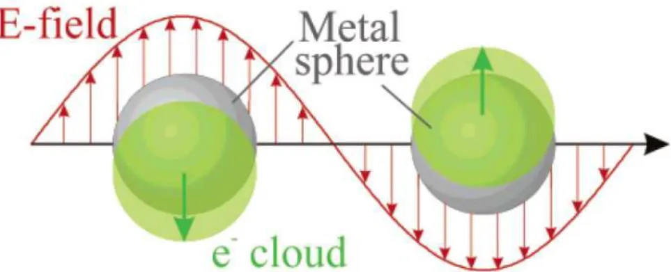
One-dimensional (1D) nanostructures (nanowire (NW), nanorod (NR), and nanotube (NT)) have been the focus of many recent studies due to their potential application in both interconnects and functional units of fabricating electronic, photonic, and sensing devices, which also provide an ideal model system to experimentally investigate physical phenomena, such as quantized conductance and size effects.6-19 Consequently, the synthesis and characterization of NWs have recently attracted attention from a great deal of researchers.20-23 Based on the unusual chemical and physical properties of 1D nanomaterials associated with the size and shape,24 lots of researchers have demonstrated that single one or arrays of 1D nanomaterials used as a building block in electronic, photonic, and sensing devices, which could attain miniaturization and enhance the performance. Among them, noble metal nanomaterials displays surface plasmon resonance (SPR),25 surface-enhanced Raman scattering (SERS),26 and electrochemical catalytic properties, which become a popular
Figure 1.1 Schematic of plasmon oscillation for a sphere, showing the displacement
of the conduction electron charge cloud relative to the nuclei.28
research subject. Until now, there have been few reports of 1D noble metal nanomaterials which are direct grown on hard template and their potential applications.
In this dissertation, 1D noble metal nanomaterials (urchin-like Ag NWs) were fabricated by surfactant assisted electrochemical methods. The intrinsic properties of urchin-like Ag NWs such as SERS performance and electrochemical catalysis would be investigated.
1.2 Properties and Applications of Silver Nanomaterials 1.2.1 Surface Plasmon Resonance (SPR) Absorption
It is interesting to see metal nanoparticles (NPs) with different colors. For examples, Au colloidal NPs are brilliant red and Ag NPs are typically yellow. In the middle 1800s, Michael Faraday synthesized colloidal solutions of gold exhibiting colors range from rube red to amethyst.27 The various colors resulted from the surface plasmon band (SPB), which is a phenomenon observed in transmission, due to the presence of NPs, in solution or in the solid phase. When a small spherical metallic NP is irradiated by light, the oscillating electric field causes the conduction electrons to oscillate coherently (show in Figure 1.1).28 When the electron cloud is displaced
relative to the nuclei, a restoring force arises from Coulomb attraction between electrons and nuclei that results in oscillation of the electron cloud relative to the nuclear framework.
In 1908, Mie presented a solution to Maxwell’s equations29-31 that describes the extinction spectra (extinction = scattering + absorption) of spherical particles of arbitrary size. Until now, several numerical techniques based on finite elements have been demonstrated the limitation in calculations of particles with arbitrary shape and muitcomposition.32, Among them, the discrete dipole approximation (DDA) has been proven to be an effective technique for estimating the optical properties of metal NPs.33 The extinction spectra of metal NPs under various conditions were mostly simulated by the DDA calculation and compared with the experimental results.34 The influence of particle shapes on SPR wavelengths was also investigated.
The particle size, shape, and intrinsic dielectric constant are an important factor to the SPR wavelength. A lot of researches concerning the size effect of spherical NPs have been reported.35 Besides, the geometry of metal particles also have strong influences on the SPR peaks such as nanoprisms and nanocubes. The phenomenon is usually occurred in Ag nanomaterials with different shapes. For example, Schatz and co-workers have illustrated that the increase of the side length of Ag nanoprisms could lead their SPR peak to red shift by several hundred nanometers.36 In the case of Ag NRs or NWs, there are two SPR peaks which would change with the aspect ratio of the Ag 1D nanomaterials.25 This is due to the absorption of visible light both along the length of the nanorod (the longitudinal plasmon band) and along the width of the nanorod (the transverse plasmon band). The larger the aspect ratio, the more red-shifted the longitudinal plasmon band, as theory predicts37 and experiment confirms.38-42
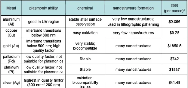
Table 1.1 Comparison of the Suitability of Different Metals for Plasmonic
Applications.50
a: metal cost (2011/9/11) can be found at the Web site: http://www.kitco.cn/hk/metal-
market/precious-metals/precious-metals-market.htm
interesting, and it enables the particles to be applied in biological sensing and drug delivery.43,44 As a result, silver is probably the most important material in plasmonics. It offers many advantages over Au, Cu, and Al which are other metals known to support surface plasmons (SPs) in the visible (vis) and near-infrared regions (NIR).45,46 In terms of plasmonics, it is important to choose a metal that can support a strong SP at the desired resonance wavelength.47,48 The SP strength is directly proportional to the quality factor (Q).46 Ag has the largest quality factor across most of the spectrum from 300 to 1200 nm. In contrast, Al is only suitable for applications in the ultraviolet (UV) region. For Au and Cu, their SPR excitation wavelengths are longer than 500 and 600 nm, respectively.49 Furthermore, the difficulty of fabricating nanostructures, and their cost, will also determine the usefulness of a metal for SPR applications, especially for large-scale applications. As shown in Table 1.1, silver is relatively cheap among the metals that support plasmons and easy to fabricate.50 To
sum up, Ag compared with the other metals is unique for its excellent qualities in terms of SPR ability, available nanostructures, and material cost.
1.2.2 Surface-Enhanced Raman Scattering (SERS)
In 1928, Indian scientist Sir C. V. Raman observed the Raman effect by means of sunlight and won the Nobel Prize in Physics in 1930. Raman spectroscopy displays the change in wavelength that is attributed to the excitation (or relaxation) of vibrational modes of a molecule when a photon undergoes Raman scattering. Since vibrational information is specific to the chemical bonds and symmetry of molecules. Therefore, each molecule can be identified and shows a unique fingerprint in a Raman spectrum. In accordance with the Raman selection rule, the molecular polarizabilty changes as the molecular vibrations displace the constituent atoms from their equilibrium positions. The amount of the polarizability change will determine the Raman scattering intensity. Hence, aromatic molecules usually exhibit more intense Raman scattering than aliphatic molecules.
In general, Raman spectroscopy has lots of advantages for microscopic analysis. For examples, specimens do not need to be fixed or sectioned; Raman spectra can be collected from a very small volume (< 1 µm in diameter); water does not generally interfere with Raman spectral analysis. However, there are some limitations for the applicability of Raman scattering such as the intrinsic small intensity of the Raman signal, the sensitivity limit of available detectors, and the intensity of the excitation source.
In 1974, SERS from pyridine adsorbed on electrochemically roughened silver was produced by Martin Fleischman and coworkers.51 After that, Jeanmaire and Van Duyne demonstrated that the magnitude of the Raman scattering signal can be greatly enhanced when the scattering is placed on or near a roughened noble metal substrate.26 This is called electromagnetic effect, which is one of the SERS
mechanisms. Strong electromagnetic fields are generated when the localized surface plasmon resonance (LSPR) of nanoscale roughness features on silver or gold substrates is excited by visible light. When the Raman scatterer is subjected to these intensified electromagnetic fields, the magnitude of induced dipole increases, and accordingly, the intensity of the inelastic scattering increases. This is the main factor in SERS. The other factor is called chemical effect,52 which is contributing enhancement only on the order of an order or two of magnitude.53 The chemical enhancement involves changes to the adsorbate electronic states due to chemisorption of the analyte which results in charge transfer between metal and adsorbate. Until now, the exact mechanism of the enhancement effect of SERS is still a matter of debate in the literature. These two factors are generally approved.
In order to know the performance of the SERS, definitions of SERS enhanced factor (EF) have been investigated. The most widely used definition for the average SERS EF equation is shown below:54
EF=(ISERS/NSurf)/(IRS/NVol) (1.1)
where NVol is the average number of molecules in the scattering volume (V) for the
Raman (non SERS) measurement, and NSurf is the average number of adsorbed
molecules in the scattering volume for the SERS experiments. The rigorous definition:
Nsurf=µMµSAMAeff (1.2)
Nvol=CRSV=CRSHeffAeff (1.3)
where µM is the surface density of the individual nanostructures with respect to the
main plane forming the substrate, µS is the surface density of molecules on the metal,
AM is the metallic surface area in each nanostructure, CRS is the concentration used for
the non-SERS spectra, Heff is the effective height of the scattering volume, and Aeff is
volume but for 2D).
As a result of the complicated definition, all the factors are not easy to ensured or estimated in every experimental condition.
The definitions described above have attempted to emphasize the intrinsic characteristics of the substrate and are not always straightforward to relate to experimental results. For many applications, however, one is mostly concerned with the simple question of how much more signal can be expected from SERS as compared to normal Raman under given experimental conditions. To address this question, another definition of SERS EF which is fairly intuitive and particularly relevant for analytical chemistry applications is introduced. It is called the analytical enhancement factor (AEF) which is presented by the equation:54
AEF=(ISERS/CSERS)/(IRS/CRS) (1.4)
Here, IRS represents the Raman intensity of an analyte with a concentration CRS on a
non-SERS substrate. ISERS is obtained from a SERS-active substrate with an analyte
concentration CSERS. In the experiments, all the other parameters, including laser
wavelength, laser power, microscope magnification, and spectrometer are identical. The AEF in fact ignores the fact that SERS is a type of surface spectroscopy, which means that only the adsorbed molecules contribute to the signal, and that the effect is distance dependent.
Nowadays, SERS can be exploited for sensitive and selective molecular identification. In 1997, Shuming Nie has successfully proved that single rhodamine 6G (R6G) molecule could be probed with Ag NPs by SERS.55 In recent years, other single molecule detections have been reported, too.56-65 Therefore, SERS has been used extensively as a signal information in biological and chemical sensing such as protein,66-68 DNA69,70, and environmental pollutants.71-74 A miniaturized, inexpensive, and portable SERS instrument makes the technique practical for trace analysis in
clinics, the field, and urban settings.75
1.2.3 Catalytic Properties
Silver is a common heterogeneous catalysis in the chemical industry. It can synthesize various chemicals and reduce production cost. For example, the selective oxidation of ethylene to ethylene epoxide (also known as ethylene oxide) is an important industrial catalytic reaction. Silver is considered almost the unique effective catalyst for ethylene epoxidation76 and α-Al2O3 is the preferred support. Moreover,
Styrene (C6H5CH=CH2) and epoxides are industrially important bulk chemicals,
which are largely used for synthesis of several perfumes, epoxy resins, plasticizers and drugs. Epoxidation of styrene to styrene oxide (SO) by molecular oxygen was also studied using the silver catalysts.77
Reduction of 4-aminophenol (4-AP) is also an important subject and the conventional methods for hydrogenation of 4-NP involve iron/acid as a reducing agent.78 The reason is that manufacturing of many analgesic and antipyretic drugs, such as paracetamol, phenacetin, and so on, needs 4-AP as a potent intermediate. It is also used enormously as a photographic developer, corrosion inhibitor, anticorrosion- lubricant, and hair-dyeing agent.79,80 As we know, reduction of aromatic nitro compounds is inert to sodium borohydride (NaBH4) reaction if it is used alone.
Catalytic reduction of aromatic nitro compounds by coinage metal nanoparticles has been reported.81 Here, Ag nanomaterials have also shown their worth for catalytic reduction of 4-AP by using NaBH4 as an alternative effective and eco-friendly
method.82,83
1.2.4 Electrochemical Property and Sensing
Electrochemical reactions taking place at the interface between flat electrodes and electrolyte solutions are often impeded by diffusion process. In order to overcome this problem, fabrication of nanostructured electrodes with the high roughness (ratio of
real surface area to geometric area) are developed. These electrodes display high electrochemical active surface areas and accelerate the electrochemical reactions. Therefore, there are many NP-modified electrodes fabricated such as silver, gold, and platinum NP electrodes which are used as a excellent electron transfer mediator.84-86
The size dependent electrocatalytic behaviors of nanomaterials of silver, platinum and gold has been demonstrated previously.87-91 Moreover, electrocatalytic behaviors on various morphology of nanomaterial electrodes have been investigated in recent years.92-101 In general it is accepted that catalytic activity is related to the surface energy of exposed crystal faces. The structure of low-index planes are regarded as surface defects play a significant role in electrocatalysis.102-104
Silver is a highly active electrocatalyst in alkaline solutions for the oxidation of small organic molecules, due to the formation of reactive adsorbed OH species that influence the kinetics of the reaction. 93,102,105-109 Also, it has been demonstrated that nanosized Ag can act as an effective sensing material for the detection of pesticides110 and toxic substances such as lead111 as well as important species such as hydrogen peroxide,108,112 nitrates,113-115 and hydrazine.116
1.3 Various Synthetic Strategies of 1D Metal Nanomaterials 1.3.1 Direct Hard Template Method
In general, channels in porous membranes provide a typical template for use in the synthesis of 1D nanostructure (Fig 1.2).24 This method was demonstrated by Martin and several others. 117-119 Until now, anodic aluminum oxide (AAO) is the most widely used hard template.120 Figure 1.2 shows that NWs and NTs can be formed by full and part filled channels with desire materials, respectively.121-123 For example, Wu et al. and Choi et al. have employed AAO-assisted electrochemical deposition to fabricate Ag NWs with adjustable diameter and high aspect ratio.124,125 Other hard templates such as step-edge surface,126 DNA molecules127,128 have also reported.
Figure 1.2 Scheme of NWs and NTs formation by filling and partial filling the pores
within a porous membrane with the desired material or precursor to this material.24
Figure 1.3 (A) self-assembled reverse micelle and (B) capping reagent mechanism of
surfactants.129
1.3.2 Micelle and Reversed Micelle Methods
This method is also called soft template method which is the early procedure for fabricating NPs. Surfactants have both hydrophilic and hydrophobic tails and self-assemble into reversed micelles with various shapes in aqueous solution, as show in Figure 1.3A.129 Nanocrystals are formed by reducing metal ions in this microreactor and stably dispersive in solution.130,131 Hong et al. used the pores of self-assembled calix[4]hydroquinone nanotubes as a soft template to synthesize ultrathin single crystalline Ag NWs arrays by electro/photochemical redox reaction in
complete filling
incomplete filling
an ambient aqueous phase.132
1.3.3 Seed-Mediated Growth
Murphy and coworkers have developed seed-mediated growth to fabricate and contol 1D metal nanomaterials.25 The procedure begins with the synthesis of metallic nanospheres by chemical reduction of a metal salt with a strong reducing agent such as NaBH4. Citrate is present as a capping agent to prevent particle growth. The gold
or silver spheres thus generated are 3±5 nm in diameter and serve as seeds on which to grow more anisotropic nanostructures. When adding seeds into the reaction solution contained metal salts, weak reducing agent, and surfactants, the reaction would be activated and metal atoms could deposit selectively on the seeds to form anisotropic growth. NRs and NWs with an uniform diameter and controllable aspect ratio were fabricated in the presence of 4 nm Ag seeds, AgNO3/ ascorbic acid growth
solution and cetyltrimethylammonium bromide (CTAB).41 For Au NRs, the synthesis is similar, too.42 Figure 1.3B displays that bilayer structures of surfactants (CTAB) self-assemble adsorbed selectively on specific crystal facets and confine their growth.129 The relative growth rate between capped and uncapped sites results in the formation of NRs or NWs. CTAB, called capping reagent, play an important role for controlling anisotropic crystal growth.
1.3.4 Polyol Process
Xia and coworkers recently demonstrated a poloyol method that generated Ag NWs by reducing AgNO3 with ethylene glycol in the presence of poly(vinyl pyrrolidone)
(PVP).133,134 Ethylene glyol served as both solvent and reducing agent. The key to formation of wire-like nanostructures is the introduction of exotic seeds (Pt NPs) to the reaction mixture and the using of PVP as a polymeric capping reagent which adsorbed on Ag nanocrystal surfaces by O atoms confirmed by X-ray photoelectron spectra (XPS).135
Figure 1.4 Scheme of growth mechanism of Cu Nanobelt and Ag Belt-like
materials.136
1.3.5 Galvanic Displacement Reduction
Most of methods described above are homogeneous solution reaction. In 2007, we evolved heterogeneous galvanic displacement reduction to fabricate Cu and Ag nanobelts (NBs).136 Sacrificial metals oxidized itself and reduced the other metal ions at the interface of metal and solution as shown in Figure 1.4. We used cetyltrimethyl- ammonium chloride (CTAC) as a capping reagent to successfully grow and immobilize the diverse nanostructures on electrodes at the same time. Moreover, we also fabricate Cu NBs137 and Au NWs138,139 on electrodes in similar reaction condition by electrochemical deposition.
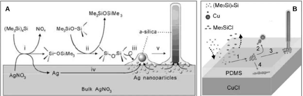
1.3.6 Vapor-Solid Reaction Growth (VSRG)
Our group develop a route of vapor solid reaction growth to synthesize cable-like Cu and Ag NWs.140,141 CuCl encapsulated in poly(dimethylsiloxane) (PDMS) and tetrakis(trimethylsilyl) silane (TTMS, Si(SiMe3)4) as a reducing agent were sealed in a
Figure 1.5 Scheme of cable-like NWs growth mechanism (A) Ag/SiO2 NWs (B)
Cu/PDMS NWs.140,141
the reaction, cable-like Cu/PDMS NWs were produced. On the other hand, AgNO3
and (Me3Si)4Si were reacted in a sealed tube under low pressure at 400 K in 10 min
and held at the temperature for 2 h and cable-like Ag/SiO2 NWs were generated.
Figure 1.5 display the mechanisms of growth cable-like Cu and Ag NWs.140,141
1.3.7 Arc Discharge Method
An electric arc is an electrical breakdown of a gas which produces an ongoing plasma discharge, resulting from a current flowing through normally nonconductive media such as air. Arc discharge process is the first and now widespread method of carbon NTs production. Wang et al. reported that high density and high purify Ag-core/C-shell nanocables could be synthesized via a hydrogen arc discharged method.142 The cathode was a solid randomly oriented graphite (ROG) rod, and the anode is a cup-like ROG rod filled with carbon black and Ag powder. The diameter of the Ag-core is dependent on the percentage of Ag present in the anode.
1.3.8 Solid-Liquid Phase Arc Discharge (SLPAD) Method
Zhou and coworkers report a novel method for preparation of silver nanowires via a so-called solid liquid phase arc discharge method (SLPAD).143 High-purity silver filaments were used as two electrodes and NaNO3 was used as electrolyte. It formed
the instantaneous circulation between the two electrodes and arc discharge sparks
while a certain voltage was used. It is well-known that the arc discharge released great exothermic heat, leading to the occurrence of the continuous dissolution of silver electrodes in a form of silver clusters. These clusters entered into NaNO3 solution in a
possible shape of the tadpole-like or column-like morphology and the cooling water will restrain the contraction of these shaped clusters and prevented them from becoming spherically shaped. These factors may be favorable for the formation of the Ag NWs.
1.4 Aim of This Thesis
In recent years, there are great deals of reports about synthesizing Ag nanomaterials due to their interesting morphology related chemical and physical properties. Among them, many researchers are interested in sensing applications of Ag nanomaterials such as SERS and electrocatalysis. Until now, most of Ag nanomaterials synthetic methods require multiple steps, strict conditions, and cost much. Especially, there are few reports regarding direct growth of 1D Ag nanomaterials on electrodes for sensing applications in the past years.
In this thesis, we demonstrate a simple low-cost surfactant-assisted galvanic reduction process to direct grow urchin-like Ag NWs on carbon screen printed electrodes. According to the intrinsic properties of Ag, SERS and electrocatalysis sensing applications of urchin-like Ag NWs are investigated. The detail studies would be presented in the following chapters.
1.5 References
1. Wilson, Ray N. Reflecting Telescope Optics: Basic design theory and its
historical development. Springer. 2004 p. 422.
2. Medical uses of silver can be found at the Web site: http://en.wikipedia.org/wiki/ Medical_uses_of_silver#cite_note-31
3. Jin, R.; Cao, Y.; Mirkin, C. A.; Kelly, K. L.; Schatz, G. C.; Zheng, J. G. Science
2001, 294, 1901.
4. Hoelderich, W. F. Catal. Today 2000, 62, 115.
5. Gould, I. R.; Lenhard, J. R.; Muenter, A. A.; Godleski, S. A.; Farid, S. J. Am.
Chem. Soc. 2000, 122, 11934.
6. Favier, F.; Walter, E. C.; Zach, M. P.; Benter, T.; Penner, R. M. Science 2001,
293, 2227.
7. Cui, Y.; Wei, Q.; Park, H.; Lieber, C. M. Science 2001, 293, 1289.
8. Gudiksen, M. S.; Lauhon, L. J.; Wang, J.; Smith, D. C.; Lieber, C. M. Nature
2002, 415, 617.
9. Hu, J.; Odom, T. W.; Lieber, C. M. Acc. Chem. Res. 1999, 32, 435. 10. Sun, L.; Searson, P. C.; Chien, C. L. J. Chem. Phys. 2001, 79, 4429. 11. Peng, X. Adv. Mater. 2003, 15, 459.
12. Iijima, S. Nature 1991, 354, 56.
13. Ebbesen, T. W.; Ajayan, P. M. Nature 1992, 358, 220. 14. Morales, A. M.; Lieber, C. M. Science 1998, 279, 208. 15. Han, W.; Fan, S.; Li, Q.; Hu, Y. Science 1997, 277, 1287.
16. Dai, H.; Wong, E. W.; Lu, Y. Z.; Fan, S.; Lieber, C. M. Nature 1995, 375, 769. 17. Saito, S. Science 1997, 278, 77.
18. Bockrath, M.; Cobden, D. H.; McEuen, P. L.; Chopra, N. G.; Zettl, A.; Thess, A.; Smalley, R. E. Science 1997, 275, 1922.
19. Suenaga, K.; Colliex, C.; Demoncy, N.; Loiseau, A.; Pascard, H.; Willaime, F.,
Science 1997, 278, 653.
20. Lu, Q.; Gao, F.; Komarneni, S. Langmuir 2005, 21, 6002.
21. Dai, Y.; Zhang, Y.; Bai, Y. Q.; Wang, Z. L. Chem. Phys. Lett. 2003, 375, 96. 22. Qian, W.; Wei, F.; Liu, T.; Wang, Z. W. Solid State Commun. 2003, 126, 365. 23. Gundiah, G.; Deepak, F. L.; Govindaraj, A.; Rao, C. N. R. Chem. Phys. Lett.
2003, 381, 579.
24. Xia, Y.; Yang, P.; Sun, Y.; Wu, Y.; Mayers, B.; Gates, B.; Yin, Y.; Kim, F.; Yan, H.
Adv. Mater. 2003, 15, 353.
25. Murphy, C. J.; Jana, N. R. Adv. Mater. 2002, 14, 80.
26. Jeanmaire, D. L.; Van Duyne, R. P. J. Electroanal. Chem. 1977, 84, 1. 27. Faraday, M. Philos. Trans. 1857, 147, 145.
28. Kelly, K. L.; Coronado, E.; Zhao, L. L.; Schatz, G. C. J. Phys. Chem. B 2002,
107, 668.
29. Mie, G. Ann. Phys. 1908, 25, 377.
30. Kerker, M. The Scattering of Light and Other Electromagnetic Radiation; Academic: New York, 1969.
31. Bohren, C. F.; Huffman, D. R. Absorption and Scattering of Light by Small
Particles; Wiley Interscience: New York, 1983.
32. Waterman, P. C. Phys. Rev. D 1971, 3, 825.
33. Yang, W. H.; Schatz, G. C.; Duyne, R. P. V. J. Chem. Phys. 1995, 103, 869. 34. Duval Malinsky, M.; Kelly, K. L.; Schatz, G. C.; Van Duyne, R. P. J. Phys. Chem.
B 2001, 105, 2343.
35. Messinger, B. J.; von Raben, K. U.; Chang, R. K.; Barber, P. W. Phys. Rev. B
1981, 24, 649.
Nature 2003, 425, 487.
37. El-Sayed, M. A. Acc. Chem. Res. 2001, 34, 257.
38. Foss, C. A.; Hornyak, G. L.; Stockert, J. A.; Martin, C. R. J. Phys. Chem. 1994,
98, 2963.
39. Yu; Chang, S.-S.; Lee, C.-L.; Wang, C. R. C. J. Phys. Chem. B 1997, 101, 6661. 40. Link, S.; Mohamed, M. B.; El-Sayed, M. A. J. Phys. Chem. B 1999, 103, 3073. 41. Jana, N. R.; Gearheart, L.; Murphy, C. J. Chem. Commun. 2001, 617.
42. Jana, N. R.; Gearheart, L.; Murphy, C. J. J. Phys. Chem. B 2001, 105, 4065. 43. West, J. L.; Halas, N. J. Annu. Rev. Biomed. Eng. 2003, 5, 285.
44. Moores, A.; Goettmann, F. New J. Chem. 2006, 30, 1121. 45. Wiley, B.; Sun, Y.; Xia, Y. Acc. Chem. Res. 2007, 40, 1067.
46. Ru, E. L.; Etchegoin, P. Principles of Surface Enhanced Raman Spectroscopy; Elsevier: Oxford, U.K., 2009.
47. Lal, S.; Link, S.; Halas, N. J. Nat. Photonics 2007, 1, 641. 48. Link, S.; El-Sayed, M. A. J. Phys. Chem. B 1999, 103, 8410.
49. Wang, H.; Tam, F.; Grady, N. K.; Halas, N. J. J. Phys. Chem. B 2005, 109, 18218.
50. Rycenga, M.; Cobley, C. M.; Zeng, J.; Li, W.; Moran, C. H.; Zhang, Q.; Qin, D.; Xia, Y. Chem. Rev. 2011, 111, 3669.
51. Fleischmann, M.; Hendra, P. J.; McQuillan, A. J. Chem. Phys. Lett. 1974, 26, 163.
52. Albrecht, M. G.; Creighton, J. A. J. Am. Chem. Soc. 1977, 99, 5215.
53. Kambhampati, P.; Child, C. M.; Foster, M. C.; Campion, A. J. Chem. Phys. 1998,
108, 5013.
54. Le Ru, E. C.; Blackie, E.; Meyer, M.; Etchegoin, P. G. J. Phys. Chem. C 2007,
55. Nie, S.; Emory, S. R. Science 1997, 275, 1102.
56. Kneipp, K.; Wang, Y.; Kneipp, H.; Perelman, L. T.; Itzkan, I.; Dasari, R. R.; Feld, M. S. Phys. Rev. Lett. 1997, 78, 1667.
57. Michaels, A. M.; Jiang; Brus, L. J. Phys. Chem. B 2000, 104, 11965. 58. Bosnick, K. A.; Jiang, J.; Brus, L. E. J. Phys. Chem. B 2002, 106, 8096. 59. Futamata, M.; Maruyama, Y.; Ishikawa, M. Vib. Spectrosc 2004, 35, 121. 60. Futamata, M.; Maruyama, Y.; Ishikawa, M. J. Phys. Chem. B 2004, 108, 13119. 61. Wilson, R.; Bowden, S. A.; Parnell, J.; Cooper, J. M. Anal. Chem. 2010, 82,
2119.
62. Sawai, Y.; Takimoto, B.; Nabika, H.; Ajito, K.; Murakoshi, K. J. Am. Chem. Soc.
2007, 129, 1658.
63. Rao, S.; Raj, S.; Balint, S.; Fons, C. B.; Campoy, S.; Llagostera, M.; Petrov, D.
Appl. Phys. Lett. 2010, 96, 213701.
64. Wang, Y.; Lee, K.; Irudayaraj, J. J. Phys. Chem. C 2010, 114, 16122.
65. Lim, D.-K.; Jeon, K.-S.; Kim, H. M.; Nam, J.-M.; Suh, Y. D. Nat. Mater. 2010, 9, 60.
66. Wang, Y.; Wei, H.; Li, B.; Ren, W.; Guo, S.; Dong, S.; Wang, E. Chem. Commun.
2007, 5220.
67. Ni, J.; Lipert, R. J.; Dawson, G. B.; Porter, M. D. Anal. Chem. 1999, 71, 4903. 68. Hu, J.; Zheng, P.-C.; Jiang, J.-H.; Shen, G.-L.; Yu, R.-Q.; Liu, G.-K. Anal. Chem.
2008, 81, 87.
69. Hu, J.; Zheng, P.-C.; Jiang, J.-H.; Shen, G.-L.; Yu, R.-Q.; Liu, G.-K. Analyst
2010, 135, 1084.
70. Braun, G.; Lee, S. J.; Dante, M.; Nguyen, T.-Q.; Moskovits, M.; Reich, N. J. Am.
Chem. Soc. 2007, 129, 6378.
Edit. 2008, 47, 6456.
72. De Jesús, M. A.; Giesfeldt, K. S.; Sepaniak, M. J. J. Raman Spectrosc. 2004, 35, 895.
73. Halvorson, R. A.; Vikesland, P. J. Environ. Sci. Technol. 2010, 44, 7749. 74. Li, X.; Chen, G.; Yang, L.; Jin, Z.; Liu, J. Adv. Funct. Mater. 2010, 20, 2815. 75. Young, M. A.; Stuart, D. A.; Lyandres, O.; Glucksberg, M. R.; Van Duyne, R. P.
Can. J. Chem. 2004, 82, 1435.
76. Campbell, C. T. J. Phys. Chem. 1985, 89, 5789.
77. Chimentao, R.; Medina, F.; Sueiras, J.; Fierro, J.; Cesteros, Y.; Salagre, P. J.
Mater. Sci. 2007, 42, 3307.
78. Crossley, M. L. Ind. Eng. Chem. 1922, 14, 802. 79. John F, C. Dyes Pigment. 1999, 41, 127.
80. Rode, C. V.; Vaidya, M. J.; Chaudhari, R. V. Org. Process Res. Dev. 1999, 3, 465.
81. Pradhan, N.; Pal, A.; Pal, T. Langmuir 2001, 17, 1800.
82. Saha, S.; Pal, A.; Kundu, S.; Basu, S.; Pal, T. Langmuir 2009, 26, 2885. 83. Rashid, M. H.; Mandal, T. K. J. Phys. Chem. C 2007, 111, 16750.
84. Lee, C.-L.; Chiou, H.-P.; Syu, C.-M.; Wu, C.-C. Electrochem. Commun. 2010,
12, 1609.
85. Jena, B. K.; Raj, C. R. Chem. Eur. J. 2006, 12, 2702.
86. Hrapovic, S.; Liu, Y.; Male, K. B.; Luong, J. H. T. Anal. Chem. 2003, 76, 1083. 87. Chen, W.; Chen, S. Angew. Chem. Int. Ed. 2009, 48, 4386.
88. Park, S.; Xie, Y.; Weaver, M. J. Langmuir 2002, 18, 5792.
89. Rhee, C. K.; Kim, B.-J.; Ham, C.; Kim, Y.-J.; Song, K.; Kwon, K. Langmuir
2009, 25, 7140.
Markovic, N. M. J. Phys. Chem. B 2005, 109, 14433.
91. Campbell, F. W.; Belding, S. R.; Baron, R.; Xiao, L.; Compton, R. G. J. Phys.
Chem. C 2009, 113, 9053.
92. Bansal, V.; Li, V.; O'Mullane, A. P.; Bhargava, S. K. CrystEngComm 2010, 12, 4280.
93. Geng, J.; Bi, Y.; Lu, G. Electrochem. Commun. 2009, 11, 1255. 94. Yuan, J. H.; Wang, K.; Xia, X. H. Adv. Funct. Mater. 2005, 15, 803.
95. Zhuang, Z.; Su, X.; Yuan, H.; Sun, Q.; Xiao, D.; Choi, M. M. F. Analyst 2008,
133, 126.
96. Park, S.; Chung, T. D.; Kim, H. C. Anal. Chem. 2003, 75, 3046.
97. Song, Y.-Y.; Zhang, D.; Gao, W.; Xia, X.-H. Chem. Eur. J. 2005, 11, 2177. 98. Subhramannia, M.; Ramaiyan, K.; Pillai, V. K. Langmuir 2008, 24, 3576.
99. Chen, Y.; Schuhmann, W.; Hassel, A. W. Electrochem. Commun. 2009, 11, 2036. 100. Vidal-Iglesias, F. J.; Solla-Gullón, J.; Rodrı́guez, P.; Herrero, E.; Montiel, V.;
Feliu, J. M.; Aldaz, A. Electrochem. Commun. 2004, 6, 1080. 101. Zeng, J.; Zhang, Q.; Chen, J.; Xia, Y. Nano Lett. 2009, 10, 30. 102. Burke, L. D.; Ryan, T. G. J. Appl. Electrochem. 1990, 20, 1053.
103. Nowicka, A. M.; Hasse, U.; Sievers, G.; Donten, M.; Stojek, Z.; Fletcher, S.; Scholz, F. Angew. Chem. Int. Ed. 2010, 49, 3006.
104. Koper, M. T. M. Faraday Discuss. 2009, 140, 11.
105. Demarconnay, L.; Coutanceau, C.; Léger, J. M. Electrochim. Acta 2004, 49, 4513.
106. Chatenet, M.; Micoud, F.; Roche, I.; Chainet, E. Electrochim. Acta 2006, 51, 5459.
107. Guo, D. J.; Li, H. L. Carbon 2005, 43, 1259.
Mater. Lett. 2009, 63, 969.
109. Blizanac, B. B.; Ross, P. N.; Marković, N. M. J. Phys. Chem. B 2006, 110, 4735. 110. Marenco, A. J.; Pedersen, D. B.; Wang, S.; Petryk, M. W. P.; Kraatz, H.-B.
Analyst 2009, 134, 2021.
111. Bonfil, Y.; Brand, M.; Kirowa-Eisner, E. Electroanalysis 2003, 15, 1369.
112. Welch, C. M.; Banks, C. E.; Simm, A. O.; Compton, R. G. Anal. Bioanal. Chem.
2005, 382, 12.
113. Krista, J.; Kopanica, M.; Novotný, L. Electroanalysis 2000, 12, 199. 114. Kim, D.; Goldberg, I. B.; Judy, J. W. Analyst 2007, 132, 350.
115. Fajerwerg, K.; Ynam, V.; Chaudret, B.; Garçon, V.; Thouron, D.; Comtat, M.
Electrochem. Commun. 2010, 12, 1439.
116. Yang, G.-W.; Gao, G.-Y.; Wang, C.; Xu, C.-L.; Li, H.-L. Carbon 2008, 46, 747. 117. Martin, C. R. Science 1994, 266, 1961.
118. Martin, C. R. Acc. Chem. Res. 1995, 28, 61.
119. C. Hulteen, J.; Martin, C. R. J. Mater. Chem. 1997, 7, 1075. 120. Jessensky, O.; Müller, F.; Gösele, U. Appl. Phys. A 1998, 72, 1173.
121. Gao, T.; Meng, G.; Zhang, J.; Sun, S.; Zhang, L. Appl. Phys. A 2002, 74, 403. 122. Tao, G.; et al. J. Phys.: Condens. Matter 2002, 14, 355.
123. Li, N.; Li, X.; Yin, X.; Wang, W.; Qiu, S. Solid State Commun. 2004, 132, 841. 124. Wu, Y.; Livneh, T.; Zhang, Y. X.; Cheng, G.; Wang, J.; Tang, J.; Moskovits, M.;
Stucky, G. D. Nano Lett. 2004, 4, 2337.
125. Choi, J.; Sauer, G.; Nielsch, K.; Wehrspohn, R. B.; Gösele, U. Chem. Mater.
2003, 15, 776.
126. Walter, E. C.; Murray, B. J.; Favier, F.; Kaltenpoth, G.; Grunze, M.; Penner, R. M. J. Phys. Chem. B 2002, 106, 11407.
128. Monson, C. F.; Woolley, A. T. Nano Lett. 2003, 3, 359.
129. 黃亭凱, 裘性天, 李紫原,電化學法成長金屬奈米材料,國立交通大學應
用化學研究所博士論文,民國九十八年
130. Filankembo, A.; Pileni, M. P. J. Phys. Chem. B 2000, 104, 5865.
131. Pileni, M. P.; Ninham, B. W.; Gulik-Krzywicki, T.; Tanori, J.; Lisiecki, I.; Filankembo, A. Adv. Mater. 1999, 11, 1358.
132. Hong, B. H.; Bae, S. C.; Lee, C.-W.; Jeong, S.; Kim, K. S. Science 2001, 294, 348.
133. Sun, Y.; Gates, B.; Mayers, B.; Xia, Y. Nano Lett. 2002, 2, 165.
134. Sun, Y.; Yin, Y.; Mayers, B. T.; Herricks, T.; Xia, Y. Chem. Mater. 2002, 14, 4736.
135. Huang, H. H.; Ni, X. P.; Loy, G. L.; Chew, C. H.; Tan, K. L.; Loh, F. C.; Deng, J. F.; Xu, G. Q. Langmuir 1996, 12, 909.
136. Huang, T.-K.; Cheng, T.-H.; Yen, M.-Y.; Hsiao, W.-H.; Wang, L.-S.; Chen, F.-R.; Kai, J.-J.; Lee, C.-Y.; Chiu, H.-T. Langmuir 2007, 23, 5722.
137. Huang, T. K.; Lin, K. W.; Tung, S. P.; Cheng, T. M.; Chang, I. C.; Hsieh, Y. Z.; Lee, C. Y.; Chiu, H. T. J. Electroanal. Chem. 2009, 636, 123.
138. Huang, T.-K.; Chen, Y.-C.; Ko, H.-C.; Huang, H.-W.; Wang, C.-H.; Lin, H.-K.; Chen, F.-R.; Kai, J.-J.; Lee, C.-Y.; Chiu, H.-T. Langmuir 2008, 24, 5647.
139. Yang, Y.-C.; Huang, T.-K.; Chen, Y.-L.; Mevellec, J.-Y.; Lefrant, S.; Lee, C.-Y.; Chiu, H.-T. J. Phys. Chem. C 2011, 115, 1932.
140. Yen, M. Y.; Chiu, C. W.; Hsia, C. H.; Chen, F. R.; Kai, J. J.; Lee, C. Y.; Chiu, H. T. Adv. Mater. 2003, 15, 235.
141. Hsia, C.-H.; Yen, M.-Y.; Lin, C.-C.; Chiu, H.-T.; Lee, C.-Y. J. Am. Chem. Soc.
2003, 125, 9940.
H. Appl. Phys. A 2007, 87, 1.
143. Zhou, Y.; Yu, S. H.; Cui, X. P.; Wang, C. Y.; Chen, Z. Y. Chem. Mater. 1999, 11, 545.
Chapter 2
Growth of Urchin-like Silver Nanowires by Surfactant-Assisted
Galvanic Reductions
2.1 Introduction
In recent years, a lot of researchers are interested in one-dimensional (1D) nanomaterials of noble metal due to their special electrical, optical, and chemical properties, which are different or superior to the bulk ones.1-3 Among all the noble metal, silver is highly attractive because of the highest electrical and thermal conductivities. Furthermore, silver has the potential of using as active components in catalysis, photography, electronics, photonics, information storage, optoelectronics, biological labeling, imaging, and sensing.4-7 Therefore, there are a great deal of researches to synthesize silver nanowires (Ag NWs). Until now, various kinds of techniques have been developed such as arc-discharge,8 template assisted by anoidic aluminum oxide (AAO)9 or polymer membranes,10 polyol process,11,12 seed-mediated growths,13,14 etc. Here, we report a surfactant assisted synthesis of urchin-like Ag NWs on screen-printed carbon (SPC) electrodes via glavanic reductions of AgNO3(aq)
solutions in the presence of cetyltrimethylammonium chloride (CTAC) by Cu foil. We expect the urchin-like Ag NW may find applications in surface-enhanced Raman scattering (SERS) spectroscopy,15,16 electrochemical sensor for nitrite17,18 or hydrogen peroxide,19,20 and antibacterial.21,22
2.2 Experimental
2.2.1 Preparation of Growth Substrates
A Cu foil (5 x 5 mm2) was pre-cleaned with HCl(aq) (Tedia, 0.1 N) for 3 min and
rinsed by deionized water. Then, the foil was adhered to a commercial SPC electrode (Zensor R&D SE100, 0.196 cm2) with conductive silver (Ted Pella). The whole assembly was baked at 353 K in an oven for 30 min.
2.2.2 Preparation of Urchin-like Ag NWs
AgNO3 (Mallinckrodt, 0.064 g, 0.375 mmol) was added to a stirring aqueous
solution of CTAC (Taiwan Surfactant, 5.4 x 10⁻³ M, 50 mL) and HNO3 (Showa, 5 x
10-3 M) in a glass beaker. Immediately, the mixture turned white and opaque. After the colloidal suspension was stirred for 15 min, it was allowed to stand for 15 min more. Then, the assembled growth substrate was immersed into the mixture at 303 K for 6 h. After the Cu foil was detached from the electrode, the substrate was rinsed by deionized water. To avoid oxidation, the as-prepared Ag NWs electrodes were stored in a N2 filled glove box to prevent surface oxidation.
2.2.3 Characterization
The scanning electron microscopic (SEM) and energy dispersive spectroscopic (EDS) data were taken from a Hitachi S-4000 (25 keV) and a JEOL JSM-7401F (15 keV). Transmission electron microscope (TEM) and selected area electron diffraction (SAED) images were captured by a JEOL JEM-2010 at 200 kV. The X-ray diffraction (XRD) patterns were acquired by using a Bruker AXS D8 Advance.
2.3 Results and Discussion
2.3.1 SEM and EDS Characterization
After AgNO3(aq) was added to a stirring solution containing CTAC(aq) and
HNO3(aq), the mixture turned white and opaque immediately. This indicated the
Figure 2.1 Optical images of the commercial SPC electrode (A) before and (B) after
the Ag NW growth.
of Cu foil attached to its contact was immersed. The exposed electrode surface turned gray gradually (Figure 2.1). To avoid oxidation, the as-prepared Ag NWs electrodes were stored in a N2 filled glove box to prevent surface oxidation. In Figure 2.2A, a
SEM image shows that the electrode surface is covered by a lot of urchin-like NWs. Based on the EDS measurement displayed in Figure 2.2A (inset), we conclude that the NWs are composed of Ag only. The C signal is assigned to the SPC substrate. From the high magnification image displayed in Figure 2.2B, some branching of the NWs can be observed. The diameters of the NWs are estimated to be about 100 nm while the lengths are found to be in the range 3 – 10 µm. With different growth conditions, the diameters can vary from 80 to 120 nm while the lengths can differ from 1 to 10
µm. An individual cluster of NWs formed initially at 2 h (Figure 2.3) show that many NWs protruded from a surface on the substrate to form the urchin-like morphology. The side-view image is shown in Figure 2.2C. We can notice that whole urchin-like Ag NWs arise from the electrode surface. The image displays that in each urchin-like structure, the NWs radiate from an apparent common nucleus. Other growth conditions of different Ag samples are shown in appendix.
(A)
(B)
(A)
Figure 2.2 SEM studies of urchin-like Ag NWs on a SPC electrode. (A) Low
magnification surface image (inset, EDS of an area in (A)), (B) high magnification image, and (C) high magnification side-view image.
Figure 2.3 A cluster of urchin-like Ag NWs formed initially on a SPC electrode at 2
h.
(C)
(B)
(A)
(C)
(C)
(B)
(B)
(A)
(A)
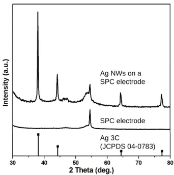
Figure 2.4 XRD pattern of Ag NWs on a SPC electrode.
2.3.2 XRD Analysis
The XRD patterns are shown in Figure 2.4. The peaks at 2θ=38.1°, 44.3°, 64.5°, 77.4° are assigned to Ag (111), (200), (220), and (311) reflections, respectively (JCPDS file 04-0783).23 The broad band around 54° comes from the SPC electrode. From the patterns, the lattice parameter a was estimated to be 0.409 nm, consistent with the value reported for Ag.23
2.3.3 TEM Characterization
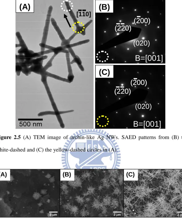
TEM studies of a group of urchin-like NWs are shown in Figure 2.5. The image in Figure 2.5Areveals an overall morphology closely related to the ones presented in Figure 2.2C and Figure 2.3. Extension of the NWs from an apparent initial growth point and branching of some NWs are observed. The SAED patterns of the tip and the root of a NW, which branches from another NW stem, are shown in Figure 2.5B and 2.5C, respectively. Interestingly, they display the same set of dot patterns revealing their single crystalline nature. They both correspond to the [001] crystallographic zone axis of an fcc structure with the lattice parameter a calculated to be 0.41 nm.23
SPC electrode Ag 3C (JCPDS 04-0783) Ag NWs on a SPC electrode In te n s it y ( a .u .)
Figure 2.5 (A) TEM image of urchin-like Ag NWs. SAED patterns from (B) the
white-dashed and (C) the yellow-dashed circles in (A).
Figure 2.6 Effect of lengths of growth time. SEM images of urchin-like Ag NWs
grown for (A) 1 h, (B) 3 h, and (C) 6 h.
The NW growth direction is determined to be along the [-1-10] direction. The data suggest that the overall branched Ag NW structure is a single crystal.
2.3.4 Reaction Time Influence
SEM images of urchin-like Ag NWs grown from different lengths of time were shown in Figure 2.6. At 1 h, there were few urchin-like NWs with lengths less than 1
(A)
(020)
(220)
(200)
B=[001]
(B)
B=[001]
(020)
(220)
(200)
(C)
[110]
(A)
(020)
(220)
(200)
B=[001]
(B)
(020)
(220)
(220)
(200)
(200)
B=[001]
(B)
B=[001]
(020)
(220)
(200)
(C)
B=[001]
(020)
(220)
(220)
(200)
(200)
(C)
[110]
(A)
(B)
(C)
(A)
(A)
(B)
(B)
(C)
(C)
Figure 2.7 Proposed mechanism of urchin-like Ag nanowire.
µm on the SPC electrode (Figure 2.6A). At 3 h, more urchin-like clusters with longer NWs were observed, as shown in Figure 2.6B. When the growth was extended to 6 h, more coverage of longer NWs on the electrode surface was found in Figure 2.6C.
2.3.5 Proposed Growth Mechanism
We suggest that our previously proposed growth pathways for one-dimensional Cu, Ag, and Au nanostructures are applicable for the urchin-like Ag NWs too.13,24-26 The preparation of Ag NW is dependent on the presence of CTAC and HNO3. All the
growth process is presented in Figure 2.7. At the beginning, there are 7.5 mM Ag+(aq)
ions in this reaction solution. Some Ag+(aq) ions (2.1 mM) would reduce by Cu(s) to
form Ag(s) clusters through the galvanic reduction, 2Ag+(aq) + Cu(s) → 2Ag(s) + Cu2+(aq)
E° = 0.46 V.27 The clusters enlarged as more Ag(s) reduced to become urchin nucleus on the electrode. At the same time, the other Ag+(aq) ions (5.4 mM) combined with
e
-Carbon electrode
Ag Ag AgAg Cu C Cu C Cu C 7.5 mM AgNO3(aq) Ag+(aq) e -Ag+(aq) e -hυυυυ AgCl(s) AgCl(s) (CTAC) CH3(CH2)15N(CH3)3+Cl -Cl -(CTAC) CH3(CH2)15N(CH3)3+Cl -Cl -Cu(s) Cu2+ (aq)e
-Cu(s) Cu2+ (aq)e
-Ag(s) 5.4 mM CTAC(aq) 5 mM HNO3(aq)Cl-(aq) anions (5.4 mM) from CTAC molecules to form AgCl(s) colloids which covered
by a shell of CTAC molecules. Since the reaction 2AgCl(s) + Cu(s) → 2Ag(s) + Cu2+(aq)
+ 2Cl-(aq) E° = -0.12 V27 is not thermodynamically favored, the source of Ag cannot
obtained via this route. The growth cannot just proceed via the reaction 2Ag+(aq) + Cu(s)
→ 2Ag(s) + Cu2+(aq) without CTAC either because this reaction alone did not produce
the urchin-like NWs structure. As the literature reports, it is known that AgCl(s) can be
reduced to Ag(s) by light.28 The Ag(s) clusters reduced by light could be seeds
randomly adsorbed on the urchin nucleus and initiated the growth of Ag NWs assisted by CTAC as the surface capping reagent, which may selectively adsorbed on low-index facets to form a bilayer interface structure.29,30 The presence of NO3-(aq) ions
in the growth solution is another determinant for controlling the crystal shape in the system. The function of the ions may oxidize Ag(s) into Ag+(aq) ions. During the crystal
growth, the less stable facets might be oxidized by NO3-(aq) easily, leaving the more
stable facets exposed for further developments. As a result, all these factors function cooperatively in the reaction to direct the crystals to grow into urchin-like Ag NWs.
2.3.6 Extensive Application on Electrochemical Deposition
In our reaction, reduction of Ag+(aq) ions were contributed by galvanic reductions.
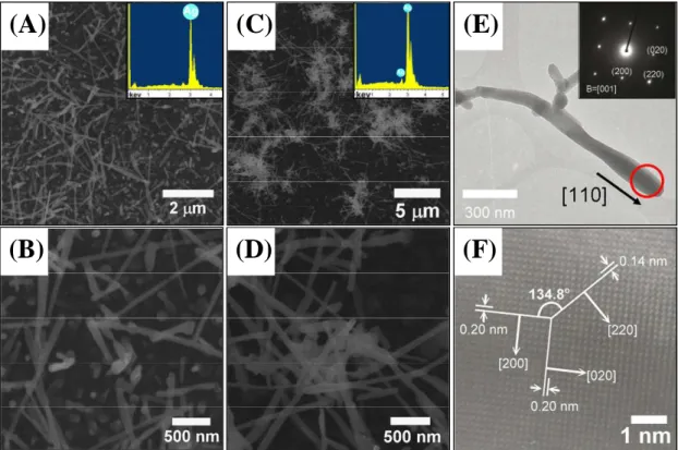
However, we discovered that Ag NWs could be grown direct on Au or Pt seeding layers on Indium Tin Oxide (ITO) substrate via a simple two-electrode electrochemical deposition method in the same reaction solution at 293 K. The results are shown in Figure 2.8. Figure 2.8A to 2.8D display that there are some Ag NWs on the ITO substrates. The diameters are about 60 nm, which are smaller than the ones react by galvanic reductions. The lengths are found to be in the range 1 – 5 µm. Based on the EDS measurement displayed in Figure 2.8A (inset) and 2.8C (inset), we
Figure 2.8 SEM images of Ag NWs on ITO substrates with different kinds seeding
laeyer. On Au seeding layer (A) Low magnification surface image (inset, EDS of an area in (A)), (B) high magnification surface image. On Pt seeding layer (C) Low magnification surface image (inset, EDS of an area in (C)), (D) high magnification surface image. (E) TEM image of Ag NWs in (C) (inset, [001] zone SAED of the Ag NW) (F) HRTEM image of the red marked circle region in (E).
conclude that the NWs are composed of Ag only. TEM characterizations are displayed in Figure 2.8E and 2.8F. The SAED pattern in Figure 2.8E (inset) shows a spot pattern, which can be indexed to be [001] zone axis of Ag reveals that the Ag NW is single crystalline. From the pattern, the growth direction of Ag NW is determined to be along [110] direction, which is identical to the one reacted by galvanic reduction. Figure 2.8F presents an HRTEM image from the red marked circle region in Figure 2.8E. The dihedral angle between [220] and [200] is 134.8°, which is close to the theoretical value of an fcc structure. The [220] and [200] d-spacing are measured to be
(A)
(B)
(C)
(D)
(E)
(F)
0.14 nm and 0.20 nm, respectively. Both the value are close to the previous report of Ag, 0.144 nm and 0.204 nm.23
2.4 Conclusion
In summary, we have developed a simple low-cost surfactant-assisted galvanic reduction process to grow urchin-like Ag NWs on SPC electrodes. Both CTAC and HNO3 molecules are essential ingredients to shape the urchin-like Ag NW. Moreover,
we can use electrochemical deposition to synthesize Ag NW on Au or Pt seeding layers on ITO substrates with similar reaction condition.