characteristics of PGI circuits can be approximately predicted and several handy equations, which are useful for pencil-and-paper design, can also be found for planning the desired circuit to achieve good enough performance with an acceptable accuracy tolerance in the steady state. In addition, an optimized design method for PGI circuits with resistive loads is developed in terms of the total number of gain stages in the design and the ratio between pump capacitors. For 1.5 V supply voltage operation, re-liability and accuracy are demonstrated by comparisons between SPICE simulations of the PGI circuit and the results from the equivalent model. The model also has been validated by means of measurements taken from a test chip and typically shows relative open-loop output voltage errors lower than 8%. Finally, although the derivation of the model was based on a PGI circuit, it is shown that the design strategy can also be applied to other charge pump designs that have no voltage drop between the inner stages and the output stage.
Index Terms—Charge pump, dc–dc converter, equivalent model,
high-voltage generator, voltage multiplier.
I. INTRODUCTION
I
N modern mixed-mode circuit designs, low-voltage and small-size dc–dc converters have been extensively required. Charge pump circuits (CPCs) can provide the solutions neces-sary to meet these demands to convert an input voltage upward to a higher one with either a positive or a reverse polarity. Since CPCs use capacitors as energy storage devices instead of magnetic components, the converter has no electromagnetic interference (EMI) problems. For low-power designs, the ca-pacitors required by CPCs can be small enough to be fabricated in integrated circuits.CPCs have been widely used in nonvolatile memories for many years, such as EEPROM and Flash memories [1]–[4]. More and more applications of CPCs can be found in power in-tegrated circuits (ICs), low-supply-voltage switched-capacitor systems, continuous time filters [5], adaptive voltage-scaling power management [6], and so on. Most of the conventional CPCs are based on the circuit proposed by Dickson [7] as shown in Fig. 1(a). It uses diode-connected transistors as charge-transfer devices. Neglecting the body effect and using the steady-state analysis from the simple model of the Dickson
Manuscript received May 14, 20007; revised August 19, 2007. Published June 20, 2008. This work was supported in part by the National Science Council of Taiwan, R.O.C., under Project NSC 96-2221-E-009-239-MY3.
The authors are with the Electrical and Control Engineering Department, Na-tional Chiao Tung University, Hsingchu 300, Taiwan, R.O.C. (e-mail: chhu. [email protected]; [email protected]; [email protected]).
Digital Object Identifier 10.1109/TPEL.2008.926950
be expressed as
(1) where is the pumping clock amplitude, is the clock fre-quency, is the output current, and is the voltage drop across each MOS diode. In (1), the first term is the common expression for the voltage increase occurring at each pumping node contributed by the clock source, clk or , through the as-sociated capacitor . The second term is the voltage drop due to . In each stage, the necessary condition for the boost func-tion of the CPC is that must be larger than zero. With the condition that and are constants, the final output voltage in an -stage CPC with a resistive load can be obtained as
(2) where is the input voltage. From (1) and (2), an extremely simple equivalent circuit for the Dickson charge pump is shown in Fig. 1(b) and the output voltage can be derived as
(3) where
and . In (3), and are the
equivalent open-circuit output voltage and the equivalent output series resistance, respectively.
However, is not a constant because is enlarged by the body effect, which increases as more pump stages are used. The body effect increases the threshold voltage, , and results in the degradation of . Thus, the pumping efficiency of the succeeding stage will be less than that of the forestages. When in the last stage reduces to zero, will start to saturate even if more cascaded pump stages are added. Another voltage drop problem exists at the output stage, because the most se-rious body effect occurs on due to a large build up of . The loss of pumping gain also results in an increased power loss. This low efficiency restricts the application of the Dickson charge pump structure to low-supply voltage dc–dc converters. In recent years, much effort has been made in the analysis and optimization of the Dickson structure [10], [11], and many ap-proaches for improving the pumping efficiency have focused on solving the threshold voltage augmentation problem [12]–[16]. Some of them offer a high pumping gain in the inner stage and a very low voltage drop at the output stage. Thus, the voltage gain of these circuits can be maintained to keep the output voltage proportional to the number of pump stages. In this article, in
Fig. 1. (a) Dickson charge pump circuit. (b) Equivalent model of the Dickson charge pump.
order to support a convenient and rapid design scheme, a thor-ough analysis and a complete model of the pumping gain in-crease (PGI) circuit [16], which is a type of improved CPC, has been presented. In Section II, a general model based on PGI cir-cuits is described. Analyses based on the charge balance and average conceptions are presented. By using this simple analyt-ical model, characterization of PGI circuits can be performed in a pencil-and-paper manner and the output behavior can be approximately predicted. An optimization design method for minimizing the die area of an -stage PGI circuit in terms of the total number of pump stages and the pump capacitors ratio is also presented. This design strategy can also be applied to other improved CPC designs that have no voltage drop be-tween inner stages and the output stage. In Section III, simu-lation results are presented to verify this equivalent model for designing PGI circuits. In Section IV, experimental results mea-sured from a test chip that was fabricated with a TSMC 0.35- m mixed-mode technology demonstrate the validity of the pro-posed model. Conclusions are given in Section V.
II. EQUIVALENTMODEL FOR THEVOLTAGEMULTIPLIER
PGI circuits provide a method of using NMOS and PMOS charge transfer switches (CTSs) to eliminate the voltage drop, , across each pump stage and allow the output voltage to increase linearly as the cascade number of the pump stage increases. The schematic diagrams of one-stage PGI circuits, which approximately double their supply voltage, are shown in Fig. 2. It is notable that in PGI-3, there is no output saturation limitation, no matter how many pump stages are used. Ignoring non-ideal characteristics such as switching losses and parasitic capacitances, an analytically ideal model can be constructed based on the identity of an -stage PGI circuit.
Fig. 2. Voltage doubling PGI circuits. (a) PGI-3 circuit. (b) PGI-1 circuit [16].
Fig. 3. Conceptual diagram of anN-stage PGI circuit.
A. Behavioral Model of Intermediate Stages
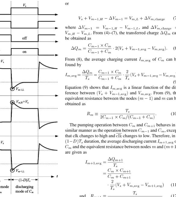
From the characteristics of an -stage PGI circuit, the equiv-alent circuit can be simplified as shown in Fig. 3, where clk and are two anti-phase clocks with the same amplitude, , is the pump capacitor of the th pump stage, is a time-variant voltage across , is the voltage at node connecting to the positive branch of , and is the th equivalent ideal transfer switch between and . Each stage has two op-erating modes, the charging mode opop-erating with duration and the discharging mode with duration, where is the duty ratio and is the switching period. The corresponding waveforms of , , and are shown in Fig. 4. In order to find a general model, the charge balance and the average of are used to calculate the transfer charge and the average current between pump capacitors. In Fig. 4, in-creases from the lowest level, , to the highest level, , in the charging mode of and decreases back to in the
Fig. 4. Clock signal, states of switches, and the steady-state waveforms of V ,V , andV .
discharging mode. Let denote the arithmetic average of and and be given as
(4) Similar notations are also applied to all the voltages across the pump capacitors. From Fig. 4, in time , is raised by , and part of the charge stored in will transfer to . Thus, will increase from to , and will decrease from to . By using charge conser-vation, can be expressed as
(5) If is sufficiently large to complete the charge transfer in time, the following expressions can be obtained:
(6)
From (8), the average charging current of can be found by
(9) Equation (9) shows that is a linear function of the
dif-ference between and . From (9), the
equivalent resistance between the nodes and can be obtained as
(10) The pumping operation between and behaves in a similar manner as the operation between and , except that clk changes to high and changes to low. Therefore, in a duration, the average discharging current of and the equivalent resistance between nodes and are given as
(11)
and (12)
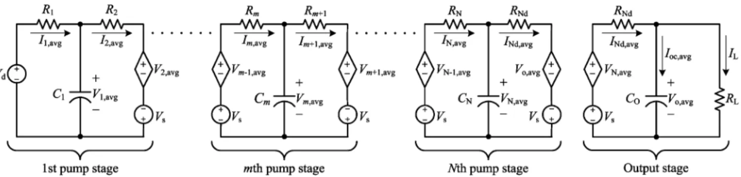
Since (9)–(12) shows a simple and regular modular structure, the equivalent model of each intermediate stage of PGI circuits can be deduced as the th pump stage model shown in Fig. 5.
B. Behavioral Model of the Input Stage
In the first stage, since is connected to a voltage source , the average voltage of can be given as
(13) In the charging mode of , increases from the lowest level to . From (13), the transferred charge can be ex-pressed by and . The corresponding average charging current of and the resultant equivalent resistor are given as
(14) and
Fig. 5. Equivalent model for anN-stage PGI circuit.
Fig. 6. Steady-state waveforms ofV andV .
The operation of in its discharging mode is the same as that of the inner pump capacitor. Thus, employing (11)–(15), the equivalent model of the first pump stage in the PGI circuit can be depicted as shown in Fig. 5.
C. Behavioral Model of the Output Stage
The load can be generally represented by a resistor, , con-nected in parallel to the output capacitor, . Thus, the behavior of the charge transmitted to during each cycle period must be included in the model operation. According to Fig. 3, the waveforms of and the output voltage, , are given in Fig. 6. In the charging period of , is turned on and the charge is quickly delivered from to in a very short period, . This causes to increase from to . After , and discharge through as a parallel capaci-tance . At the end of the , both and will decrease from their high level to a voltage as follows:
(16)
where , and and are the
voltage drop values in the periods of and , as shown in Fig. 6. When the discharging period
of starts, is turned off and the consumed charge of is provided only by . By employing the average def-inition of as (6) in a cycle time, and can be derived as
(17a)
and (17b)
where and . From (17),
is smaller than because is produced from the discharge of and is produced only from the dis-charge of .
Employing (16), (17), and the charge conservation within , , and , the voltage variations , , , and can be found. Using these voltage variations to derive the charge transfer rate, the average discharging current of corresponding to , which is the charge delivered from to , can be simply obtained as
(18) Comparing (18) with (11), is different from all the av-erage discharging currents of the inner pump stages. Similarly to (18), the average charging current of can be de-rived as
(19) The equivalent circuit model provided by (18) and (19) can be simplified greatly if is equal to . This condition can be met by choosing and such that
By using (21)–(23), the equivalent model of the last pump stage and the output stage can be obtained as shown in Fig. 5. In the complete circuit model, all labeled voltages are averages and each dependent voltage source is controlled by its corresponding voltage across a capacitor. Based on this regular and simplified model, the behavior of a multistage PGI circuit with a resistive load can be easily controlled and designed.
D. Results Obtained From Equivalent Model
In Fig. 5, all capacitors can be considered open when the PGI circuit reaches the steady state. Although the model of each stage contains four voltage sources, for an -stage PGI circuit, the average output can be found and expressed simply by (24)
Replacing by an approximate value of , (24) can be rewritten as
(25)
where represents the total capacitance of all the pump capacitances connected in series. The result expressed by (25) shows that is determined by the ratio of to the
con-stant . Thus, if the time constant is
smaller than , can be effectively regulated by tuning the switching period . From (25) an alternative expression of
in terms of the load current can be obtained as (26) In (26), the highest ideal output voltage will occur with the condition of 0. As the load current increases, the output voltage will decrease at a rate of [17]. Moreover, if pump capacitors are all the same value, it can be seen that the derived result (26) would match Dickson’s result (3) with 0 and 0. This comparison proves that the proposed model deduced from PGI circuits is an ideal case of the Dickson structure. Consequently, even though the model and the derivation were based on PGI circuits, the same design strategy can be applied, as an ideal case, to any charge-pump design which is able to eliminate voltage drop between the inner stages and the output stage.
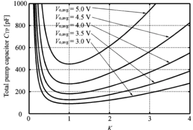
Considering chip size and therefore cost, decreasing the sum of pump capacitances will greatly decrease the die area.
Fig. 7. Total pump capacitancesC calculated from the three-stage model versus the value ofK under various desired V , whereV = V = 1.5 V, R = 100 k, and f = 1 MHz.
Assuming that the pump capacitances are designed proportion-ally as , where is a regulative constant, of an -stage PGI circuit can be obtained from (25) and ex-pressed as
(27) From (27), the minimum can be found by making 0. This derivation has a reasonable solution which is 1. Thus, the minimum value of each pump capacitance referred as is given by
(28) Fig. 7 shows the relation between and for various se-lected in the three-stage example. It can be seen that the minimum occurs at 1. In addition, by solving 0 for a fixed , the optimum number of stages associated with the minimum can be found. The solu-tion is given as
(29) The optimum value of must be an integer near the result of (29). Fig. 8 provides the information needed to find the value of for generating a specified with minimum . As an example, by using the results from Fig. 7 and Fig. 8, a PGI circuit with an output voltage of 4 V across a resistive load of 100 k can be designed for a minimum with 3 and
60 pF.
III. MODELVALIDATION
In order to validate the accuracy of the derived model, SPICE simulations are performed for both the equivalent three-stage PGI circuit shown in Fig. 3 and the corresponding model, where 1.5 V, 100 k , 1 mHz, and was deter-mined by employing the relation between and from (20).
Fig. 8. Total pump capacitancesC versus the stage numberN over various desiredV , whereV = V = 1.5 V, R = 100 k, and f = 1 MHz.
Fig. 9. Comparison between the simulated output waveforms of the equivalent three-stage PGI circuit and the corresponding model.
Fig. 9 shows the output simulation waveforms of the equivalent three-stage circuit and the model, respectively, where the simu-lation conditions are 60 pF ( 1, 2, 3), 200 pF, 40 A, and 0.57. Under these design conditions, the output ripple is limited to 0.2 V, and the mean of the undu-lated output voltage is 4 V, which is equal to of the model in steady state. A satisfactory agreement between the two simu-lations can be observed during the procedure of boosting. From additional simulation data with different values and various numbers of pump stages, the output values of the models al-ways follow the undulated output waveforms of the equivalent PGI circuits. Consequently, these simulation results show that the presented model can predict the output behavior of a multi-stage PGI circuit with a resistive load.
In common uses, the duty ratio of CPCs is usually set to 0.5. However with this configuration, (20) is ineffective in finding a suitable value of for equating to shown in Fig. 6. If , will be close to and the difference between and can be reduced. Oth-erwise, a slightly greater error will exist. Fig. 10(a) shows the difference error of and the mean of the undulated output voltage of the equivalent three-stage PGI circuit obtained from the SPICE simulation results when a square clock waveform 0.5 is employed. In addition, the corresponding value of is shown in Fig. 10(b). From Fig. 10, it can be seen that the larger the value of , the smaller the relative error and output
Fig. 10. (a) Relative errors between the model and the three-stage PGI circuit for different desiredV withV = V = 1.5 V, R = 100 k, f = 1 MHz, andD = 0.5. (b) Corresponding output ripple 1V .
ripple . If is larger than 200 pF, it appears that the error and are less than 0.4% and 0.2 V, respectively.
A practical embodiment of a three-stage PGI-3 circuit, which is built by the circuit shown in Fig. 2(a), was simulated in the MOS level by using parameters of a TSMC 0.35- m mixed-mode mixed-model and general clocks 0.5 . With the same sim-ulated conditions used in Fig. 9, except that the duty ratio 0.5, the transient simulation waveforms are shown in Fig. 11. From the simulation results, the final mean value of the practical circuit is about 3.95 V, and the error between this mean value and the final value of from the model is about 1.25%. Besides the influence of , this small error is most likely due to the fact that switching losses and parasitic capacitances of the practical circuit are taken into account in the SPICE simulation but not included in the model. In addition, the full practical circuit sim-ulation waveform lags slightly behind that of the model. This waveform lag is due to the fact that gate control voltages of the transfer switches generated by CTSs in the PGI circuit would not be pumped to the levels for turning on the switches com-pletely in the initial few cycles. In summary, the output behavior and the final of the model closely match the simulation results of the practical PGI circuit.
IV. MEASUREMENTRESULTS
In order to validate results of the analysis and design consid-erations, several PGI circuits with different numbers of stages were fabricated in a TSMC 0.35- m mixed-mode process. To increase the flexibility of measurements, pump capacitors were
Fig. 11. Comparison between the simulated output waveforms of the practical three-stage PGI circuit and the corresponding model.
Fig. 12. Measured output voltages of a two-stage PGI-3 circuit under different values ofC .
connected externally. A two-stage PGI circuit was tested under
1.5, 100 k , 330 pF, 1 MHz,
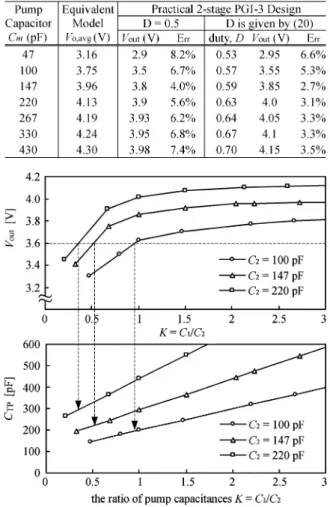
and . Three kinds of output voltage data are plotted in Fig. 12 for the comparison. Two are obtained from the measured output voltages for 0.5 and the value cal-culated from (20). The third is obtained from the simulation results of the presented model. The performance data and the corresponding errors are summarized in Table I. For this typ-ical example, the measured output voltages are close to of the model, e.g., for 100 pF, the mean of the measured output voltages are 3.5 and 3.55 V when 0.5 and 0.57 calculated from (20), respectively, and is 3.75 V when using the model simulation. It can be seen from Table I that the error voltages in this case are lower than 0.25 V, and all the rela-tive errors of the measurements are less than 8%. The measured output voltages are smaller than the model simulation output voltage , due to additional parasitic capacitors, parasitic resistors, and extra switching losses. In the case of above 150 pF, where is above 0.45, Fig. 12 also shows that the measured as obtained from (20) is more accurate than that measured as 0.5. However, even though the ratio of is increased, the relative errors in the case of 0.5 only increase slightly. This agrees with the theoretical re-sults depicted in Fig. 10.
Further experiments of the two-stage PGI circuit at 0.5 were also taken by changing the ratio of to . The mea-sured data are shown in Fig. 13. The curves of -to- and
Fig. 13. Measured output voltages of a two-stage PGI-3 circuit with a different ratio ofC and C .
-to- give information that 1 is the optimum selec-tion to generate a desired dc output voltage. For instance, when 3.6 V is considered, Fig. 13 shows that 1 gives the minimum . This observation is in accordance with the prediction of (28).
V. CONCLUSION
An analysis and modeling technique of on-chip charge pumps with a resistive load based on PGI circuits has been proposed. The equations of the model also have been deduced for design within an acceptable accuracy tolerance. By using the presented model and equations, the output behavior can be approximately predicted and the capacitances and the switching period can be determined while satisfying the requirement of a desired final output voltage with a ripple . Based on the analysis pre-sented, with a given resistive load and a desired output voltage across it, an optimal number of pump stages and equalized pump capacitors have been proved for the objective of minimum total pump capacitance, which represents minimum chip size. In ad-dition, the influence of the duty ratio on the output voltage and the accuracy of the model under general clocks 0.5 have been discussed. The simulation results of the presented model and the SPICE simulations of PGI circuits exhibit satisfactory
agreement on transient behavior and the final value of the output voltage. Analysis of the measurement results for an integrated two-stage PGI-3 circuit at light loading also has validated the model. A comparison of data shows that the relative errors are lower than 8%. Furthermore, since the structure of each pump stage model is simple and regular, it is easy to construct the com-plete model of a multistage PGI circuit.
REFERENCES
[1] A. Umezawa, S. Atsumi, M. Kuriyama, H. Banba, K. I. Imamiya, K. Naruke, S. Tamada, E. Obi, M. Oshikiri, T. Suzuki, and S. Tanaka, “A 5-v-only operation 0.6 um flash EEPROM with row decoder scheme in triple-well structure,” IEEE J. Solid-State Circuits, vol. 27, no. 11, pp. 1540–1545, Nov. 1992.
[2] T. Kawahara, T. Kobayashi, Y. Jyouno, S. Saeki, N. Miyamoto, T. Adachi, M. Kato, A. Sato, J. Yugami, H. Kume, and K. Kimura, “Bit-line clamped sensing multiplex and accurate high voltage generator for quarter-micron flash memories,” IEEE J. Solid-State Circuits, vol. 31, no. 11, pp. 1590–1600, Nov. 1996.
[3] K. H. Choi, J. M. Park, J. K. Kim, T. S. Jung, and K. D. Suh, “Floating-well charge pump circuits for sub-2.0 V single power supply flash memories,” in VLSI Circuits Tech. Dig., Jun. 1997, pp. 61–62. [4] W. L. Martino, J. D. Moench, A. R. Bormann, and R. C. Tesch, “An
on-chip back-bias generator for MOS dynamic memory,” IEEE J.
Solid-State Circuits, vol. SSC-15, no. 10, pp. 820–826, Oct. 1980.
[5] G. L. E. Monna, J. C. Sandee, C. J. M. Verhoeven, E. Groenewold, and A. H. M. van Roermund, “Charge pump for optimal dynamic range filters,” in Proc. IEEE ISCAS’94, 1994, vol. 5, pp. 747–750.
[6] R. Amirtharajah and A. P. Chandrakasan, “Self-powered signal pro-cessing using vibration-based power generation,” IEEE J. Solid-State
Circuits, vol. 33, no. 5, pp. 687–695, May 1998.
[7] J. F. Dickson, “On-chip high-voltage generation in MNOS integrated circuits using an improved voltage multiplier technique,” IEEE J.
Solid-State Circuits, vol. SSC-11, no. 6, pp. 374–378, Jun. 1976.
[8] T. Tanzawa and T. Tanaka, “A dynamic analysis of the Dickson charge pump circuit,” IEEE J. Solid-State Circuits, vol. 32, no. 8, pp. 1231–1240, Aug. 1997.
[9] J. S. Witters, G. Groeseneken, and H. E. Maes, “Analysis and mod-eling of on-chip high-voltage generator circuits for use in EEPROM circuits,” IEEE J. Solid-State Circuits, vol. 24, no. SSC-10, pp. 1372–1380, Oct. 1989.
[10] M. Zhang and N. Llaser, “Optimization design of the Dickson charge pump circuit with a resistive load,” in Proc. Symp. IEEE ISCAS’04, May 2004, vol. 5, pp. 840–843.
[11] C. C. Wang and J. C. Wu, “Efficiency improvement in charge pump circuits,” IEEE J. Solid-State Circuits, vol. 32, no. 6, pp. 852–560, Jun. 1997.
[12] J. S. Shin, I. Y. Chung, Y. J. Park, and H. S. Min, “A new charge pump without degradation in threshold voltage due to body effect,” IEEE J.
Solid-State Circuits, vol. 35, no. 8, pp. 1227–1230, Aug. 2000.
[13] J. T. Wu and K. L. Chang, “MOS charge pumps for low-voltage oper-ation,” IEEE J. Solid-State Circuits, vol. 33, no. 4, pp. 592–597, Apr. 1998.
[14] H. C. Lin, K. H. Chang, and S. C. Wong, “Novel high positive and nega-tive pumping circuits for low supply voltage,” in Proc. IEEE ISCAS’99, 1999, vol. 1, pp. 238–241.
[15] S. Y. Lai and J. S. Wang, “A high-efficiency CMOS charge pump cir-cuit,” in Proc. Symp. IEEE ISCAS’01, May 2001, vol. 4, pp. 406–409. [16] L. K. Chang and C. H. Hu, “High efficiency MOS charge pumps based on exponential-gain structure with pumping gain increase circuits,”
IEEE Trans. Power Electron., vol. 21, no. 3, pp. 826–831, May 2006.
[17] B. R. Gregoire, “A compact switched-capacitor regulated charge pump power supply,” IEEE J. Solid-State Circuits, vol. 41, no. 8, pp. 1944–1953, Aug. 2006.
![Fig. 2. Voltage doubling PGI circuits. (a) PGI-3 circuit. (b) PGI-1 circuit [16].](https://thumb-ap.123doks.com/thumbv2/9libinfo/7500820.116394/2.891.61.435.99.421/fig-voltage-doubling-pgi-circuits-pgi-circuit-circuit.webp)