Annealing effect on the optical response and interdiffusion of n -ZnO/p-Si (111)
heterojunction grown by atomic layer deposition
Ching-Shun Ku, Jheng-Ming Huang, Ching-Yuan Cheng, Chih-Ming Lin, and Hsin-Yi Lee
Citation: Applied Physics Letters 97, 181915 (2010); doi: 10.1063/1.3511284 View online: http://dx.doi.org/10.1063/1.3511284
View Table of Contents: http://scitation.aip.org/content/aip/journal/apl/97/18?ver=pdfcov Published by the AIP Publishing
Articles you may be interested in
Improved optical properties of ZnO thin films by concurrently introduced interfacial voids during thermal annealing
Appl. Phys. Lett. 99, 023105 (2011); 10.1063/1.3609321
Structural characteristics of ZnO films grown on (0001) or ( 11 20 ) sapphire substrates by atomic layer deposition
J. Vac. Sci. Technol. A 29, 03A101 (2011); 10.1116/1.3523289
Hydrogen-related n -type conductivity in hydrothermally grown epitaxial ZnO films J. Appl. Phys. 108, 083716 (2010); 10.1063/1.3500353
Structure and interdiffusion of epitaxial Zn O Zn Mg O nanolayered thin films J. Vac. Sci. Technol. A 26, 1538 (2008); 10.1116/1.2993257
Study of interfacial diffusion in Al 2 O 3 / ZnO and MgO/ZnO heterostructures J. Appl. Phys. 104, 016108 (2008); 10.1063/1.2952505
This article is copyrighted as indicated in the article. Reuse of AIP content is subject to the terms at: http://scitation.aip.org/termsconditions. Downloaded to IP: 140.113.38.11 On: Wed, 30 Apr 2014 09:55:58
Annealing effect on the optical response and interdiffusion of n-ZnO/p-Si
„111… heterojunction grown by atomic layer deposition
Ching-Shun Ku,1Jheng-Ming Huang,2Ching-Yuan Cheng,1Chih-Ming Lin,3 and Hsin-Yi Lee1,4,a兲
1
National Synchrotron Radiation Research Center, 101 Hsin-Ann Road, Hsinchu Science Park, Hsinchu 30076, Taiwan
2
Program for Science and Technology of Accelerator Light Source, National Chiao Tung University, Hsinchu 300, Taiwan
3
Department of Applied Science, National Hsinchu University of Education, Hsinchu 300, Taiwan
4
Department of Materials Science and Engineering, National Chiao Tung University, Hsinchu 300, Taiwan
共Received 6 August 2010; accepted 14 October 2010; published online 3 November 2010兲 Optical and structural properties of n-ZnO films grown on a p-Si 共111兲 substrate by atomic layer deposition were observed using in situ synchrotron x-ray diffraction during annealing. The photoluminescence showed a complicated photon response with increasing annealing temperature. In situ x-ray diffraction indicated the growth of grains for an annealing temperature from 500 to 800 ° C with the orientation altering from polycrystalline to preferential共200兲. Measurements with a time-of-flight secondary-ion mass spectrometer indicated that the outgassing of hydrogen atoms and ZnO/Si interdiffusion behavior were correlated with the intensity and position of emissions in photoluminescence spectra. © 2010 American Institute of Physics.关doi:10.1063/1.3511284兴
Having a large direct band gap, 3.37 eV, and a large binding energy, 60 meV, for excitons, ZnO has gained im-portance for possible applications of these properties,1 but the small concentration and mobility of holes in p-type ZnO layer greatly limit the efficiency of light emission. The fab-rication of ZnO-based p-n heterojunctions has thus received much attention as an alternative path for optoelectronic ap-plications; n-ZnO layers have been deposited on p-type ma-terials such as Si, GaN, AlGaN, and SrCu2O2.2–8 Among those materials, silicon has prominent merits to make light-emitting diode 共LED兲 devices, because it is not only of in-terest for the integration of optoelectronic devices but also cheaper than other candidates. Atomic layer deposition 共ALD兲 produces large area films of high quality that are ap-propriate for industrial application; growth at a low tempera-ture also enables control of the thermodynamics in the pro-cess to avoid formation of oxygen vacancies.9In the present work, ZnO thin films fabricated at temperature ⬃25 °C by ALD with interruption of the flow rate 共FRI兲 showed satis-factory near-band-edge 共NBE兲 emission intensity and an in-significant green band.10 There is no report of the optical response and structural characterization of annealing on the growth of n-ZnO/p-Si heterojunctions by ALD at a low tem-perature. Here we present photoluminescence 共PL兲 spectra from a n-ZnO/p-Si heterojunction measured at 10 K, the origin of compound-related NBE emission bands deduced from in situ x-ray diffraction共XRD兲 and profile results from secondary-ion mass spectrometry共SIMS兲.
The n-ZnO thin film was deposited on a boron-doped p-Si 共111兲 substrate at 25 °C with 1000 ALD cycles by a FRI method10 yielding a film thickness of⬃210 nm as de-termined by measurement of x-ray reflectivity. In situ syn-chrotron XRD with annealing in a range 100– 900 ° C was performed at wiggler beam-line BL-17B1 in the National
Synchrotron Radiation Research Center 共NSRRC兲, Taiwan; the photon energy was 8 keV with a flux estimated to be 1011 photons/s. Use of two pairs of slits between the sample and the detector provided a typical wave-vector resolution ⬃0.001 nm−1 in the vertical scattering plane in this experi-ment. For measurements of PL at 10 K, a He-Cd laser共325 nm, IK3252R-E, Kimmon兲 provided excitation with a UV-enhanced CCD共spec-10, Princeton Instruments, cooled with liquid dinitrogen兲 after a monochromator 共0.5 m, SP2558A, Acton, entrance slit width 10 m, grating 1200 L/mm, spec-tral resolution 0.02 nm兲.
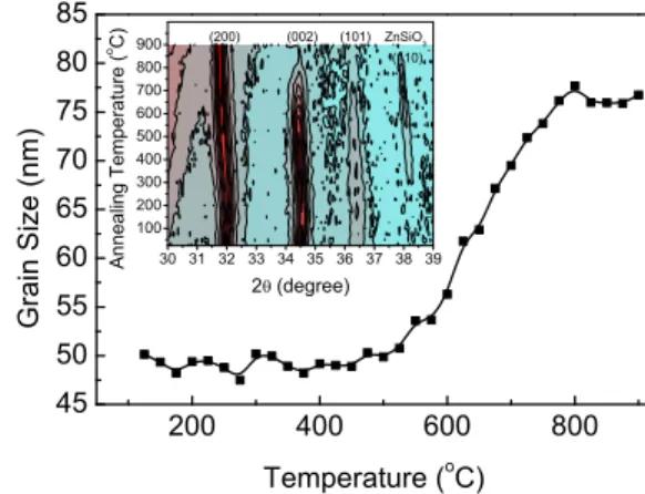
Figure 1 shows the distribution of estimated grain size for varied annealing temperature, deduced from the Scherrer equation,
Dhkl=
cos,
in which is the shape factor-about 0.89, is the x-ray wavelength—1.55 Å in this experiment,is the full width at
a兲Author to whom correspondence should be addressed. Electronic mail:
FIG. 1.共Color online兲 Distribution of grain size with annealing temperature as shown in the figure and inset from in situ XRD mapped, which shows a preferred orientation as temperatures greater than 800 ° C and a ZnO/Si interface compound formation from 300 to 800 ° C.
APPLIED PHYSICS LETTERS 97, 181915共2010兲
0003-6951/2010/97共18兲/181915/3/$30.00 97, 181915-1 © 2010 American Institute of Physics This article is copyrighted as indicated in the article. Reuse of AIP content is subject to the terms at: http://scitation.aip.org/termsconditions. Downloaded to IP:
half maximum 共FWHM兲 in the angular width of the maxi-mum intensity of a diffraction feature 共hkl兲, is the Bragg angle and Dhklis the grain size or average distance of grain
boundary along direction 共hkl兲. The grain size remained al-most constant for an annealing temperature from 25 to 500 ° C, but above 500 ° C the grains began to grow and to attain a saturated value of⬃77 nm at 800 °C. In addition, Bragg peaks 共002兲 and 共101兲 had decreasing intensity with increasing annealing temperature, and disappeared for an-nealing temperature above 800 ° C as shown in the inset of Fig. 1. The orientation of grains in ZnO films altered from random to preferred 共200兲 on annealing at 800 °C, and the intensity of the 共200兲 diffraction signal quadrupled from the value for the sample as grown; these results indicate that crystallites with the c-axis parallel to the growth direction lie along the sample surface. In situ XRD showed an extra fea-ture located at 2⬃38° that appeared from 300 to 850 °C. According to the results of our XRD refinement, this feature originated from a共110兲 Bragg peak of zinc silicate, ZnSiO3. The temperature of formation of this ZnSiO3 phase was ⬃100 °C less than reported.11The low-temperature PL
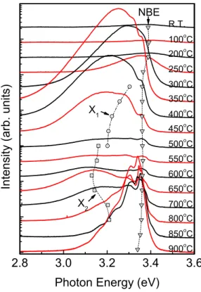
spec-tra for varied annealing temperature show in Fig.2two extra emission lines with labels X1 and X2; open circles and squares with a dashed line indicate the fitted results of posi-tions from 3.1 eV to 3.3 eV. The temperature distribuposi-tions of X1 and X2 are the same as those of the formation of a ZnSiO3 phase shown in XRD patterns 共Fig. 1兲. The NBE position marked with open triangles and a labeled dashed line showed a red-shift behavior for annealing temperatures from 25 to 900 ° C. To verify the formation of the ZnSiO3 phase at the interface, we grew an amorphous buffer layer of Al2O3 on Si at 25 ° C with 20 ALD cycles yielding a thickness of 2 nm before deposition of the ZnO thin film.
Figure 3 show the PL spectra of ZnO thin films with and without the Al2O3 buffer layer. The feature located at 3.13 eV and related to the ZnSiO3phase vanished with this Al2O3 buffer layer sample, and the emission band at 3.3 eV called D-band emission was also observed with annealing tempera-ture 850 and 900 ° C, shown in Fig.2, accompanied with two phonon replicas. The existence of such optical-phonon replicas was also reported by Makino et al.12 This feature might be attributed to a piezoelectric, spontaneous polarization effect, or a donor-acceptor pair 共DAP兲 from an alloyed layer. As the Al–O bond energy共511 kJ/mol兲 is much larger than the Zn–O bond energy共271 kJ/mol兲 and the Si–O bond energy 共452 kJ/mol兲, it is reasonable to assume that Si–O and Zn–O bonds are much more difficult to break and to react with each other across an Al2O3 layer. Furthermore, the Al2O3 buffer layer provided interdiffusion blocking to avoid the recombination path of a non-UV region from the interface, and improved the optical efficiency of Si-based UV devices. Figure 4共a兲 shows the NBE energy and inte-grated NBE intensity with varied annealing temperature. The NBE energy decreased from 3.39 to 3.36 eV at 200 ° C then increased slightly to 3.365 eV at 550 ° C, and finally ap-proached 3.34 eV at 800 ° C with increasing annealing tem-perature. In contrast, the NBE intensity rose and fell as its energy decreased and increased respectively. To understand the behavior of the optical response of a n-ZnO/p-Si 共111兲 heterojunction, we applied a secondary-ion mass spectrom-eter共SIMS兲 analysis of the distribution of composition of the thin film. The filled squares in Fig. 4共b兲 show the average intensity of hydrogen concentration of the entire film. The results indicate that the hydrogen intensity decreased⬃80% for temperatures from 200 to 400 ° C; ⬃18% of hydrogen was recovered at 500 ° C. This behavior was observed also on annealing the hydrogen free-carrier absorption in ZnO.13 The hydrogen concentration showed similar trends with the FIG. 2.共Color online兲 Photoluminescence spectra of n-ZnO/p-Si共111兲 with
thermal treatment from 100 to 900 ° C. Inset—dashed lines with symbols indicated the positions of lines of NBE, X1 and X2 emission band, respectively.
FIG. 3. 共Color online兲 Comparison of photoluminescence spectra of
n-ZnO/p-Si共111兲 and n-ZnO/Al2O3/p-Si共111兲 with a 2 nm Al2O3 inter-layer; the annealing temperature is 500 ° C.
181915-2 Ku et al. Appl. Phys. Lett. 97, 181915共2010兲
This article is copyrighted as indicated in the article. Reuse of AIP content is subject to the terms at: http://scitation.aip.org/termsconditions. Downloaded to IP: 140.113.38.11 On: Wed, 30 Apr 2014 09:55:58
NBE energy. The peak position of NBE proved the Burstein– Moss effect.14 The hydrogen atoms hence act as a shallow donor state in the thin film in agreement with the theoretical work by Van de Walle.15 The NBE intensity of PL spectra also varied with the hydrogen concentration because of impurity doping that induced a sizable increase of the non-radiative trap center concentration.16 We observed a broad-ening of lines on NBE with respect to hydrogen concentra-tion shown in Fig.4共b兲; this effect was observed on a heavily doped n-type carrier system such as Ga-doped ZnO films.17 The growth of a thin film of ZnO at 25 ° C containing a large concentration of H+might result from surface absorption of molecular H2O during ALD. In our case, the excess water pulsed into the chamber to ensure the completed reaction between the DEZn precursor and water excludes the possi-bility of oxygen vacancy. Water is difficult to eliminate from a vacuum system at such a low temperature of growth when the purge gas begins to clear the chamber and the sample surface. A preceding adsorption result18 indicates that a lower temperature of pretreatment yields more homotattic hydroxylate sites on the ZnO surface, which means that the close-packed surface hydroxyl groups bonded to the ZnO surface result from the formation of mutual hydrogen bond-ing. We propose that the abundant concentration of the H+ state via hydroxyl groups remains even after finishing our ALD processes. Also according to DFT calculations,15 hydrogen is difficult to remove from the crystal matrix. The strong bonds between oxygen and hydrogen atoms also provide a powerful driving force for its incorporation into the ZnO crystal. In this way, there are four possible positions–BC⬜, BC储, AB0,⬜, and AB0,储, with formation ener-gies Ef ⫺1.84 eV, ⫺1.82 eV, ⫺1.78 eV, and ⫺1.59 eV,
respectively.15 The negative formation energy indicates a stable state in the crystal. In our present work,19the PL of a ZnO thin film grown on 共0002兲 sapphire near 100 °C also showed greater PL intensity; the reason is that evaporation of surface water at the boiling point decreases the hydrogen contamination in the thin film and enhances the optical emis-sion, although showing a satisfactory crystalline quality at lower temperatures of growth.
In summary, we have presented the effect of annealing on the photoluminescence and structural properties of ZnO films prepared with the ALD technique. We grew a polycrys-talline ZnO thin film on Si共111兲 at 25 °C that showed 共200兲 preferential orientation after thermal annealing over 800 ° C; the average grain size grows⬃50% from 50 to 77 nm. The NBE intensity of the PL was significantly enhanced by this annealing, and this enhancement correlates with the concen-tration of residual hydrogen in the ZnO films. An ultrathin Al2O3 layer can serve effectively to block interdiffusion to avoid the X1and X2emission signals from formation of the ZnSiO3 phase at the interface. A greater temperature of the substrate or annealing after growth proved an effective way to decrease the concentration of n-type free carrier from doped hydrogen and obtain improved quality of PL for the ALD method.
National Science Council of the Republic of China, Taiwan, provided support under Contract Nos. NSC 98-2221-E-213-002, NSC 97-2112-M-134-001-MY2, and NSC 97-2120-M-001-007.
1C. S. Ku, H. Y. Lee, J. M. Huang, and C. M. Lin,Cryst. Growth Des. 10,
1460共2010兲.
2H. Paul Maruska, F. Namavar, and N. M. Kalkhoran,Appl. Phys. Lett.61,
1338共1992兲.
3H. Ohta, M. Orita, M. Hirano, and H. Hosono,J. Appl. Phys. 89, 5720
共2001兲.
4Ya. I. Alivov, J. E. Van Nostrand, D. C. Look, M. V. Chukichev, and B. M.
Ataev,Appl. Phys. Lett. 83, 2943共2003兲.
5Ya. I. Alivov, E. V. Kalinina, A. E. Cherenkov, D. C. Look, B. M. Ataev,
A. K. Omaev, M. V. Chukichev, and D. M. Bagnall,Appl. Phys. Lett. 83,
4719共2003兲.
6C. Yuen, S. F. Yu, S. P. Lau, and T. P. Chen,Appl. Phys. Lett. 86, 241111
共2005兲.
7W. I. Park and G. C. Yi,Adv. Mater. 16, 87共2004兲.
8D. C. Look, B. Claflin, Ya. I. Alivov, and S. J. Park,Phys. Status Solidi A
201, 2203共2004兲.
9C. G. Van de Walle and R. A. Street,Phys. Rev. B 51, 10615共1995兲. 10C. S. Ku, J. M. Huang, C. M. Lin, and H. Y. Lee,Thin Solid Films 518,
1373共2009兲.
11X. L. Xu, P. Wang, Z. Qi, H. Ming, J. Xu, H. Liu, C. S. Shi, G. Lu, and W.
K. Ge,J. Phys.: Condens. Matter 15, L607共2003兲.
12T. Makino, K. Tamura, C. H. Chia, Y. Segawa, M. Kawasaki, A. Ohtomo,
and H. Koinuma,Appl. Phys. Lett. 81, 2172共2002兲.
13G. A. Shi, M. Stavola, S. J. Pearton, M. Thieme, E. V. Lavrov, and J.
Weber,Phys. Rev. B 72, 195211共2005兲.
14E. Burstein,Phys. Rev. 93, 632共1954兲.
15C. G. Van de Walle,Phys. Rev. Lett. 85, 1012共2000兲.
16H. J. Ko, Y. F. Chen, S. K. Hong, H. Wenisch, T. Yao, and D. C. Look, Appl. Phys. Lett. 77, 3761共2000兲.
17T. Makino, Y. Segawa, S. Yoshida, A. Tsukazaki, A. Ohtomo, and M.
Kawasaki,Appl. Phys. Lett. 85, 759共2004兲.
18M. Nagao,J. Phys. Chem. 75, 3822共1971兲.
19C. S. Ku, H. Y. Lee, J. M. Huang, and C. M. Lin,Mater. Chem. Phys. 120,
236共2010兲. FIG. 4. 共a兲 Filled squares indicate the NBE emission energy and open
squares show how the intensity varies with annealing temperature.共b兲 Filled and open squares show the concentrations of hydrogen and boron atoms, respectively.
181915-3 Ku et al. Appl. Phys. Lett. 97, 181915共2010兲
This article is copyrighted as indicated in the article. Reuse of AIP content is subject to the terms at: http://scitation.aip.org/termsconditions. Downloaded to IP: 140.113.38.11 On: Wed, 30 Apr 2014 09:55:58