Invited Paper
Arsenic-Implanted
GaAs: An Alternative Material to
Low-Temperature-Grown GaAs for Ultrafast Optoelectronic Applications
Ci-Ling Pan and Gong-Ru Lin
Institute of Electro-Optic Engineering, National Chiao Tung University Hsinchu, Taiwan 30010, Republic of China
Abstract
Arsenic-ion-implanted GaAs (or GaAs:As), with excess-arsenic-related deep level
defects, has recently emerged as a potential alternative to low-temperature
molecular-beam-epitaxy (LTMBE) grown GaAs for ultrafast optoelectronic applications. In this paper, we review results of our structural, ultrafast optical and optoelectronic
investigations of as-implanted and thermally annealed GaAs:As. Picosecond
photoconductive switching responses are reported for devices fabricated on
thermally-annealed low-dose and high-dose implanted GaAs:As. Novel sign reversals in
near-bandgap ultrafast optical responses were observed and explained.
Keywords: arsenic-ion-implanted GaAs, GaAs:As, ultrafast, photoconductive switch
I. Introduction
Photoconductors with ultrashort photo-excited carrier lifetime, good optical
responsivity, high breakdown field and low dark current are essential for ultrafast optoelectronic switching applications. Various classes of semiconductors, e.g., intrinsic, impurity-dominated, radiation-damaged, polycrystalline, and amorphous, have been explored as ultrafast photoconductors. In particular, the ion implantation technique has been employed extensively. Carrier lifetimes as short as 0.5
O.6
pshave been reported as the saturation limit for GaAs samples irradiated by protons (H)
and oxygen-ion-implanted silicon-on sapphire (SOS) materials. On the other hand,
nonstoichiometric, arsenic-rich GaAs grown by molecular beam epitaxy (MBE) at low substrate temperature (LT-GaAs) have been the subject of intensive studies because of its nearly ideal electrical and optoelectronic properties. Appropriate annealing of the material is required, however. Recently an alternative rich-material,
optoelectronic applications. The structural and electrical characteristics of LT-GaAs and GaAs:As have been shown to be quite similar. Subpicosecond carrier lifetimes
[1,2] and photoconductive responses [3] comparable to that of LT (low-temperature)
MBE-grown GaAs were reported. In this work, we review structural, electrical and ultrafast optical properties of furnace-annealed GaAs:Ast Ultrafast photoconductive
switches fabricated on furnace-annealed GaAs:As were demonstrated.
II. Sample Preparation and Experimental Methods
The samples were prepared by first implanting semi-insulating GaAs substrates with 200 keV arsenic ions at a dose of 1016 ions/cm2 and then furnace-annealed ex-situ
between Ta 200 and 800 °C for 30 minutes. The effect of the furnace annealing
process on the structural properties of Astimplanted GaAs was examined by x-ray
rocking curve and transmission electron microscopy (TEM) measurements. For
electrical characterizations of the arsenic-ion-implanted GaAs subatrates, shottky diodes with thermally evaporated gold (0.5 mm thick) contacts were fabricated. Their current voltage (I-V) performance was measured by using a semiconductor parametric analyzer (HP4145B). Carrier lifetimes and transient indices of refraction
of the annealed samples was measured by using a standard pump-probe system with a
time resolution of about 130 fs. Photoconductive switches (PCS) with coplanar
stripline structures were fabricated on samples annealed at 600°C. The choice of this
annealing condition was based on good crystallinity, excellent dark resistivity and
ultrafast carrier lifetimes as determined by structural, electrical, and optical
characterization of the samples. These devices were then characterized by anexternal electro-optic sampling (EOS) system. The temporal and spatial resolutions
of the EOS system are approximately about 1 Ps and 5 mm,respectively.
III. Structural and Electrical Properties
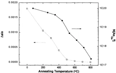
The deviation of the lattice constant Aa and the related vertical strainparameter
AaJa of GaAs:As furnace-annealed at various temperatures were determined from
X-ray data, These are shown in Fig. 1. For the as-implanted sample, the maximum
vertical strain, AaIa 0.35%, is located at about 0.09 mm below the surface. In
and a =
5.6595.66OA) for LT-GaAs (growth temperature 200 °C ). As theannealing temperature is increased from Ta 200 °C ,weobserved that the X-ray side-peak gradually shifted toward and merged with the central side-peak for Ta>500 °C . In
comparison, the side-peak for LT-GaAs merged with the main peak at a lower
annealing temperature of 450°C. That is, the rate of recovery for crystallinity of GaAs:As is somewhat slower than that of LT-GaAs grown by MBE. The critical annealing temperatures for the complete recovery of crystallinity of Ask-implanted
GaAs is estimated to be higher than Ta 500 °C.
The density of the neutral ASGa antisite [A5Ga0] defects responsible for the
trapping of photoinjected carriers has also been evaluated. From experimental
values of N[A5G°] for the as-implanted Ask-implanted GaAs (1O20 cm3) and S.I. GaAs substrate (IO16 cm3) determined previously by our group.[6,7] We estimate
that N[A5Ga0 5.56x10²²(AaJa) for GaAs:Ast The proportional constant is slightly
smaller than that for LT-GaAs (5.56x 10²²). It may be explained by the relatively poor crystallinity of GaAs:As prepared by as compared with that in LT-GaAs. Thus it requires higher annealing temperature to recover the crystallinity. As a supporting
evidence, the N[A5Ga0] ofthe GaAs:As sample annealed at temperature of 600 °C was in reasonably good agreement with previous results of 3x 1 18cm3obtained from the
capacitance-voltage measurement.[8] A comparison of the structural and electrical properties of furnace-annealed GaAs:As and related materials are summarized in
Table 1.
Iv. Ultrafast Optical properties
Previously, we have reported subpicosecond photoexcited carrier lifetimes (-ce)
ranged from 0.19 ps to 0.28 ps in GaAs implanted with 200 KeV arsenic ions at
12 16. 2 +
dosages from 10 to 10 ions/cm .[1] For RTA-annealed GaAs:As at 600 C to 800 °C, -re's from 0.48 to 2.3 ps were observed.[2] From results of femtosecond time-resolved reflectivity measurements (see Fig. 2), we find that photo-excited carrier lifetimes of furnace-annealed GaAs:As were in the range of 0.4 to 4.6 Ps (200°C Ta 800°C) with an approximate (Ta)4 dependence. This is also shown in
Fig. 3 . ForTa 500 °C, t's evolved slowly with increasing Ta and were all in the subpicosecond range. The corresponding changes of the refractive index, An, were
of the order of -2 to -3 x 1 O .
A
novel sign reversal for An was observed for 600°CTa 700°C. The peak magnitude of n was as large as 0.01 at Ta 700°C. This
can be explained if the bandgap of GaAs:As shrinks due to bandgap renormalization toward shorter wavelength after annealing. This is in agreement with results of the cw photoreflectance experiment. The ultrafast carrier lifetimes are consistent with
structural characterization of GaAs:As that demonstrated ultrahigh densities of defect
states present in the samples annealed at these temperatures. The density of neutral
ASGa antisite defects was determined to be 2 X l0 cm3 at Ta800°C. Effective captured cross-section of the photo-excited carriers for the GaAs:As samples
annealed at different temperatures were evaluated by using Schkoley-Read-Hall model and listed in Table 1 . Arsenicprecipitates, however, were not observed for Ta 600 OC . This suggests that arsenic clusters were not as important for the ultrafast carrier
trapping process in GaAs:As as for LT-GaAs. See also Table 1 for a comparative
listing of ultrafast optical properties of GaAs:As.
V. Ultrafast Optoelectronic Applications
Fig. 4 shows the photoconductive response of a furnace-annealed GaAs:As1 PCS.
The duration of the electrical pulse generated by the photoconductive switch was 4 PS. The risetime (1 0% -90%) and l/e falitime were respectively 2 ps and 3 Ps.
These results were measurement-system limited. We estimated the actual response
to be
2 ps, consistent with a photo-excited carrier lifetime of 1 .8 ps. Incomparison, Wang et al.[3] has reported a similar result that the response time of the
similar device fabricated on same material RTA-annealed at 600 °C for 1 5 seconds
was measured to be of 1.23 ps (FWHM). The dark current of an Auston-type
GaAs:As PCS with a
gap size of 30 mm fabricated on the same substrate wasmeasured to be as low as 5nAat 40 volts. The applied electric field at this bias was estimated to be about 15 kV/cm. In comparison, the dark current of an S.I. GaAs based PCS is >10 nA at the same bias. With an injected optical average power of
100 mW (pulse mode) and 3 mW (CW mode) while biased at 20 volts, the
than 0.03 A/W, respectively. This is a few times larger than the responsivity of
LTMBE-GaAs PCS's. This can be attributed to the contribution from bulk material of much larger mobility since the thickness of the implanted layer was too thin to
absorb the injected photons entirely. The performance of GaAs:As PCS's as
compared with that of LT-GaAs PCS are listed in Table 2. We have also recently
reported picosecond responses from low-dose-implanted GaAs:As.[1 0]
VII, Conclusions
In conclusion, we have performed extensive material and device characterization
of a new optoelectronic material, furnace-annealed GaAs:As. The effect of thermal annealing on the key parameters of this material are listed in Table 1 . Current-voltage analysis of the shottky diodes on samples annealed at different temperatures reveals that the optimal annealing temperature for obtaining highly resistive substrate
should be at between 500'600 °C . Thephoto-excited carrier lifetimes were found to increase from 0.26 to 4.6 Ps as Ta was increased up to 800 °C . Signreversal in zn
was observed and explained. Auston-type PCS fabricated on the
optimal-conditioned substrate was measured to be 34 ps by using an external electro-optic sampling system. The performance of GaAs:As as compared with that of 5.1. GaAs and LT-GaAs are listed in Table 2. We showed that arsenic-ion-implanted GaAs
could be a potential useful and alternative material to LT-GaAs for ultrafast optoelectronic applications. This work was supported in part by the National
Science Council of the Republic of China.
References
1 . F. Ganikhanov, G.-R. Lin, W.-C. Chen, C.-S. Chang, and C.-L. Pan, Appi. Phys. Lett. 67, 3465 (1995).
2. G.-R. Lin, W.-C. Chen, C.-S. Chang, and C.-L. Pan, ibid., 69, 996 (1996). 3. H. H. Wang, P. Grenier, J. F. Whitaker, H. Fujioka, J. Jasinski, and Z.
Lilienthal-Weber, IEEE J. Sel. Top. Quantum. 2, 630 (1997).
4. H. Fujioka, J. Krueger, A. Prasad, X. Liu, E. R. Weber, and A. K. Verma, J. Appi. Phys. 78, 1470 (1995).
Wa!ukiewicz, "Native point defects in low-temperature-grown GaAs", App!. Phys. Lett. 67, 279 (1995).
6. G.-R. Lin, W.-.C. Chen, C.-S. Chang, and C.-L. Pan, Appi. Phys. Lett, 65, 3272 (1994).
7. C. -
L.Pan, H. -H.Wu, and T. -R.Hsieh, Jpn. J Appi. Phys. 30, Pt. 1, 1430 (1991).8. W.-C. Chen and C.-S. Chang, App!. Phys. Lett. 68, 646 (1996).
9. H. Shen, Y. Jin, G. A. Wagoner, X.-C. Zhang, and L. Kingsley, Ultrafast Phenomena IX, Springer Series in Chemical Physics, 60, 372, Springer-Verlag Berlin Heidelberg (1994).
10. G.-R. Lin, and C.-L. Pan,Appl. Phys. Lett., 71, 2901 (1997).
Table 1.
The structural and electrical characteristics of GaAs:As samples annealed at
differenttemperatures. as-implant. j 200 °C 400 °C 600 °C 800 O 4AaJa N[AsGaI(cm3) 1.8e-3 j 1.06e-3
1e20
5.9e19 4e-4 2.2e193.79e-5
2'3e18
<3.8e-62e17
DAS(nm) - - -23
20 Iciark(nA/mm2) 1 20.6
0. 1 2 5 .2e-5_
3
.3 'r(ps)0.260.3
0.40.42
0.580.6
1.61.9
424.6
An(x102)(x10 cm )
-0.11-0.130.19
-0.26-0.33 '—0.21 -0.12-0.18'0.39
-0.27-0.32l.5
O.850.976
Table 2.
The performance of GaAs:As PCS samples and related devices.
Performance LT-GaAs GaAs:As GaAs:As
Sample condition 200 °C grown
1 o',
RTA 1016, furnace20 mmgap 30 tm gap 30 tm gap
Dark current <1 tA (10 volts) 3OmA (40 volts) 5 nA(40 volts)
Switching Response 1 .6 Ps 2.7ps 4 Ps
Optical responsiivity 0.001 AIW 0.007 AIW 0.004 A/W
Table 3.
The characteristics of S.l. GaAs, LT-GaAs, and GaAs:As materials.
s.I. GaAs LT-GaAs GaAs:As
Condition LEC Furnace-annealed Furnace-annealed
600°C, 30 mm 600°C, 30 mm
TEM, As-cluster No 6-60 nm 2-3, 20-30 nm
TEM, trap — < 2.83x10'3cm2 O.7-2x1014 cm2
TDC, Ea
0.75 eV0.64 eV
0.6 eV
Ntrap < 2x16 cm3 > 1x 1 9 cm3 2x 1 8 cm3
0.0020 0.0015 m 0.0010
.
0.0005 0.0000 0 200 400 600 800 Annealing Temperature (°C)Fig.1 The vertical strain and associated arsenic antisite defect density as a function of annealing temperature.
0 10 20 30 40
Delay time (ps)
Fig.2The transient reflectivity of GaAs:As samples annealed at different temperatures. o NN 0 1E20 1E19 1E18 1E17 z C) ..9 (f) 600°C w N E 0
z
(b) 200°CU) 4) E 4)
Z2
4) 0 0 > w E w > C) 5 4 ......
•..
S 0 0 1x10¹¹ 2x10¹¹ 3x10¹¹ 4x10¹¹ TFig.3 The carrier lifetime of GaAs:As samples annealed at different temperatures as a function of T4. 2.0x10³ 1.5x10³ 1.0x10³ 5.OxlO 0.0 -5.0x10 -10 30 Delay time (ps)
Fig.4The switching response of 600 °C -annealed GaAs:As PCS measured by using external electro-optic sampling.