www.MaterialsViews.com
COMMUNICA
TION
Ya-Ping Chiu , * Yu-Ting Chen , Bo-Chao Huang , Min-Chuan Shih , Jan-Chi Yang , Qing He ,
Chen-Wei Liang , Jan Seidel , Yi-Chun Chen , Ramamoorthy Ramesh , and Ying-Hao Chu
Atomic-Scale Evolution of Local Electronic Structure Across
Multiferroic Domain Walls
Prof. Y.-P. Chiu , Y.-T. Chen , B.-C. Huang , M.-C. Shih Department of Physics
National Sun Yat-sen University Kaohsiung 80424, Taiwan E-mail: [email protected] J.-C. Yang , C.-W. Liang , Prof. Y.-H. Chu
Department of Materials Science and Engineering National Chiao Tung University
Hsinchu, 30010, Taiwan Q. He , J. Seidel , Prof. R. Ramesh Department of Physics University of California
Berkeley, Berkeley, CA 94720, USA Prof. Y.-C. Chen
Department of Physics
National Cheng Kung University, Tainan 70101, Taiwan
DOI: 10.1002/adma.201004143
In complex, correlated oxides, heterointerfaces have emerged as key focal points of current condensed matter science. [ 1–3 ] For ferroic oxides, in order to minimize the total energy, domain walls emerge as natural interfaces. Multiferroic materials show a wealth of controllable multiple ferroic order through stress, optical excitation, electric, or magnetic fi elds in the same phase, which in turn suggest potential applications in the realization of oxide-based electronic devices, such as spintronics, informa-tion storage devices, or communicainforma-tions. [ 4–7 ] According to the detailed classifi cation given by Mermin in ferroic systems, [ 8 ] domain walls in ferroic systems are considered as two dimen-sional (2D) topological defects, which play an important role in determining the functionality in materials with long-range order. Recently, several key studies pointed out interesting observations on domain walls in multiferroics. [ 9–13 ] For example, Y. Tokunaga et al. showed that ferroelectric polarization and magnetization are successfully controlled by magnetic and electric fi elds in
GdFeO 3 , respectively, which is attributed to the unique feature
of composite domain wall clamping. [ 14 ] T. Choi et al. observed insulating interlocked ferroelectric and structural antiphase domain walls in a multiferroic YMnO 3 system. [ 15 ] H. Bea et al. pointed out that domain walls are the source of the exchange bias interaction between the ferromagnetic metal layer and mul-tiferroic BiFeO 3 (BFO). [ 16 ] Additionally, L. W. Martin further
con-fi rmed that as-grown 109 ° domain walls in BFO thin fi lms are
the contribution for uncompensated spins. [ 17 ] In addition to the above, a very recent work has established electrical conductivity at written multiferroic domain walls in BFO at room tempera-ture, which opens up a pathway by which to manipulate domain walls for next generation nanoelectronics.
Exploring details on electronic states of domain polarization reorientations is critical in oxide multiferroic materials. Theo-retically, the consideration of the evolution of the polarization
across the 109 ° domain walls exhibits a large potential step. The
prediction correlates with the enhanced electrical conductivity due to the generation of a space-charge layer for screening the potential discontinuity in the region of the wall. [ 2 ] Experimentally, conductive atomic force microscopy (c-AFM) studies show the
occurrence of electrical conduction at 109 ° domain walls within
the limited spatial resolution of the experimental technigue. [ 3 ] In spite of the critical importance of these discoveries at such an oxide interface, there have been no effectively direct investi-gations of the intrinsic evolution of the electronic properties at regions of domain walls specifi cally within the nanoscale.
In this work, we explore the subject by measuring the local electronic structure using scanning tunneling micro-scopy (STM) in a cross-sectional geometry. STM and scan-ning tunneling spectroscopy (STS) studies provide direct experimental insight into the origin and nature of the observed electronic conductivity at ferroelectric domain walls in BFO with atomic resolution. Tunneling current–voltage character-istics reveal electronic properties at domain walls, involving a decrease in the local bandgap and built-in asymmetrical poten-tial barriers at domain walls.
Rhombohedral BFO has the ferroelectric polarization
pointing along one of the eight pseudocubic < 111 >
direc-tions, suggesting angles of 71 ° , 109 ° , or 180 ° between allowed polarization directions. In order to investigate intrinsic elec-tronic behaviors, we study the local density of states of as-grown domain walls, instead of written domain walls. Two
types of equilibrium 2D arrays of domain walls, 71 ° and 109 ° ,
were created by careful control of the elastic and electrostatic boundary conditions of the fi lms. [ 18 ] Figure 1 shows the top-view AFM topography (TOPO), the out-of-plane (OOP) and
Figure 1 . The AFM TOPO image, the OOP piezoresponse force images,
the IP piezoresponse force images, and the current mappings measured by tunneling AFM (TUNA) for a) 109 ° and b) 71 ° domains.
www.MaterialsViews.com
COMMUNICA
TION
109 ° domain walls at the cleaved surfaces. Figure 2 c,d depicts
typical topographic images of the 71 ° and 109 ° domain wall in
constant current mode, where the distance between the tip and
sample was stabilized at scanning parameters of + 3.5 V and
1.2 nA. The corresponding electronic structure of the as-grown
71 ° and 109 ° domain walls are displayed in Figure 2 e,f.
Com-bining the topographic images with the corresponding elec-tronic images facilitates the determination of the location of the
domain walls.
Maps of the tunneling conductance were recorded simulta-neously with the topographical images by varying the sample
bias V s and acquiring the differential tunneling current (d I /
d V ) characteristics as a function of the sample bias using lock-in detection. For each spectrum, the feedback loop was turned
off and the sample voltage ( V s ) was ramped between present
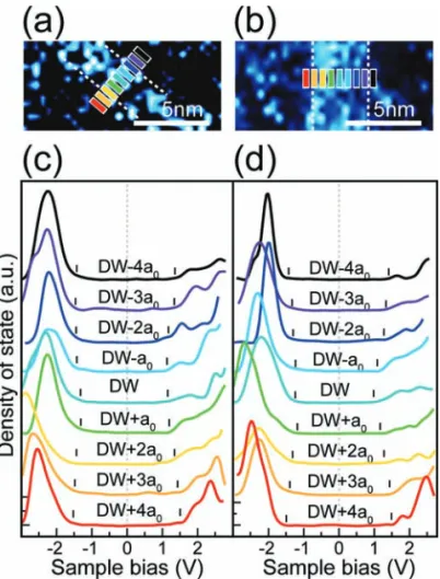
voltages. Scanned with fi xed lifting height and sample bias, domain walls are imaged as bright bands in the electronic struc-ture images, showing higher tunneling conductance than the domain area. Spectral analysis of the sequentially layered elec-tronic characteristics across the domain walls provide insight into the increase in tunneling current, as shown in Figure 3 . Figure 3 presents and shows the analysis of several detailed experimental spatial spectroscopic measurements through
71 ° and 109 ° domain walls. Several colored solid bars in the
atomic-resolution electronic image of the walls in Figure 3 a,b indicate the spatial positions, and the corresponding spectra are shown in Figure 3 c,d. The resulting tunneling spectra in Figure 3 c,d are plotted as the differential tunneling current d I /d V as a function of the sample bias across the domain walls. In a in-plane (IP) piezoresponse force microscope (PFM) mappings
and c-AFM images of 109 ° and 71 ° domains. In addition, more
detailed information on the phase–amplitude combined images is available in previous work. [ 18 , 19 ] During the PFM measure-ments, the cantilever is scanned along the [110] direction. The contrast shown in the OOP and IP images reveal the polari-zations within the domains and thus determine the domain wall types. From c-AFM images, the local conductivity was confi rmed at the domain walls, which rules out that charge accumulation during switching process is the source of this
conducting behavior. The current levels at 109 ° domain walls
(5 pA at 1.6 V) are considerably higher than the current levels at
71 ° domain walls (0.2 pA at 2.2 V), which suggests that the local
properties are different for different types of domain walls. To explore the fundamental mechanism of this conduction, STM was applied to study the detailed electronic structure at
the domain walls. 71 ° and 109 ° domain wall confi gurations
were identifi ed by their well-defi ned geometrical orientation within ordered wall arrays and their local electronic structure, as shown in the sketches in Figure 2 a,b. [ 20 ] In principle, the
orien-tation of 71 ° domain walls, where the adjacent electric
polariza-tions changed from the [–11–1] direction to [–1–1–1], exhibited
a 45 ° tilt angle with respect to the interfacial boundary of BFO/
Nb-STO (pseudocubic (001) plane), as examined in the (0–10)
plane. By contrast, the orientation of 109 ° domain walls, which
are located between the [–111] and [–1–1–1] polarizations, are perpendicular to the interfacial boundary of BFO/Nb-STO, as viewed in the (0–10) plane. These distinct and well-defi ned
dif-ferences in domain wall orientation allow us to identify 71 ° and
Figure 2 . Schematic of the a) 71 ° and b) 109 ° domain-wall arrays. Topographic images of the c) 71 ° and d) 109 ° domain walls, acquired at a sample bias of –3.50 V. Electronic structures images of the e) 71 ° and f) 109 ° domain walls, acquired at a sample bias of + 2.00 V.
www.MaterialsViews.com
COMMUNICA
TION
region of ≈ 2 nm, corresponding to the theoretical estimation. [ 2 ] It should be noted that the magnitude of the changes in the
bandgap depends strongly on the domain-wall type. For the 71 °
wall, a local band-gap reduction of 0.20 eV, about a 6% decrease of the mid-domain bandgaps, is observed. In contrast, the band
edge had a marked shift at the 109 ° domain wall, and the local
bandgap of 109 ° wall is considerably suppressed. According to
the present STM measurements for the 109 ° domain wall, the
bandgap is 2.4 eV, with a reduction of 0.50 eV or about –17% relative to the bandgap of the normal domain region. The STM experimental results show a more obvious band-gap reduction across domain walls as compared to the ones found in
theoret-ical calculations, e.g., 0.05 eV for 71 ° domain walls and 0.10 eV
for 109 ° domain walls. [ 2 , 3 ] A larger reduction of the electronic
bandgap across the 109 ° domain walls is in good agreement
with the previous experimental results of high electrical con-ductivity of 109 ° domain walls. [ 2 , 3 ]
The changes in the electronic structure due to polarization reorientations could lead to an electrostatic potential step at the domain boundary and therefore infl uence the local mobility of electron and hole pairs, which is the key factor for the recently observed photovoltaic effect in BFO. [ 3 , 22–24 ] Therefore, in the article, the immediate concern is how the polarization reorien-tation across the wall infl uences the electronic properties at the wall. As shown in Figure 4 b, the temperature-dependent
elec-tronic properties in the temperature range of ≈ 100–300 K are
analyzed. The small temperature dependence of the Fermi level relative to the band edges as shown in Figure 4 b implies that in the current STM work, the detected free carriers in BFO mainly arise from the intrinsic valence-to-conduction band transitions. In this case, the Fermi level only shifts relative to the band edge of the order of kT ( k is the Boltzmann constant and T is tem-perature), which is about 0.05 eV in the studied temperature range, and thus these STM results can be classifi ed as intrinsic electronic properties. Consequently, the built-in potential for electrons across the domain walls can be correlated from the variation of the separation between the conduction band and the Fermi level ( E F ). [ 23 ] Since the measured tunneling current is proportional to the density of electrons at the semiconductor surface, a smaller bandgap or a smaller separation between the conduction-band edge and the Fermi level imply a larger car-rier density. Therefore, a prominent reduction of the band-gap
size at 109 ° domain walls implies that the carrier density of the
energy sub-bands near the Fermi level is noteworthy and
sug-gests more electrons accumulate at the 109 ° domain boundary
region. In addition, the factor of higher potential difference
across 109 ° domain walls is attributed to the experimental
evi-dence that the 109 ° domain wall is thicker than the 71 ° domain
wall in the electronic STM images in Figure 2 e,f.
Generally, the offsets of the analyzed layer-by-layer band edges can give insight into the characteristics of the intrinsic carrier density distribution or the electrostatic potential steps across domain walls. With the characteristics of d I /d V curves, shown in Figure 3 , the atomic-scale evolution of local electronic property across domain walls can be quantitatively depicted and directly traced in Figure 4 c,d. The key feature observed is that the change of bandgap is mainly attributed to the shift of the conduction band. The obvious downward shift in the conduction-band edge can be correlated with the band-gap region with zero tunneling current, the approximate
locations of valence-band maximum ( E v ) and conduction-band
minimum ( E c ) are extracted and indicated by tick marks in
Figure 3 c,d. The variations in the band structures at different
sites along the length of the 109 ° /71 ° domain walls attribute to
the fl uctuations in the positions of band edges. Consequently, the variation in the band edge is analyzed from several d I /d V curves on different sites for each domain wall. The
uncertain-ties on each band edge position are ≈ 0.19 and 0.23 eV for 109 °
and 71 ° domain walls, respectively (for more detailed original
data and the determination of the band-gap size from I–V and
d I /d V curves see Supporting Information).
The fact that conduction can be activated at the domain walls of BFO at room temperature evokes considerations for
the changes in bandgap ( E g ) across the domain walls. The local
layer-by-layer bandgap is extracted from the difference between
the conduction ( E c ) and valence band edges ( E v ) of electronic
characteristics for different domain walls. The uncertainty in the local bandgap, corresponding to the standard deviation
from several determinations of the local bandgap, for 109 ° (71 ° )
domain walls is about + /− 0.19 ( + /− 0.23) eV. Figure 4 a reveals a signifi cant decrease in bandgaps at the domain walls from the mid-domain experimental value of ≈ 2.9 eV at 110 K. [ 21 ] The spatial extent of the changes in the local bandgap presents a Figure 3 . Layer-by-layer d I /d V measurements across a,c) 71 ° and b,d) 109 ° domain walls, acquired at ≈ 110 K. Bars in (a,b) denote positions where the electronic spectra are probed, and (c,d) show the corresponding spectrum within the detection limits. The band edges are indicated by black tick marks in (c,d).
www.MaterialsViews.com
COMMUNICA
TION
at the domain boundary is a critical formation mechanism for the observed electric conductivity at the domain walls in BFO fi lms. A shift towards the Fermi level in the band edges leads to an increased carrier density with respect to the signifi cant
electrostatic potential step at the wall. The 109 ° domain walls
exhibit enhanced tunneling current compared to 71 ° domain
walls. This may originate from the freedom of the structural deformations to accommodate the changes in carrier density and bandgaps in the polarization reorientation process. The approach demonstrated here serves as a model technique to understand the electronic structures at the oxide interfaces.
Experimental Section
High-quality epitaxial BFO fi lms ( ≈120 nm thick) were prepared by pulsed laser deposition with high-pressure refl ective high-energy electron diffraction (RHEED) on SrRuO 3 -coated DyScO 3 (110) and Nb-doped
SrTiO 3 (001) substrates for c-AFM and STM, respectively. Details on
control of growth can be found in the published literature. [ 20 ] c-AFM has
been applied to probe the local conduction at as-grown domain walls. For STM studies, experiments were performed in an ultrahigh vacuum (UHV) chamber with a base pressure around 5 × 10 − 11 Torr. The samples
were cleaved in situ along the (010) or (100) planes for investigating domain walls. Such an approach avoids surface contamination of BFO fi lms. The chamber was equipped with a variable temperature STM capable of STS measurements. The tunneling spectra were acquired by using the current imaging tunneling spectroscopy (CITS) mode, where
Fe–O octahedral deformations in the wall region, [ 2 , 25–27 ] leading to the change in Fe–O–Fe band angle and the surroundings of minority-spin Fe 3d states at the domain wall. This difference originates from the polarization discontinuity at the boundary of the domain. The visualized atomic-scale band alignment pro-vides a direct portray of how the band structures evolve across the domain walls. Figure 4 c,d show that the band edges have asymmetric magnitudes for domains adjacent to different sides
of the 71 ° or 109 ° domain wall. According to the STM
measure-ments, the shift of the conduction-band and valence-band edges
for successive domains across the 71 ° (109 ° ) wall are about
0.15 (0.15) eV, which is larger than that found in theoretical
estimations. [ 2 ] The results observed in STM measurements can
be mainly originated from the oppositely polarization-induced surface potential modifi cation on the successive ferroelectric domain surfaces. [ 28 , 29 ] The magnitude of the modifi cation of the barrier height in the vicinity of the domain wall can also be estimated from realistic parameters in a simple dielectric gap model (polarization P = 60 μ C cm − 2 , the length of the depletion region δ ≈ 0.25 nm, and the dielectric constant ε ≈ 100).
In summary, we have established a method based on STM and STS measurements in cross-sectional samples to directly elucidate the origin and nature of the unusual local electronic conductivity at ferroelectric domain walls in multiferroic BFO. According to the domain wall orientation and temperature-dependent electronic characteristics, a decrease in the bandgap
Figure 4 . a) Local bandgap across domain walls at 110 K. b) Temperature-dependent band edges from 110 to 300 K for 71 ° and 109 ° domain walls and domains, switching from the right side (R) to the left side (L). Atomic-scale evolution of band structure across c) 71 ° and d) 109 ° domain walls at 110 K. The band edges are indicated by red symbols with error bars in (c,d), respectively. The black dashed lines represent the Fermi level.
www.MaterialsViews.com
COMMUNICA
TION
[ 9 ] B. Meyer , D. Vanderbilt , Phys. Rev. B 2002 , 65 , 104111 . [ 10 ] J. Privratska , V. Janovec , Ferroelectrics 1997 , 204 , 321 . [ 11 ] J. Privratska , V. Janovec , Ferroelectrics 1999 , 222 , 23 .
[ 12 ] V. Goltsev , R. V. Pisarev , Th. Lottermoser , M. Fiebig , Phys. Rev. Lett. 2003 , 90 , 177204 .
[ 13 ] M. Mostovoy , Phys. Rev. Lett. 2006 , 96 , 067601 .
[ 14 ] Y. Tokunaga , N. Furukawa , H. Sakai , Y. Taguchi , T. Arima , Y. Tokura , Nat. Mater. 2009 , 8 , 558 .
[ 15 ] T. Choi , Y. Horibe , H. T. Yi , Y. J. Choi , Weida Wu , S.-W. Cheong , Nat.
Mater 2010 , 9 , 253 .
[ 16 ] H. Béa , M. Bibes , F. Ott , B. Dupé , X.-H. Zhu , S. Petit , S. Fusil , C. Deranlot , K. Bouzehouane , A. Barthélémy , Phys. Rev. Lett. 2008 , 100 , 017204 .
[ 17 ] L. W. Martin , Y.-H. Chu , M. B. Holcomb , M. Huijben , P. Yu , S.-J. Han , D. Lee , S. X. Wang , R. Ramesh , Nano Lett. 2008 , 8 , 2050 . [ 18 ] F. Zavaliche , R. R. Das , D. M. Kim , C. B. Eom , S. Y. Yang , P. Shafer ,
R. Ramesh , Appl. Phys. Lett. 2005 , 87 , 182912 .
[ 19 ] F. Zavaliche , S. Y. Yang , T. Zhao , Y. H. Chu , M. P. Cruz , C. B. Eom , R. Ramesh , Phase Transitions 2006 , 79 , 991 .
[ 20 ] Y.-H. Chu , Q. He , C.-H. Yang , P. Yu , L. W. Martin , P. Shafer , R. Ramesh , Nano Lett. 2009 , 9 , 1726 .
[ 21 ] H. Yang , H. M. Luo , H. Wang , I. O. Usov , N. A. Suvorova , M. Jain , D. M. Feldmann , P. C. Dowden , R. F. DePaula , Q. X. Jia , Appl. Phys.
Lett. 2008 , 92 , 102113 .
[ 22 ] S. Y. Yang , J. Seidel , S. J. Byrnes , P. Shafer , C.-H. Yang , M. D. Rossell , P. Yu , Y.-H. Chu , J. F. Scott , J. W. Ager , III, L. W. Martin , R. Ramesh , Nat. Nanotechnol. 2010 , 5 , 143 .
[ 23 ] S. M. Sze , K. K. Ng , Physics of Semiconductor Devices , 3rd ed., John Wiley & Sons, Inc. , Hoboken, NJ 2006 .
[ 24 ] L. Pintilie , C. Dragoi , Y. H. Chu , L. W. Martin , R. Ramesh , M. Alexe , Appl. Phys. Lett. 2009 , 94 , 232902 .
[ 25 ] G. Catalan , J. F. Scott , Adv. Mater. 2009 , 21 , 2463 .
[ 26 ] A. Y. Borisevich , H. J. Chang , M. Huijben , M. P. Oxley , S. Okamoto , M. K. Niranjan , J. D. Burton , E. Y. Tsymbal , Y. H. Chu , P. Yu , R. Ramesh , S. V. Kalinin , S. J. Pennycook , Phys. Rev. Lett. 2010 , 105 , 087204 .
[ 27 ] A. Y. Borisevich , O. S. Ovchinnikov , H. J. Chang , M. P. Oxley , P. Yu , J. Seidel , E. A. Eliseev , A. N. Morozovska , R. Ramesh , S. J. Pennycook , S. V. Kalinin , ACS Nano 2010 , 4 , 6071 .
[ 28 ] P. Maksymovych , S. Jesse , P. Yu , R. Ramesh , A. P. Baddorf , S. V. Kalinin , Science 2009 , 324 , 1421 .
[ 29 ] W. Wu , J. R. Guest , Y. Horibe , S. Park , T. Choi , S.-W. Cheong , M. Bode , Phys. Rev. Lett. 2010 , 104 , 217601 .
a series of tunnel current images was obtained at different sample bias voltage V s . V s in this work was varied from –3.5 to + 3.5 V for STS
measurements. STM and STS images were simultaneously acquired in the ≈ 100–300 K temperature range using the conventional lock-in technique by application of a small ac modulation voltage ( V m = 40 mV,
modulation at ≈ 1.1 KHz) to the sample bias voltage V s . STM combined
with STS facilitates acquisition of relevant information directly on the local electronic structure at domain walls of BFO.
Supporting Information
Supporting Information is available from the Wiley Online Library or from the author.
Acknowledgements
The authors thank the National Science Council of the Republic of China, Taiwan, for fi nancially supporting this research under Contract No. NSC 98 – 2112-M-110 – 005-MY3 and No. NSC 98 – 2119-M-009 – 016. Berkeley group acknowledges support by the Director, Offi ce of Science, Materials Sciences and Engineering Division, of the Department of Energy under contract No. DE-AC02 – 05CH11231. J.S. Acknowledges support from the Alexander von Humboldt Foundation.
Received: November 9, 2010 Revised: December 14, 2010 Published online: February 22, 2011
[ 1 ] A. Ohtomo , H. Y. Hwang , Nature 2004 , 427 , 423 .
[ 2 ] A. Lubk , S. Gemming , N. A. Spaldin , Phys. Rev. B 2009 , 80 , 104110 .
[ 3 ] J. Seidel , L. W. Martin , Q. He , Q. Zhan , Y.-H. Chu , A. Rother , M. E. Hawkridge , P. Maksymovych , P. Yu , M. Gajek , N. Balke , S. V. Kalinin , S. Gemming , F. Wang , G. Catalan , J. F. Scott , N. A. Spaldin , J. Orenstein , R. Ramesh , Nat. Mater. 2009 , 8 , 229 .
[ 4 ] N. A. Spaldin , M. Fiebig , Science 2005 , 309 , 391 .
[ 5 ] W. Eerenstein , N. D. Mathur , J. F. Scott , Nature 2006 , 442 , 759 . [ 6 ] S. W. Cheong , M. Mostovoy , Nat. Mater. 2007 , 6 , 13 .
[ 7 ] R. Ramesh , N. A. Spaldin , Nat. Mater. 2007 , 6 , 21 . [ 8 ] N. D. Mermin , Rev. Mod. Phys. 1979 , 51 , 591 .