國立交通大學
電子工程學系 電子研究所碩士班
碩 士 論 文
非對稱輕摻雜汲極金屬氧化半導體電晶體應用
於2.4GHz之功率放大器
A 2.4GHz CMOS Power Amplifier with Asymmetric-LDD
MOS Transistors
研究生:辜柏翔
指導教授:荊鳳德 博士
非對稱輕摻雜汲極金屬氧化半導體電晶體應用於2.4GHz之
功率放大器
A 2.4GHz CMOS Power Amplifier with Asymmetric-LDD
MOS Transistors
研 究 生:辜柏翔 Student: Po-Hsiang Ku
指導教授:荊鳳德 博士 Advisor: Dr. Albert Chin
國 立 交 通 大 學
電子工程學系 電子研究所碩士班
碩士論文
A Thesis
Submitted to Department of Electronics Engineering & Institute of Electronics College of Electrical and Computer Engineering
National Chiao Tung University In Partial Fulfillment of the Requirements
For the Degree of Master In
Electronics Engineering July 2009
Hsinchu, Taiwan, Republic of China
非對稱輕摻雜汲極金屬氧化半導體電晶體應用於
2.4GHz 之功率放大器
學生:辜柏翔
指導教授:荊鳳德 博士
國立交通大學
電子工程學系 電子研究所碩士班
摘 要
本論文展示一種以非對稱輕摻雜汲極金氧半導體電晶體來製作之 2.4GHz 功 率放大器,它可以用TSMC 0.18μm 的 CMOS 一般製程環境來實現。此非對稱 輕摻雜汲極金氧半導體電晶體擁有的汲極源極崩潰電壓大約為一般電晶體的 2 倍,所以這個設計約可穩定的操作在2.5V~3V,而較高的操作電壓使得電路有優 越的功率。根據模擬的結果,功率增益可以達到26.5dB,輸出功率 P1dB 可以達 到24.9dBm,功率增加效率(PAE)在 P1dB 點可以達到 20%,與超過 40dBm 的輸 出三階互調截點(OIP3)。 未來的製程不斷縮小,降低工作電壓對於功率放大器是很大的設計瓶頸,此 種功率單元的設計方式,將會是製程整合的良好解決方案。A 2.4GHz CMOS Power Amplifier with
Asymmetric-LDD MOS Transistors
Student: Po-Hsiang Ku Advisor: Dr. Albert Chin
Department of Electronics Engineering and Institute of Electronics
National Chiao Tung University
Abstract
This paper presents a 2.4 GHz CMOS power amplifier with asymmetry-LDD transistor and implements in TSMC 0.18μm CMOS technology. The
asymmetry-LDD transistor has about twice drain breakdown voltage to the
conventional transistor, hence the voltage source in the design can supply about 2.5V to 3V. And the power amplifier can achieved higher output power. According to simulation result, the power gain is 26.5dB, output P1dB is 24.9dBm, the PAE at P1dB is 20%, and OIP3 is over 40dBm.
In the future, the low voltage is a bottleneck to power amplifier. So this power cell design might be a solution to integrate RFIC power amplifier into system on chip (SOC) with lower cost.
誌 謝
首先感謝我的指導教授荊鳳德博士,給予我的指導和鼓勵,讓我
在電路設計這一方面學習到很多,也讓我在這兩年的時間裡學習到許
多有關於研究的態度與方法。
同時也感謝實驗室的張慈學長、思麟學長,提供你們寶貴的經驗
與知識給我,讓我了解到更多且給了我很多幫助。
還有一起奮鬥的順芳、冠翰和鉅宗,大家一起研究討論、一起解
決問題,在相互討論之下更是激發了許多靈感。還有學長、學弟的陪
伴,都是我碩士生活中美好的回憶。
還要感謝我的家人,父母給我的栽培與期望,以及哥哥在這段時
間的幫忙,讓我在做研究時,生活沒有後顧之憂,使我能順利完成學
業。
希望各位實驗室的學長、弟、妹,都能順順利利地作好自己的研
究,祝各位前程似錦,一帆風順。
謝謝所有關心我以及陪伴我的人!
辜柏翔
98 年 7 月
Contents
Abstract (in Chinese) ………... i
Abstract (in English) ……….. ii
Acknowledgements ……….... iii
Contents ……….. iv
List of Table ……….... vi
List of Figure ………... vii
Chapter1_Introduction ……….. 1
1.1 RF Transceivers ………... 1
1.2 Motivation ………..……….. 2
Chapter2_Concept of Power Amplifier ………..……….……. 4
2.1 Smith Chart ……….. 4
2.2 Parameter definitions ……….……….. 6
2.2.1 S-parameter ……… 6
2.2.2 Stability ……….. 8
2.2.3 Power gain ……… 11
2.2.4 Output power and P1dB ………... 13
2.2.7 Adjacent channel power ratio (ACPR) ……… 19
2.2.8 Peak-to-Average Ratio (PAR) ……….……..…... 20
2.3 Classification of power amplifier ………..…… 21
2.3.1 Class A, B, AB, and C ………..……… 22
2.3.2 Class D, E and F ………..………. 28
Chapter3_Asymmetric LDD MOS Power Cell ………..…… 31
3.1 Why asymmetric LDD MOS ……….……… 31
3.2 Model building ……….……….. 33
Chapter4_Power Amplifier Design ……….……… 35
4.1 Circuit design ……….…… 35 4.2 Design flow ……….……... 36 4.3 Pre-layout simulation ……….… 38 4.4 Post-layout simulation ………... 47 4.5 Measurement ……….. 54
Chapter5_Conclusion ………... 56
Reference ………....57
List of Table
Chapter 2
Table 2.1:The operation in different mode ………..………... 26
Chapter 4
Table 4.1:The goal of power amplifier ………..………… 38 Table 4.2:The result of power amplifier ………..…... 54
List of Figure
Chapter 1
Fig. 1.1:Transceiver block diagram ………..……….. 1
Chapter 2
Fig. 2.1:Smith Chart ……….………..… 4Fig. 2.2:constant-resistance circles ……….…....……… 6
Fig. 2.3:constant-reactance circles ………..……… 6
Fig. 2.4:Two-port network ………..……… 7
Fig. 2.5:Two-port network stability parameters ……….………… 8
Fig. 2.6:The stable region for ΓL-plane (a) |S11|<1 (b) |S11|>1 ………….……….. 10
Fig. 2.7:The stable region for ΓS-plane (a) |S22|<1 (b) |S22|>1 ………... 10
Fig. 2.8:Different power definitions ……….………. 12
Fig. 2.9:Constant available power gain circles ……….………. 13
Fig. 2.10:1-dB compression point ……….……… 14
Fig. 2.11:A power amplifier diagram ……… 15
Fig. 2.12:IM in a nonlinear system ……….…….. 18
Fig. 2.13:Corruption of a signal due to IM between two interferers ……….……… 18
Fig. 2.14:Growth of output components in an IM test ……….………. 19
Fig. 2.16:The waveform of voltage and current ………..…. 22
Fig. 2.17:The waveform of current ………..……. 24
Fig. 2.18:The bias condition for various classes of power amplifier ………..…….. 25
Fig. 2.19:All components in the current waveform ……….……. 27
Fig. 2.20:RF power and efficiency with conduction angle ……….….. 28
Fig. 2.21:Waveforms of ideal power amplifiers ………...…… 30
Chapter 3
Fig. 3.1:Device structure of asymmetric-LDD MOS ……… 31Fig. 3.2:The drain breakdown voltage at Vgs=0 V with 0.23μm gate length ….….. 32
Fig. 3.3:Measured RF output power and PAE versus the input power for conventional and asymmetric-LDD MOS transistors at 2.4 GHz. ……….. 33
Fig. 3.4:Asymmetric LDD NMOS model ……….…… 34
(a) The BSIM model of A-LDD NMOS (b) The equivalent circuit of A-LDD NMOS
Chapter 4
Fig. 4.1:Schematic of the two stage amplifier circuit ……… 35Fig. 4.2:Design flow chart ………. 37
Fig. 4.3:schematic ……….…… 39
Fig. 4.5:Schematic after input and inter-stage matching ………..…… 40
Fig. 4.6:Schematic of load-pull in ADS ……….... 41
Fig. 4.7:Simulation result of load-pull in ADS ……….……… 42
Fig. 4.8:Load-pull for this PA ……….……….. 42
Fig. 4.9:Ideal lump schematic ……….…….. 43
Fig. 4.10:TSMC model schematic ……….……… 44
Fig. 4.11:S-parameter of pre-layout simulation ……….……… 44
Fig. 4.12:Stability factor of pre-layout simulation ……… 45
Fig. 4.13:Power gain of pre-layout simulation ……….………. 45
Fig. 4.14:Output power of pre-layout simulation ……….………. 46
Fig. 4.15:Power Added Efficiency of pre-layout simulation ……….……… 46
Fig. 4.16:IP3 of pre-layout simulation ……….. 47
Fig. 4.17:Export the line of layout to momentum ADS system and simulation …… 48
Fig. 4.18:Post-layout simulation with line calculation ……….………. 49
Fig. 4.19:The layout after post-layout simulation ……….……… 50
Fig. 4.20:S-parameter of post-layout simulation ……….……….. 51
Fig. 4.21:Stability factor of post-layout simulation ……….……….. 51
Fig. 4.22:Power gain of post-layout simulation ……… 52
Fig. 4.24:Power Added Efficiency of post-layout simulation ……….. 53 Fig. 4.25:IP3 of post-layout simulation ……… 53 Fig. 4.26:The photograph of the chip ……… 55
Chapter 1
Introduction
1.1 RF Transceivers
Over the last few decades, many advances have been made in area of wireless communication technology. Those applications become a part of our live. Such as mobile phone, wireless mouse, keyboard, wireless local area network (W-LAN), notebook, RFID, global positioning system (GPS) etc. In general, communication system can be shown like Fig. 1.1.
Fig. 1.1 Transceiver block diagram
Fig. 1.1 is a transceiver block diagram, a transceiver means a unit which contains both a receiver and a transmitter. Transmitter transmit the signal after digital signal
baseband section. The transceiver is included power amplifier (PA), low noise
amplifier (LNA), mixer, voltage controlled oscillator (VCO), phase locked loop (PLL). Power amplifier is the most important device of transmitter, so this research is focus on the design of PA.
PA has to transmit the signal to the air, so it requires large output power with linearity and efficiency. But it is very difficult for it to increase linearly and efficiency at the same time, that is the reason why discrete or hybrid implementations of this circuit are so popular.
Pseudomorphic High Electronic Mobility Transistor (pHEMT) FET, Hetero-junction bipolar transistor (HBT), bipolar junction transistor (BJT), CMOS, Bi CMOS, LDMOS are common implementation of RF integrated circuit.
Each implementation technology has their advantage and drawback, so it is the reason why individual implementation component built systems are favored for so many years. CMOS for base band section, bipolar for IF partition, ceramic for SAW filters, III-V such as GaAs for RF transmitter especially for power amplifier.
1.2 Motivation
In RF circuit design, PA is the most power-required building blocks. Large supply voltage is necessary condition for practical application. CMOS PA design will face the
great impact and hard to survive in advance technology implementation with low supply voltage.
The RF power performance of Si MOSFET has little improvement with down-scaling, which is limited by the inherent low breakdown voltage. This is especially important for RF PA, where the voltage swing is about twice of DC bias voltage. This restriction decreases maximum output power, power density and power-added-efficiency (PAE) to a high degree.
To address this problem, we have previously reported an asymmetric-lightly-doped-drain (LDD) MOS transistor for high frequency RF power application. This new asymmetric-LDD MOS transistor is fully embedded in the conventional foundry logic process with only one additional mask but without extra process step. The source-drain breakdown voltage can be improved as twice as conventional transistor with still high unity current gain cut-off frequency.
In this work we further implemented the asymmetric-LDD MOS transistor for a power amplifier. The output power improves monotonically with increasing operation voltage. This power cell has high breakdown voltage and fully embedded to standard CMOS technology, so I make one step further to realize the power amplifier and prove it works with good performance.
Chapter 2
Concept of Power Amplifier
2.1 Smith Chart
Smith Chart [Fig. 2.1] is a very useful tool for some problems in radio frequency. The Smith Chart can be used to represent some parameters including reflection coefficient, impedance, admittance, S-parameter. It also can plot some circles for constant gain contours or noise figure.
The Smith Chart is the voltage reflection coefficient in polar form. The reflection coefficient Γ for transmission line can represent as below
1 z 1 -z Z Z Z -Z L L 0 L 0 L + = + = Γ (2-1) where ZL is the load, Z0 is the characteristic impedance, and zL is the normalized
impedance ( ⎟ ⎠ ⎞ ⎜ ⎝ ⎛ = 0 L L Z Z
z ). Equation (2-1) also can write as Γ Γ + = -1 1 zL (2-2) If we decompose equation (2-1) and (2-2) to real part and imaginary part as
Γ=Γr +jΓi (2-3) zL =rL+jxL (2-4) and equation (2-2) can rewrite as
(
(
)
)
i r i r L L j -1 j 1 jx r Γ Γ Γ + Γ + = + (2-5) Rearrange the above equation, we can obtain2 L 2 i 2 L L r 1 r 1 r 1 r - ⎟⎟ ⎠ ⎞ ⎜⎜ ⎝ ⎛ + = Γ + ⎟⎟ ⎠ ⎞ ⎜⎜ ⎝ ⎛ + Γ (2-6)
(
)
2 L 2 L i 2 r x 1 x 1 -1 - ⎟⎟ ⎠ ⎞ ⎜⎜ ⎝ ⎛ = ⎟⎟ ⎠ ⎞ ⎜⎜ ⎝ ⎛ Γ + Γ (2-7) We use the center of a circle and the radius from equation (2-6). Then we can draw the constant-resistance circles, shown in Fig. 2.2. And we also can draw theFig. 2.2 constant-resistance circles Fig. 2.3 constant-reactance circles
If combine Fig. 2.2 and Fig. 2.3, we can get the Smith Chart.
2.2 Parameter definitions
2.2.1 S-parameter
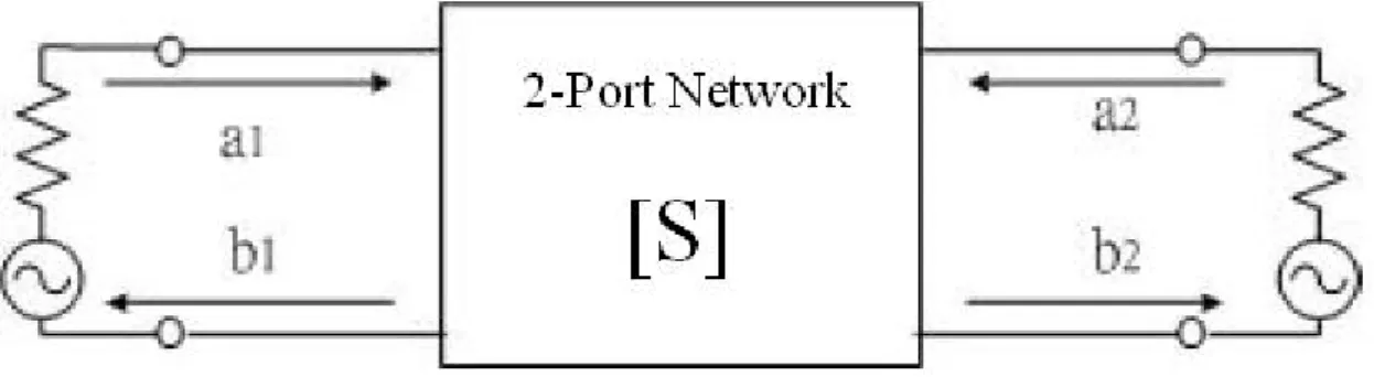
For low frequency, we can use Z-parameters or Y-parameters to represent circuits. But for high frequency, we require S-parameters due to difficulty of open-circuit and short-circuit conditions in measurement. S-parameters are defined by incident waves and reflected waves. For a two-port network, shown in Fig. 2.4, we define the incident wave and the reflected wave for port 1 are a1 and b1. And we define the incident wave
Fig. 2.4 Two-port network
Then we can express the matrix as below.
⎥ ⎦ ⎤ ⎢ ⎣ ⎡ ⎥ ⎦ ⎤ ⎢ ⎣ ⎡ = ⎥ ⎦ ⎤ ⎢ ⎣ ⎡ 2 1 22 21 12 11 2 1 a a S S S S b b
The equation can be written as
b1 =S11a1+S12a2 (2-8) b2 =S21a1+S22a2 (2-9) From equation (2-8) and (2-9), we obtain
0 a 1 1 11 2 a b S = = (2-10) 0 a 1 2 21 2 a b S = = (2-11) 0 a 2 1 12 1 a b S = = (2-12) 0 a 2 2 22 1 a b S = = (2-13)
S11:The reflection coefficient of port 1, when port 2 is matching.
S21:The transmission coefficient from port 1 to port 2, when port 2 is matching.
S12:The transmission coefficient from port 2 to port 1, when port 1 is matching.
S22:The reflection coefficient of port 2, when port 1 is matching.
2.2.2 Stability
When designing amplifiers, stability is always a concern. Amplifiers can be
unstable with certain load and source impedances. We can define some parameters for two-port network [Fig. 2.5].
Fig. 2.5 Two-port network stability parameters
For a two-port network, it is potentially unstable when any port has a negative resistance. It represents Γin >1 or Γout >1.
ΓS <1 (2-14) ΓL <1 (2-15) 1 S -1 S S S L 22 L 21 12 11 in Γ < Γ + = Γ (2-16) 1 S -1 S S S S 11 S 21 12 22 out Γ < Γ + = Γ (2-17) From equation (2-14) ~ (2-17), we can get another form
1 S S 2 S -S -1 K 21 12 2 2 22 2 11 + Δ > = (2-18) Δ =S11S22 -S12S21 <1 (2-19) where K is stability factor. In general, we use equation (2-18) and (2-19) to determine that the circuit is stable or not.
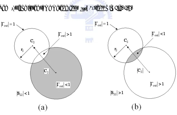
In addition, we can use stability circle to determine the stable region. The stability circle can draw on Smith Chart directly. The output plane is called ΓL-plane, and the
input plane is called ΓS-plane. For ΓL-plane, first, we find the |Γin|=1 circle on Smith
Chart. Second, note the region for |Γin|>1 and |Γin|<1. Finally, we can get the stable
Fig. 2.6 The stable region for ΓL-plane (a) |S11|<1 (b) |S11|>1
The ΓS-plane is the same method for |Γout|=1, shown in Fig. 2.7.
Fig. 2.7 The stable region for ΓS-plane (a) |S22|<1 (b) |S22|>1
2 2 22 21 12 L -S S S r Δ = (2-20)
(
2 2)
22 * * 11 22 L -S S -S C Δ Δ = (2-21) For input stability circle (ΓS-plane), the radius and the center of circle is2 2 11 21 12 S -S S S r Δ = (2-22)
(
2 2)
11 * * 22 11 S -S S -S C Δ Δ = (2-23)2.2.3 Power gain
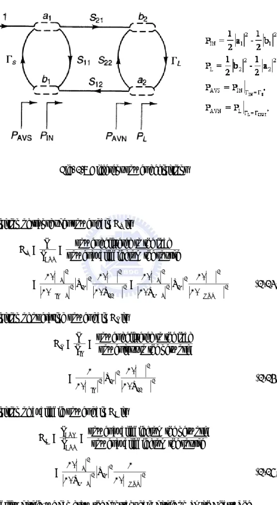
Several power gain equations are used in the design of amplifiers. There are signal flow graph and different powers used in gain equations, shown in Fig. 2.8. The transducer power gain GT, the operating power gain GP, and the available power gain
Fig. 2.8 Different power definitions
The definition of transducer power gain GT is
source the from available power load the to delivered power = P P = G AVS L T 2 L OUT 2 L 2 21 2 S 11 2 S 2 L 22 2 L 2 21 2 S IN 2 S Γ Γ -1 Γ -1 S Γ S -1 Γ -1 = Γ S -1 Γ -1 S Γ Γ -1 Γ -1 = (2-24)
The definition of operating power gain GP is
network the iput to power load the to delivered power = P P = G IN L P 2 L 22 2 L 2 21 2 IN 1-S Γ Γ -1 S Γ -1 1 = (2-25)
The definition of available power gain GA is
source the from available power network the from available power = P P = G AVS AVN A 2 OUT 2 21 2 S 11 2 S Γ -1 1 S Γ S -1 Γ -1 = (2-26)
constant available power gain circle is defined by source reflection coefficient, and the constant operating power gain circle is defined by load reflection coefficient. There is an example for constant available power gain circles, shown in Fig. 2.9.
Fig. 2.9 Constant available power gain circles
2.2.4 Output power and P1dB
In general, we use the dBm as the unit for power, and the definition is
(
)
1(mW) (mW) P log 10 dBm P out out = ⋅ (2-27)For example, 1W is equal to 30dBm. The equation for output power can be written as Pout
(
dBm)
=Pin(
dBm)
+Gain( )
dB (2-28) For ideal case, the gain is the constant, the output power is rising when the input power is rising. But because the non-linear property of active component, the outputpower can not increase infinite. With the increase of the power, the gain will reduce gradually. As input power reaches a certain value, the output power can not increase. So we define a point, when the gain is one dB less than the ideal gain, the point is called 1-dB Compression Point. And the output power at this moment is called P1dB. The 1-dB compression point is used to showing the dynamic range of the circuit. The relation between the input power and the output power is shown in Fig. 2.10.
Fig. 2.10 1-dB compression point
2.2.5 Efficiency
Fig. 2.11 A power amplifier diagram
The efficiency is the conversion ratio from dc power to output power. It plays an important role for power amplifiers. For ideal case, we hope the dc power transform to output power completely. But actuality, it is impossible. There is some power become heat energy. Even if the efficiency is important, we can not increase
unrestrictedly. Because it is trade off between the efficiency and the linearity, we must choose the suitable one.
In general, we define three kinds of efficiency for amplifiers. The first is Drain Efficiency
( )
ηd :DC DC out DC out d I V P P P ⋅ = = η (2-29) The second is Power Added Efficiency
(
ηPAE)
:DC in out PAE P P -P = η (2-30) Finally is Total Efficiency
(
ηtotal)
:in DC out total P P P + = η (2-31) In general cases, ηd >ηPAE >ηtotal. But when the power gain is high, we can drive
total PAE
d η η
η ≈ ≈ .
2.2.6 Distortion
For active components, they have the effects of nonlinearity. For distortion, we can divide into two kinds, one is harmonic distortion, and another one is Intermodulation Distortion.
For harmonic distortion, it says, when a signal enter a nonlinear system, the output generally exhibits frequency components that are integer multiples of the input frequency. If the input is x
( )
t =Acosωt, and the output isy
( )
t x( )
t x( )
t x3( )
t 3 2 2 1 α α α + + ≈ (2-32) theny
( )
t Acos t A cos t A3cos3 t 3 2 2 2 1 ω α ω α ω α + + = (2-33)(
)
(
3cos t cos3 t)
4 A t cos2 1 2 A t Acos 3 3 2 2 1 ω ω α ω α ω α + + + + = (2-34) cos3 t 4 A t cos2 2 A t cos 4 A 3 A 2 A 3 3 2 2 3 3 1 2 2 α α ω α ω α ω α + + ⎟⎟ ⎠ ⎞ ⎜⎜ ⎝ ⎛ + + = (2-35)In equation (2-34), the term with the input frequency is called the fundamental, and the term with high-order is called the harmonics.
enter a nonlinear system, the output will produce some components which are not harmonics, they are called intermodulation (IM). It arises from multiplication of the two signals when their sum is raised to a power greater than unity. We assume the input is x
( )
t =A1cosω1t+A2cosω2t, and the output is just like equation (2-32). Thus,( )
(
)
(
)
2 2 2 1 1 2 2 2 1 11 A cos t A cos t A cos t A cos t
t
y =α ω + ω +α ω + ω
+α3
(
A1cosω1t+A2cosω2t)
3 (2-36) Expanding the left side and discarding dc terms and harmonics, we obtain the following intermodulation products:ω =ω1 ±ω2 :α2A1A2cos
(
ω1 +ω2)
t+α2A1A2cos(
ω1-ω2)
t (2-37)(
)
cos(
2 -)
t 4 A A 3 t 2 cos 4 A A 3 : 2 2 1 2 2 1 3 2 1 2 2 1 3 2 1 ω ω α ω ω α ω ω ± + + = (2-38)(
)
cos(
2 -)
t 4 A A 3 t 2 cos 4 A A 3 : 2 1 2 1 2 2 3 1 2 1 2 2 3 1 2 ω ω α ω ω α ω ω ± + + = (2-39)and these fundamental components
t cos A A 2 3 A 4 3 A : , 2 1 2 1 3 3 1 3 1 1 2 1 ω α α α ω ω ω ⎟ ⎠ ⎞ ⎜ ⎝ ⎛ + + = A A cos t 2 3 A 4 3 A 2 2 1 2 3 3 2 3 2 1 α α ω α ⎟ ⎠ ⎞ ⎜ ⎝ ⎛ + + + (2-40)
What we are interested in are the third-order IM products at 2ω1-ω2 and 2ω2 -ω1, because the third-order IM products are of primary interest since they tend to have frequencies that are within the passband, shown in Fig. 2.12.
Fig. 2.12 IM in a nonlinear system
The key point here is that if the difference between ω and 1 ω is small, 2 2ω1-ω2
and 2ω2 -ω1 will be close to ω and 1 ω . 2
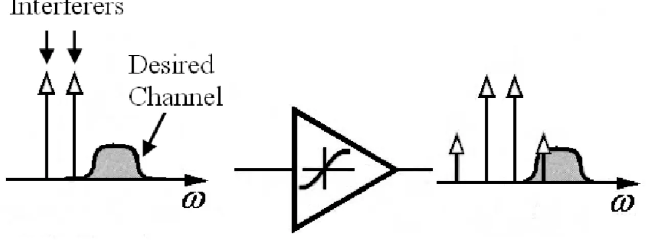
IM is a troublesome effect in RF system. If a weak signal accompanied by two strong interferers experiences third-order nonlinearity, then one of the IM products falls in the interest band, corrupting the desired component, showing in Fig. 2.13.
Fig. 2.13 Corruption of a signal due to IM between two interferers
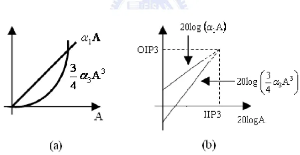
by a two-tone test in which A is chosen to be sufficiently small so that high-order nonlinear terms are negligible and the gain is relatively constant and equal to α1. The
fundamentals increase in proportion to A, and the third-order IM products increase in proportion to A3, shown in Fig. 2.14(a). If plotted on a logarithmic scale, the
magnitude of the IM products grows at three times the rate at which the main components increase. And we define the intersection of the two lines that is the IP3. The horizontal coordinate of the intersection is called the input IP3 (IIP3), and the vertical coordinate is called the output IP3 (OIP3), shown in Fig. 2.14(b).
Fig. 2.14 Growth of output components in an IM test
2.2.7 Adjacent channel power ratio (ACPR)
performance of RF power amplifiers designed for CDMA wireless communication systems, ACPR is a measure of spectral re-growth, appears in the signal sidebands, and is analogous to IM3/IM5 for an analog RF amplifier.
3 or 2 channel offset in the density spectral power 1 channel main in the density spectral power ACPR= (2-41)
There offset frequencies and measurement bandwidths vary with system application.
2.2.8 Peak-to-Average Ratio (PAR)
All single or multi-carrier (modulated or un-modulated) have a peak-to-average ratio. The ratio between the peak power (Pp) and the average power (Pa) of a signal is called the peak-to-average ratio, i.e.
( )
dB Pa Pp 10log , Pa Pp = χ (2-42) The peak-to-average ratio ΔPs of an input signal consisting of N carriers, each having a average power Pi is defined as
∑
∑
= = ⎟ ⎠ ⎞ ⎜ ⎝ ⎛ = Δ n 1 i i 2 n 1 i i i P P Ps χ (2-43)Here χi is the peak-to-average ratio of the ith carrier. If there are n carriers in a given operating bandwidth, it is easy to see that the theoretical maximum
peak-to-average power ratio will be n. Gaussian noise has a peak-to-average ratio of about 9 dB, so very dense multi-carrier systems might require about 6 dB more power
back-off to achieve a similar level of IM distortion compared to a two-carrier signal having the same power.
2.3 Classification of power amplifier
We can determine the class of operation of power amplifiers by the conduction angle, input signal overdrive, and the output load network. The relation between the conduction angle, the input signal over-drive and the power amplifier is shown in Fig. 2.15.
Fig. 2.15 Classification of power amplifier
but class A employ various nonlinear, switching, and wave-shaping techniques. Classes of operation differ not in only the method of operation and efficiency, but also in their power output capability. The power output capability or called transistor utilization factor is defined as output power per transistor normalized for peak drain voltage and current of 1 V and 1 A, respectively.
2.3.1 Class A, B, AB, and C
In class A power amplifier, it is biased so that the output current flows at all the time, and the input signal drive level is kept small enough to avoid driving the
transistor in cut-off. Or we can say that the conduction angle of the transistor is 360°, meaning that the transistor conducts for the full cycle of the input signal.
When the amplifier in class A, it is inherently linear, hence increasing the quiescent current or decreasing the input signal level monotonically decreases IMD and
harmonic levels. Since both positive and negative excursions of the drive affect the drain current, it has the highest gain.
The output power is
out
(
VCEQ -Vmin) (
ICQ-Imin)
21
P = ⋅ (2-44) And in ideal case, Vmin and Imin are both equal to zero. So we can get the maximum
efficiency is 50% I V I V 2 1 P P CC CC CC CC DC max out, max c, = = = η (2-45) The voltage VC reaches the maximum value only if the device is off. Typically the
efficiency is lower than 40% for linear operation. The output power capability is
8 1 I V 2 I 2 V 2 1 I V P P max max max max max max out N = = = (2-46)
In class B power amplifier, the gate bias is set at the threshold of conduction so that the quiescent drain current is zero. And the conduction angle for the transistor is approximately 180°. Thus the transistor conducts only half of the time, either on positive or negative half cycle of the input signal.
Fig. 2.17 The waveform of current We can define that
max CQ fund I 2 I I = = (2-47) π max DC I I = (2-48) out
(
VCEQ -Vmin)
(
Ifund)
2 1
P = (2-49) And in ideal case, Vmin is zero. So we obtain
out,max VCEQIfund 2 1 P = (2-50) 78.5% 4 I V 2 I V 2 1 P P max CC max CC DC max out, max c, = = = = π π η (2-51) 8 1 PN = (2-52) Class B amplifiers are more efficient than class A amplifiers.
In class AB power amplifier, it is a compromise between class A and class B in terms of efficiency and linearity. And it is biased typically to a quiescent point, which is in the region between the cutoff point and the class A bias point. In this case, the
transistor will be turn on for more than a half cycle, but less than a full cycle of the input signal. So the conduction angle in class AB is between 180° and 360°, and the efficiency is between 50 % and 78.5 %.
In class C power amplifier, the gate is biased below threshold so that the transistor is on for less than half of a cycle, or the conduction angle is less than 180 degree. The linearity is lost. The efficiency can achieve toward 100 %, but the output drops down to zero. A typical compromise is a conduction angle of 150° and an ideal efficiency of 85 %. It is little used in solid-state PA because it requires low drain resistances, making implementation of parallel-tuned output filters difficult.
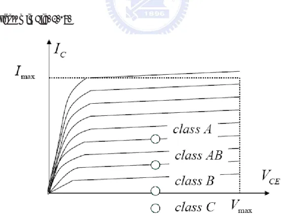
The bias condition for various classes of power amplifier on device I-V characteristics is shown in Fig. 2.18.
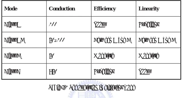
For these classes, transistor works as a transducer and the RF output power is proportional to the RF input power. And the difference is shown in Table 2.1.
Mode Conduction Efficiency Linearity
Class A 100% Poor Excellent
Class AB 50~100% Between A and B Between A and B Class B 50% Moderate Moderate
Class C <50% Excellent Poor Table 2.1 The operation in different mode
The harmonics amplitude is plotted in Fig. 2.19. We can see the odd harmonics be seen to pass through zero at the class B point, but in AB mode, the third harmonic is not negligible.
Fig. 2.19 All components in the current waveform
Then we can plot the efficiency and output power on Fig. 2.20. From this figure the main features of class A, AB, B and C can be determined.
Fig. 2.20 RF power and efficiency with conduction angle
2.3.2 Class D, E, and F
The voltage mode Class D amplifier is defined as a switching circuit that results in the generation of a half-sinusoidal current waveform and a square voltage waveform. The class D power amplifiers use two or more transistors as switches to generate a square drain-voltage waveform. A series-tuned output filter passes only the
fundamental frequency component to the load, the class D amplifiers suffer from a number of problems that make them difficult to realize, especially at high frequencies. The output power is
L 2 DD 2 L 2 L DD L 2 out out R V 2 R R V 2 2 1 R I 2 1 P π π = ⎟ ⎟ ⎟ ⎟ ⎠ ⎞ ⎜ ⎜ ⎜ ⎜ ⎝ ⎛ = = (2-53) And π π 1 R V 2 V P P L DD DD out N = = (2-54)
Class E employs a single transistor operated as a switch. The drain voltage
waveform is the result of the sum of the DC and RF currents charging the drain-shunt capacitance. In optimum class E, the drain voltage drops to zero and has zero slope just as the transistor turns on. The result is an ideal efficiency of 100 %, elimination of the losses associated with charging the drain capacitance in class D, reduction of switching losses, and good tolerance of component variation.
The output power is
L 2 DD L 2 DD 2 out R V 0.577 R V 4 1 2 P ≈ + = π (2-55) And 0.098 R V 1.7 3.6V R V 0.577 I V P P L DD DD L 2 DD max ds, max ds, out N ⋅ ≈ ⋅ = = (2-56)
Class F boosts both efficiency and output by using harmonic resonators in the output network to shape the drain waveforms. The voltage waveform includes one or more odd harmonics and approximates a square wave, while the current includes even
voltage can approximate a half sine wave and the current a square wave. The output power is
[
( )
]
L 2 DD L 2 DD out R V 0.81 2R V 4 P = π ≈ (2-55) And 0.16 2 1 R V 8 2V P I V P P L DD DD out max ds, max ds, out N = ≈ ⋅ = = π π (2-56)For these classes, transistor operates as a switch. And the ideal efficiency is 100 %.
The waveforms of ideal power amplifiers for class A to F are shown in Fig. 2.21.
Chapter 3
Asymmetric LDD MOS Power Cell
3.1 Why asymmetric LDD MOS
In recent research, a new asymmetric-lightly-doped-drain (LDD) MOS transistor that is fully embedded in a CMOS logic without any process modification or extra cost. And it can improve the power performance in radio frequency.
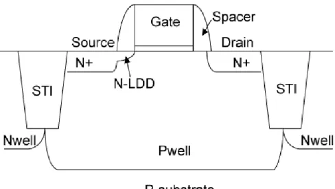
Fig. 3.1 Device structure of asymmetric-LDD MOS
The structure of asymmetric-LDD MOS is shown in Fig. 3.1. The major difference to conventional MOS transistor is no n+-LDD region at drain side. The formed
depletion region under reverse drain bias can sustain large voltage. It can overcome the low breakdown voltage issue for RF power application.
Fig. 3.2 shows the comparison of drain breakdown voltage for conventional and asymmetric-LDD MOS transistors. We can see that the drain breakdown voltage for conventional MOS transistor is about 3.6 V, and the drain breakdown voltage for asymmetric-LDD MOS transistor is about 7.0 V under the same criteria.
Fig. 3.2 The drain breakdown voltage at Vgs=0 V with 0.23μm gate length
This new structure preserves the high frequency operation of sub-μm MOS
transistors with 34 GHz cutoff frequency (ft), it is close to the 35 GHz of conventional
MOS transistor. And the 86 GHz maximum oscillation frequency (fmax) higher than
asymmetric device has larger output power and higher power-added efficiency. The output power is increased by 38 % from 130 to 180 mW/mm at 2.4 GHz, the PAE can be improved by 16 % to conventional device, shown in Fig. 3.3.
Fig. 3.3 Measured RF output power and PAE versus the input power for conventional and asymmetric-LDD MOS transistors at 2.4 GHz.
3.2 Model building
Without n+-LDD region at drain side, the decrease with the gate to drain
capacitance and the gate to source capacitance. In addition, the depletion layer become longer, the resistance from gate to drain become larger.
Fig.3.4.
Fig. 3.4 Asymmetric LDD NMOS model (a) The BSIM model of A-LDD NMOS (b) The equivalent circuit of A-LDD NMOS
Chapter 4
Power Amplifier Design
4.1 Circuit design
In this work, the two-stage circuit has been used to realize a power amplifier. The power amplifier separates into drive stage and power stage. And the drive stage and the power stage operate in class A. The simplified schematic of the circuit is shown in Fig. 4.1.
Fig. 4.1 Schematic of the two stage amplifier circuit
MOS transistor has been used in PA design. The unit cell of asymmetric-LDD MOS transistor designed in this work has 0.18 μm gate-length, 5 μm width, and 10 gate fingers. And asymmetric-LDD MOS transistors have been implemented by foundry standard 0.18μm 1P6M process with only one additional mask but without process modification.
4.2 Design flow
For the design of power amplifier, there are some points that must be considered. Such as supply voltage, frequency range, s-parameters, stability, gain, output power, input power levels, linearity and efficiency. So the first step of design, we have to determine the goal. Then use some methods to reach the goal. When the goal is determined, we choose the operating type and the bias point. Then we use the ideal lumped elements to design the input, internal, and the output matching network with some adjustment. After this, we replace the ideal lumped elements with TSMC model. The design procedure of the amplifier has been carried out through the iteration of ADS and EM simulation. The design flow chart is shown in Fig. 4.2.
4.3 Pre-layout simulation
In this work, the goal we want to reach is shown in Table 4.1.
Operating type Class A
Frequency range 2.4GHz Supply voltage 3V S11 <-10dB Power gain >20dB Output P1dB >24dBm PAE @ P1dB >20% OIP3 >40dBm Table 4.1 The goal of power amplifier
The architecture we use for the power amplifier is just like Fig. 4.1. The transistors in the power amplifier are asymmetric-LDD MOS transistors that introduce in chapter 3. And all of the transistors have 0.18 μm gate-length, 5 μm width, and 10 gate fingers.
For gate bias, the voltage we use in the drive stage and the power stage are both 1 V. And we add inductor to get the result of RF choke and matching.
For drain bias, we use 3 V. And we add inductor to get the result of RF choke and matching.
For stability, we add resistor at gate and inductor at source to improve it. So we can draw the schematic like Fig. 4.3.
Vinput Vload Vs_high Vs_low L L44 R= L=0.2 nH Term Term1 Z=50 Ohm Num=1 I_Probe I_input DC_Bloc k DC_Bloc k3 I_Probe Iload Term Term2 Z=50 Ohm Num=2 DC_Block DC_Block4 L L27 R= L=10 nH L L60 R= L=1.0 nH V_DC SRC3 Vdc=1 V V_DC SRC1 Vdc=3 V asym_50um Q3 V_DC SRC2 Vdc=1.0 V L L26 R= L=10 nH C C48 C=10.0 pF asym_50um Q4 C C47 C=10 pF L L14 R= L=0.1 nH I_Probe Is_low L L57 R= L=1.0 nH R R19 R=50 Ohm I_Probe Is_high C C46 C=10 pF R R20 R=50 Ohm Fig. 4.3 schematic
Then we need to design the matching network. For the input matching network and the inter-stage matching network, we use conjugate matching to get the maximum gain. We use the Smith Chart to design like Fig. 4.4.
Fig. 4.4 Smith Chart for matching network
After matching, we can get the new schematic like Fig.4.5.
Vload Vinput Vs_low Vs_high I_Probe Iload1 Term Term5 Z=50 Ohm Num=5 DC_Block DC_Block6 L L67 R= L=0.2 nH L L78 R=1e-12 Ohm L=2.15 nH C C151 C=1.5 pF C C152 C=2.35 pF L L77 R=1e-12 Ohm L=1 nH R R22 R=50 Ohm R R21 R=50 Ohm L L76 R=1e-12 Ohm L=1 nH I_Probe I_input1 P_1Tone PORT2 Freq=RFfreq P=dbmtow(Pavs) Z=Z_s Num=2 DC_Block DC_Block5 C C150 C=5.7096 pF L L75 R=1e-12 Ohm L=2.2 nH I_Probe Is_low1 C C149 C=10 pF asy m_50um Q12 asym_50um Q11 asy m_50um Q10 asym_50um Q9 C C148 C=10.0 pF L L74 R= L=10 nH V_DC SRC6 Vdc=1.0 V L L73 R= L=10 nH asym_50um Q8 C C147 C=10 pF I_Probe Is_high1 V_DC SRC5 Vdc=3 V L L69 R= L=0.1 nH V_DC SRC4 Vdc=1 V
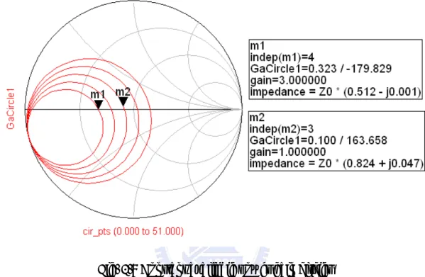
Then we need to design the output matching network. For a power amplifier, the power is very important. So we must design the output matching network to get the maximum power. Here we use the load-pull method in ADS to design. Load-pull is a method that can find out the impedance of the best power and the best efficiency in Smith Chart, shown in Fig. 4.6 and Fig. 4.7.
Fig. 4.7 Simulation result of load-pull in ADS The simulation result of load-pull in this work is shown in Fig. 4.8.
indep(PAE_contours_p) (0.000 to 45.000) PA E_ co nt ou rs _p m1 indep(Pdel_contours_p) (0.000 to 39.000) P del_c ont our s_p m2 m1 indep(m1)= PAE_contours_p=0.529 / 172.854 level=27.463902, number=1 impedance = Z0 * (0.309 + j0.056) 2 m2indep(m2)= Pdel_contours_p=0.700 / -172.535 level=26.730701, number=1 impedance = Z0 * (0.177 - j0.063) 4 m2 indep(m2)= Pdel_contours_p=0.700 / -172.535 level=26.730701, number=1 impedance = Z0 * (0.177 - j0.063) 4 m1 indep(m1)= PAE_contours_p=0.529 / 172.854 level=27.463902, number=1 impedance = Z0 * (0.309 + j0.056) 2
We can get the impedance for power (blue) and efficiency (red) from Fig. 4.8. We select the point near these two centers of a circle, accord with the goals of power and efficiency at the same time.
After repeated matching, we get the power amplifier with ideal lumped elements. Then we replace the ideal lumped elements with TSMC model. And after tuning, we get the final power amplifier. The schematic is shown as follow.
Vload Vinput Vs_high Vs_low I_Probe Iload Term Term2 Z=50 Ohm Num=2 DC_Block DC_Block4 C C98 C=3.3 pF L L61 R=1e-12 Ohm L=1.4 nH C C100 C=2.35 pF C C99 C=1.5 pF L L62 R=1e-12 Ohm L=2.15 nH R R20 R=50 Ohm L L66 R= L=1.0 nH R R19 R=50 Ohm I_Probe I_input P_1Tone PORT1 Freq=RFfreq P=dbmtow(Pavs) Z=Z_s Num=1 DC_Block DC_Block3 L L64 R=1e-12 Ohm L=2.2 nH C C129 C=5.7096 pF L L65 R= L=1.0 nH V_DC SRC3 Vdc=1 V L L44 R= L=0.2 nH L L14 R= L=0.1 nH V_DC SRC1 Vdc=3 V I_Probe Is_high C C46 C=10 pF asy m_50um Q3 L L27 R= L=10 nH V_DC SRC2 Vdc=1.0 V L L26 R= L=10 nH C C48 C=10.0 pF asym_50um Q7 asym_50um Q6 asy m_50um Q5 asym_50um Q4 C C47 C=10 pF I_Probe Is _low
Vinput Vload Vs_high Vs_low TSMC018RF_MIMCAP C115 Cs=951.6 fF wt=30 um lt=30 um Type=MiM with shield TSMC018RF_MIMCAP
C116 Cs=951.6 fF wt=30 um lt=30 um Type=MiM with shield TSMC018RF_MIMCAP
C117 Cs=951.6 fF wt=30 um lt=30 um Type=MiM with shield TSMC018RF_MIMCAP
C118 Cs=472.4 fF wt=21 um lt=21 um Type=MiM with shield TSMC018RF_MIMCAP
C120 Cs=588.6 fF wt=23 um lt=24 um Type=MiM with shield TSMC018RF_MIMCAP
C121 Cs=588.6 fF wt=23 um lt=24 um Type=MiM with shield
TSMC018RF_MIMCAP
C122 Cs=588.6 fF wt=23 um lt=24 um Type=MiM with shield TSMC018RF_MIMCAP
C126 Cs=588.6 fF wt=23 um lt=24 um Type=MiM with shield L L58 R=1e-12 Ohm L=2.15 nH TSMC018RF_MIMCAP C123 Cs=745.3 fF wt=26 um lt=27 um Type=MiM with shield TSMC018RF_MIMCAP
C105 Cs=745.3 fF wt=26 um lt=27 um Type=MiM with shield TSMC018RF_MIMCAP
C112 Cs=951.6 fF wt=30 um lt=30 um Type=MiM with shield TSMC018RF_MIMCAP
C111 Cs=951.6 fF wt=30 um lt=30 um Type=MiM with shield TSMC018RF_MIMCAP
C113 Cs=951.6 fF wt=30 um lt=30 um Type=MiM with shield
TSMC018RF_MIMCAP
C124 Cs=951.6 fF wt=30 um lt=30 um Type=MiM with shield TSMC018RF_MIMCAP
C128 Cs=951.6 fF wt=30 um lt=30 um Type=MiM with shield TSMC018RF_MIMCAP
C127 Cs=951.6 fF wt=30 um lt=30 um Type=MiM with shield L L60 R=1e-12 Ohm L=2.2 nH DC_Block DC_Block3 P_1Tone PORT1 Freq=RFfreq P=dbmtow(Pavs) Z=Z_s Num=1 I_Probe I_input I_Probe Iload Term Term2 Z=50 Ohm Num=2 DC_Block DC_Block4 L L59 R=1e-12 Ohm L=1.35 nH V_DC SRC3 Vdc=1 V L L44 R= L=0.2 nH L L14 R= L=0.1 nH TSMC_CM018RF_RES_RF R17 R=50.72 Ohm l=13.001 um w=2 um
Type=P+ Poly w/i silicide (0.18<=w<=5.0)(RF)
V_DC SRC1 Vdc=3 V I_Probe Is_high C C46 C=10 pF asym_50um Q3 TSMC_CM018RF_INDS2_STD L54 lay=6 rad=30 um nr=0.5 w=6 um TSMC_CM018RF_INDS2_STD L55 lay=6 rad=30 um nr=0.5 w=6 um TSMC_CM018RF_INDS2_STD L49 lay=6 rad=30 um nr=2.5 w=6 um L L27 R= L=10 nH V_DC SRC2 Vdc=1.0 V L L26 R= L=10 nH TSMC_CM018RF_RES_RF R18 R=50.72 Ohm l=13 um w=2 um
Type=P+ Poly w/i silicide (0.18<=w<=5.0)(RF) C C48 C=10.0 pF asym_50um Q7 asym_50um Q6 asym_50um Q5 asym_50um Q4 C C47 C=10 pF I_Probe Is_low
Fig. 4.10 TSMC model schematic
The simulation results are shown as follow.
2 4 6 8 0 10 -20 -15 -10 -5 -25 0 -150 -100 -50 0 -200 50 freq, GHz dB (S (2 ,1 )) m19 dB (S (1 ,1 )) m17 dB (S (2 ,2 )) m18 m19 freq= dB(S(2,1))=25.7882.400GHz m17 freq= dB(S(1,1))=-13.5282.400GHz m18 freq= dB(S(2,2))=-6.5542.400GHz
2 4 6 8 0 10 0.833 1.667 2.500 3.333 4.167 0.000 5.000 freq, GHz Mu 1 m5 Mu P rime 1 m12 St abFac t1 m9 m5 freq= Mu1=1.000 Min 100.0MHz m12freq= MuPrime1=1.000 Min 100.0MHz m9freq= StabFact1=1.973 Min 2.200GHz
Fig. 4.12 Stability factor of pre-layout simulation
-15 -10 -5 0 5 10 15 -20 20 10 15 20 25 5 30 Pin Ga in m14 m15 m14 indep(m14)= plot_vs(Gain, Pin)=25.767-20.000 m15 indep(m15)= plot_vs(Gain, Pin)=24.7311.500
-15 -10 -5 0 5 10 15 -20 20 10 15 20 25 5 30 Pin P out m10 m10 indep(m10)= plot_vs(Pout, Pin)=26.2311.500
Fig. 4.14 Output power of pre-layout simulation
-15 -10 -5 0 5 10 15 -20 20 10 20 30 40 50 0 60 Pin PAE
m16
m16
indep(m16)=
plot_vs(PAE, Pin)=23.246
1.500
-15 -10 -5 0 5 10 15 -20 20 -60 -40 -20 0 20 -80 40 Pin S pec tr um [1] S pec tr um [3]
Fig. 4.16 IP3 of pre-layout simulation
The layout has to be modified after post layout simulation.
4.4 Post-layout simulation
The critical DC power line generates parasitic resistance. To prevent loss, the line has to be widened. After modify the layout simulate the circuit again and find the best layout topology.
Fig. 4.18 Post-layout simulation with line calculation
Modify the layout with better simulation result. Then determinate the best layout topology and tape out. With the simulation, the final layout is shown in Fig.4.19.
Fig. 4.19 The layout after post-layout simulation
2 4 6 8 0 10 -40 -30 -20 -10 -50 0 -100 -50 0 -150 50 freq, GHz dB (S (2 ,1 )) m19 dB (S (1 ,1 )) m17 dB (S (2 ,2 )) m18 m19 freq= dB(S(2,1))=26.5862.400GHz m17 freq= dB(S(1,1))=-16.4972.400GHz m18 freq= dB(S(2,2))=-8.8812.400GHz
Fig. 4.20 S-parameter of post-layout simulation
2 4 6 8 0 10 0.833 1.667 2.500 3.333 4.167 0.000 5.000 freq, GHz Mu 1 m5 Mu Pr im e 1 m12 St a b F a ct 1 m9 m5 freq= Mu1=1.000 Min 100.0MHz m12freq= MuPrime1=1.000 Min 100.0MHz m9freq= StabFact1=1.570 Min 2.090GHz
-15 -10 -5 0 5 10 15 -20 20 10 15 20 25 5 30 Pin Ga in m14 m15 m14 indep(m14)= plot_vs(Gain, Pin)=26.559-20.000 m15 indep(m15)= plot_vs(Gain, Pin)=25.474-0.500
Fig. 4.22 Power gain of post-layout simulation
-15 -10 -5 0 5 10 15 -20 20 10 15 20 25 5 30 Pin P out
m10
m10
indep(m10)=
plot_vs(Pout, Pin)=24.974
-0.500
-15 -10 -5 0 5 10 15 -20 20 10 20 30 40 50 0 60 Pin PAE
m16
m16
indep(m16)=
plot_vs(PAE, Pin)=20.032
-0.500
Fig. 4.24 Power Added Efficiency of post-layout simulation
-15 -10 -5 0 5 10 15 -20 20 -60 -40 -20 0 20 -80 40 Pin S pec tr um [1] S pec tr um [3]
Summary of post-layout simulation is shown in Table 4.2. S11 -16.5dB Power gain 26.5dB Output P1dB 24.9dBm PAE @ P1dB 20% OIP3 >40dBm Table 4.2 The result of power amplifier
From Table 4.2, we can see the result is up to specification.
4.5 Measurement
For this work, the inductor of matching network is off chip. But there are some mistakes on design, so the chip is not work. The photograph of the chip is shown in Fig. 4.26.
Chapter 5
Conclusion
We have designed an asymmetric-LDD MOS transistor which has twice drain breakdown voltage to the conventional one. Besides, the power amplifier has been designed by single ended and fabricated by TSMC 0.18μm 1P6M process without any process modification.
According to simulation, this power amplifier can achieve 26.5dB power gain, 24.9dBm output P1dB, and 20% PAE at P1dB.
This research demonstrated that the asymmetric-LDD MOS transistor successfully implemented on a CMOS power amplifier with wonderful performance. This design method has great opportunity to be future trend.
Reference
[1] M.C. King, T. Chang, A. Chin, “RF power performance of asymmetric-LDD MOS transistor for RF-CMOS SOC design”, IEEE Microwave and Wireless Components Letters, vol. 17, no. 6, pp. 445–447, June 2007.
[2] J.F. Chen, J. Tao, P. Fang, C. Hu, “0.35- m asymmetric and symmetric LDD device comparison using a reliability/speed/power methodology”, IEEE Electron Device Letters, vol. 19, no. 7, pp. 216-218, July 1998.
[3] A. Litwin, O. Bengtsson, J. Olsson, “Novel BiCMOS compatible, short channel LDMOS technology for medium voltage RF & power applications”, IEEE Symp, pp. 289-292, 2002.
[4] J.C. Guo, C.H. Huang, K.T. Chan, W.Y. Lien, C.M. Wu, Y.C. Sun, “0.13μm low voltage logic base RF CMOS technology with 115GHz ft and 80GHz fmax”, 33rd European Microwave Conference, pp. 682-686, 2003.
[5] G. Miller Managing, “TSMC announces 0.18-micron mixed signal and RF CMOS processes”, RF Globalnet
[6] K.-E. Ehwald, B. Heinemann, W. Roepke, W. Winkler, H. Rücker, F. Fuernhammer, D. Knoll, R. Barth, B. Hunger, H. E. Wulf, R. Pazirandeh, N. Ilkov, “High performance RF LDMOS transistors with 5nm gate oxide in a 0.25m SiGe:C BiCMOS technology”, IEDM Tech. Dig., pp. 40.4.1-40.4.4, 2001.
[7] C.-C. Yen, H.-R. Chuang, “A 0.25-µm 20-dBm 2.4-GHz CMOS power amplifier with an Integrated diode linearizer”, IEEE Microwave & Wireless Components Letter, vol. 13, no. 2, pp. 45-47, 2003.
[8] V. Knopik, B. Martineau, D. Belot, “20 dBm CMOS class AB power amplifier design for low cost 2GHz-2.45GHz consumer applications in a 0.13μm technology”, Proc. IEEE Int. Symp. Circuits and Systems, Kobe, Japan, vol. 3, pp. 2675-2678, May 2005. [9] C. Lu, A.-V. H. Pham, M. Shaw, C. Saint, “Linearization of CMOS broadband power
amplifiers through combined multi-gated transistors and capacitance compensation”, IEEE Transaction on Microwave Theory and Techniques, pp. 2320-2328, November 2007.
[10] Y. Eo, K. Lee, “A 2.4GHz/5.2GHz CMOS power amplifier for dual-band applications”, IEEE MTT-S Int. Microwave Symp. Dig, Fort Worth, TX, vol. 3, pp. 1539-1542, June 2004.
[11] P. Haldi, D. Chowdhury, G. Liu, A. M. Niknejad , “A 5.8GHz linear power amplifier in a standard 90nm CMOS process using a 1V power supply”, IEEE Radio Frequency Integrated Circuits Symp, pp. 431-434, 2007.
[12] Y. Eo, K. Lee, “High efficiency 5GHz CMOS power amplifier with adaptive bias control circuit”, IEEE RFIC Symp. Dig, Fort Worth, TX, pp. 575-578, June 2004.
[13] E. Chen, D. Heo, M. Hamai, J. Laskar, D. Bien, “0.24-um CMOS technology for bluetooth power applications”, Proc. IEEE Radio and Wireless Conference, pp. 163-166, 2000.
[14] G. Krieger, R. Sikora, P. Cuevas, M. Misheloff, “Moderately doped NMOS
(M-LDD)—hot electron and current drive optimization”, IEEE Trans. Electron Devices, vol. 38, pp. 121, January 1991.
[15] T.H. Lee, H. Samawati, H.R. Rategh, “5-GHz CMOS wireless LANs”, IEEE Transaction Microwave Theory and Technique, vol. 50, pp. 268-280, 2002. [16] T. Sowlati, D. Leenaerts, “A 2.4GHz 0.18um CMOS self-biased cascode power
amplifier with 23dBm output power”, ISSCC Advanced RF Techniques, session 17, February 2002.
[17] Thomas H. Lee, The design of CMOS radio-frequency integrated circuit, Cambridge University Press, 2000.
[18] D.M. Pozar, Microwave engineering, Addison-Wesley, 1990. [19] Behzad Razavi, RF microelectronics, Prentice-Hall, Inc., 1998.
[20] S.C. Cripps, RF power amplifiers for wireless communications, Norwood, MA: Artech House, 1999.