Spin-dependent Hall effect in semiconductor quantum wells
H. C. Huang, O. Voskoboynikov, and C. P. LeeCitation: Journal of Applied Physics 95, 1918 (2004); doi: 10.1063/1.1641147
View online: http://dx.doi.org/10.1063/1.1641147
View Table of Contents: http://scitation.aip.org/content/aip/journal/jap/95/4?ver=pdfcov
Published by the AIP Publishing
Articles you may be interested in
Degeneracy and effective mass in the valence band of two-dimensional (100)-GaAs quantum well systems
Appl. Phys. Lett. 104, 092102 (2014); 10.1063/1.4867086
Temperature dependence of the bandwidth of delocalized states for n-InGaAs/GaAs in the quantum Hall effect regime
Low Temp. Phys. 39, 50 (2013); 10.1063/1.4775752
Fabrication of samples for scanning probe experiments on quantum spin Hall effect in HgTe quantum wells
J. Appl. Phys. 112, 103713 (2012); 10.1063/1.4767362
Gate voltage dependence of nuclear spin relaxation in an impurity-doped semiconductor quantum well
Appl. Phys. Lett. 96, 071907 (2010); 10.1063/1.3309687
Spin Effects in the nIn x Ga1x As/GaAs Double Quantum Well Magnetoresistance Under Tilted Magnetic Fields
AIP Conf. Proc. 893, 631 (2007); 10.1063/1.2730049
Spin-dependent Hall effect in semiconductor quantum wells
H. C. Huang, O. Voskoboynikov,a)and C. P. LeeNational Chiao Tung University, 1001 Ta Hsueh Rd., Hsinchu, 300, Taiwan, Republic of China
共Received 21 July 2003; accepted 21 November 2003兲
We present a theoretical study of the spin-dependent scattering of electrons from screened attractive and repulsive impurities in III-V semiconductor quantum wells. The effective one-band Hamiltonian and the Rashba spin–orbit interaction are used. We demonstrated that the asymmetry of the spin-dependent skew-scattering and side-jump effect can lead to a quite large spin-dependent 共anomalous兲 Hall effect at zero magnetic field in all-semiconductor quantum well structures. Our theory predicts a measurable spin-dependent Hall angle that reaches about 2.5⫻10⫺3rad for a CdTe/InSb/CdTe quantum well with impurities doped in the center of the well. © 2004 American
Institute of Physics. 关DOI: 10.1063/1.1641147兴
I. INTRODUCTION
The extra degree of freedom provided by the electron spin may open up further enhancements for semiconductor devices. The spin-transistor proposed by Datta and Das1is an example of a spin-controlled device based on semiconductor two-dimensional共2-D兲 channels. For this reason, theoretical studies of spin-dependent electron processes in 2-D semicon-ductor structures have attracted a lot of interest since a par-ticular branch of semiconductor electronics 共so-called spin-tronics兲 has become a focus of study.2– 4
Recently, detection of the electron polarization in para-magnetic metals5,6 and semiconductors7 through the spin-dependent Hall effect 共SDHE兲 has been proposed. This is quite similar to the exploitation of the anomalous Hall effect 共AHE兲, which can be observed in magnetic metals or semi-conductors without external magnetic field共see, for instance Ref. 8, and references therein兲. The key point of the expla-nation of those effects is the presence of the spin–orbit in-teraction 共SOI兲. Considerable work on the AHE has been done in the last 50 years since the pioneering work of Kar-plus and Luttinger.9 It is generally recognized that two mechanisms contribute to the AHE. Those are the side-jump effect共SJ兲 proposed by Karplus and Luttinger9and Berger,10 and the skew-scattering共SS兲 proposed by Smit.11It is com-monly believed that the first mechanism can be more signifi-cant in metal alloys or semiconductors with relatively large resistivity, while the second one prevails in systems with low resistivity.
In the absence of magnetic impurities and at low tem-peratures, the main source of the spin-dependent scattering processes is the SO coupling to local defects. The effect of the SOI on the electron transport and relaxation in 2-D semi-conductor systems has been studied for a long time.12–15We recently investigated the spin-dependent scattering processes in the bulk of nonmagnetic semiconductors in the presence of the SOI.16 In semiconductor quantum wells 共QWs兲 the effect of the SOI on the processes of scattering becomes even more stronger that in the bulk. This is a result of the
local-ization of electrons’ wave functions in the conduction channel.17,18
In this article, we present a model of the spin-dependent electron scattering from impurities located in the center QWs of nonmagnetic III-V semiconductors. We calculate contribu-tions from the SS and SJ mechanisms to the SDHE. Our calculation is based on the effective-one-band Hamiltonian19,20 and Rashba-type model of the SOI.12,21,22 For QWs of narrow-gap semiconductors共systems with large SO coupling parameters兲 and with impurities located in the center of the wells, we obtained relatively large spin-dependent Hall angles 共SOHAs兲.
The article is organized as follows. Section II describes the method we use to calculate the spin-dependent 共Mott兲 cross section for 2-D electrons scattered from impurities in semiconductor QWs. Section III presents the method of cal-culation of the off-diagonal element of the conductivity ten-sor in QWs with account of the Mott scattering. The calcu-lation results are presented in Sec. IV and conclusions are given in Sec. V.
II. BASIC EQUATIONS AND DESCRIPTION OF THE SPIN-DEPENDENT SCATTERING
We consider III-V semiconductor QWs with charged im-purities and use the approximate one-electron-band effective Hamiltonian in the following form:19,20
Hˆ ⫽Hˆ0⫹Vˆim共r兲, 共1兲
where H0 is the Hamiltonian of the system without impuri-ties: Hˆ0⫽⫺ ប2 2 “r
冋
1 m共E,r兲册
“r⫹V共r兲.Vˆim(r) is the impurity potential, “r stands for the spatial gradient, m(E,r) is the energy, and position-dependent elec-tron effective mass is
a兲Electronic mail: [email protected]
1918
0021-8979/2004/95(4)/1918/6/$22.00 © 2004 American Institute of Physics
1 m共E,r兲⫽ 2 P2 3ប2
冋
2 E⫹Eg共r兲⫺V共r兲 ⫹ 1 E⫹Eg共r兲⫹⌬共r兲⫺V共r兲册
,where E is the electron energy, V(r) is the confinement po-tential of the well, Eg(r) and ⌬共r兲 stand for the
position-dependent band gap and the SO splitting in the valence band, respectively, and P is the momentum matrix element.
The impurity potential consists of two parts, Vˆim共r兲⫽Vc共r兲⫹Vso共r兲,
where Vc(r) is the Coulomb potential of the charged
impu-rity and Vso(r) describes the SO coupling with the impurity
Vso共r兲⫽i␣共E,r兲“Vc共r兲•关ˆ⫻“r兴, where12,18,21,22 ␣共E,r兲⫽P 2 3
冋
1 关E⫹Eg共r兲⫺V共r兲兴2 ⫺ 1 关E⫹Eg共r兲⫹⌬共r兲⫺V共r兲兴2册
. 共2兲We describe symmetrical QWs of thickness L and denote by z the direction perpendicular to the well interfaces. For sys-tems with sharp discontinuity in the conduction band edge between the QW共material 1兲 and the barrier region 共material 2兲, the confinement potential can be presented as
V共r兲⫽
再
0, ⫺L/2⭐z⭐L/2;共r苸1兲 V0, 兩z兩⬎L/2;共r苸2兲
. 共3兲
We assume that an isolated impurity is located in the center of the wells (z⫽0), and the unscreened Coulomb potential of the impurity is given as
Vc0共r兲⫽⫺ Ze
2
4⑀s关2⫹z2兴1/2, 共4兲
where ⫽(x,y) is the position vector parallel to the inter-faces, ⑀s⫽(⑀1⫹⑀2)/2 is the average permittivity of the
sys-tem, Z is the charge of the impurity, and e is the electron charge. For most III-V semiconductor QWs, we can neglect the image potential, and we assume that for simplicity.
The Rashba term in Hˆ0does not occur due to the
reflec-tion symmetry of the quantum well.21,22Considering only the electrons’ elastic scattering within the first subband of the well, we present the solution of the confinement problem with the Hamiltonian Hˆ0 as19,23
⌿共,z兲⫽s共兲
1共z兲, 共5兲
where 1(z) is the normalized electron wave function in z
direction, and s⫽⫾1 is the quantum number related to the spin states. The eigen-energy Enz in z direction can be
ob-tained easily from the well-known Ben–Daniel–Duke boundary conditions.20,21
By taking the average
V ˜ 共兲⫽
冕
⫺⬁ ⫹⬁
dz1*共z兲Vim共r兲1共z兲,
and following the approach described in Refs. 19, 23 and 24, we obtain statistically screened and averaged quasi-2-D scat-tering potential in the following form:
V ˜ c共兲⫽⫺ ប2Ze2 aB*m1共0兲
冕
0 ⬁ dq ⑀共q兲J0共q兲 ⫻冕
⫺⬁ ⫹⬁ dz兩1共z兲兩2e⫺q兩z兩, V ˜ so共兲⫽i ប2Ze2 aB*m1共0兲冕
0 ⬁qdq ⑀共q兲J1共q兲 •冋
␣1共E兲冕
z⭐兩L/2兩 dz兩1共z兲兩2e⫺q兩z兩 ⫹␣2共E兲冕
z⭓兩L/2兩 dz兩1共z兲兩2e⫺q兩z兩册
⫻ s , where aB*⫽⑀sប2/e2m1(0) is the effective Bohr radius in the
well, Jn(x) is the Bessel function, ⑀共q兲⫽1⫹qf
q
is the 2-D dielectric function,
qf⫽ 1 aB* m1共Ef兲 m1共0兲
再
1⫹ d dEln关m1共E兲兴兩EF冎
is the 2-D Thomas–Fermi screening constant, EF is the
Fermi energy of the system,24and
E⫽E⫹E1z.
Due to the radial symmetry of the potentials V˜c() and
V ˜
so(), we can present the wave functions() as the
fol-lowing:
s共兲⫽
兺
l⫽⫺⬁ l⫽⫹⬁Rls共兲eils.
where l is the orbital momentum number ands is the spin function upon which the Pauli matrix vector operates.
The quasi-2-D Schro¨dinger equation for the radial wave function is given by
再
ប2 2m˜共E兲冋
1 d d冉
d d冊
⫺ l2 2⫹k 2册
⫺V˜ c共兲⫹lV˜so共兲冎
Rl s共兲 ⫽0, 共6兲 where k⫽1 ប冑
2m˜共E兲Eis the wave vector of the 2-D electrons, and
1919 J. Appl. Phys., Vol. 95, No. 4, 15 February 2004 Huang, Voskoboynikov, and Lee
1 m˜共E兲⫽ 1 m1共E兲
冕
z⭐兩L/2兩 dz兩1共z兲兩2 ⫹m1 2共E兲冕
z⭓兩L/2兩 dz兩1共z兲兩2.At a large distance from the scattering center, the asymptotic of the radial function is given by
Rls共兲→Als关cos␦lsJl共k兲⫺sin␦lsNl共k兲兴; →⬁, where␦ls is the scattering phase shift25,26and Nl is the
Neu-mann function. To solve the scattering problem we use the variable phase approach,26,27 which assumes that the phase function␦ls() at the pointdetermines the phase shift pro-duced by the part of the potential contained within the cycle of a radius. The scattering phase shift for the total potential is equal to the asymptotic value
␦ls⫽ lim →⬁␦l
s共兲.
The phase function␦ls() satisfies the following differential equation: d␦l s共兲 d ⫽⫺ 2m˜共E兲 ប2 关V˜c共兲⫺lV˜so共兲兴 ⫻关cos␦ls共兲J l共k兲⫺sin␦l s共兲N l共k兲兴2, 共7兲
with the boundary condition
␦ls共0兲⫽0. 共8兲
The complex 2-D scattering amplitude we present as25,28
Fs共E,兲⫽关 f 共E,兲⫹zg共E,兲兴s, 共9兲
where fs() and g() describe scattering without and with electron spin reorientation, respectively, and they are deter-mined by the following:28
f共E,兲⫽
兺
l⫽0 ⬁ flcos共l兲, 共10兲 g共E,兲⫽兺
l⭓1 ⬁ glsin共l兲, 共11兲 where fl⫽冑
1 2k再
exp共2i␦0兲⫺1, l⫽0exp共i2␦l⫹兲⫹exp共i2␦l⫺兲⫺2, l⭓1,
gl⫽i
冑
1
2k关exp共i2␦l⫹兲⫺exp共i2␦l⫺兲兴,
is the scattering angle between initial (ki) and final (kf)
wave vectors. When electrons are spin polarized parallel to the z axis, the Mott scattering cross section29 can be ex-pressed in terms of the incident electron spin-polarization P as the following:
共E,兲⫽I共E,兲⫹G共E,兲P, 共12兲
where I() is the differential cross section for the unpolar-ized incident electrons共the symmetric scattering part兲
I共E,兲⫽兩 f 共E,兲兩2⫹兩g共E,兲兩2, and
G共E,兲⫽ f*共E,兲g共E,兲⫹ f 共E,兲g*共E,兲, 共13兲
is the spin-flip part of the scattering cross section共the asym-metric scattering part兲.
III. SPIN-DEPENDENT HALL EFFECT IN 2-D CHANNELS
In the Pauli approach to the explanation of the origin of the AHE,8 the total electron velocity is presented as
vks⫽1
ប “kE共k兲⫹wk
s 共14兲
where E(k) is the dispersion relation of 2-D electrons in the well, and wks is the anomalous velocity, which can be written in the following form:8,21,22
wks⫽␣关sÃk兴
im
, 共15兲
whereimis the electron momentum relaxation time resulted
from impurity scattering, and s is the unit vector parallel to the spin polarization.
The total electron current can be obtained by averaging the total velocity over the electron distribution function fs(k). In the linear approximation with respect to the
exter-nal electric field F,30–32this leads to
J⫽⫺兩e兩
兺
k,s
vksfs共k兲⫽J0⫹Js⫽cF⫹c s关sÃF兴
s , 共16兲
wherecis the diagonal element of the conductivity tensor
andcs is the spin-dependent Hall conductivity共off-diagonal element of the conductivity tensor兲. If the concentration of scatterers is low, one can assume these impurities scatter the electrons independently. In this approximation, the Boltz-mann transport equation for the electron distribution function fs(k) is given by ⫺兩e兩ប F“kfs共k兲⫽
兺
k,s W0共k,k˜兲⫹Ws共k,k˜兲 ⫻关 fs共k兲⫺ fs共k˜兲兴, 共17兲 where W0共k,k˜兲⫽ 8ប3Am˜2共E兲kI共k,k˜兲Nim␦关E共k兲⫺E共k˜兲兴, 共18兲
Ws共k,k˜兲⫽
8ប3
Am˜2共E兲k PG共k,k˜兲Nim␦关E共k兲⫺E共k˜兲兴,
共19兲 I共k,k˜兲⫽I关E共k兲,兴, G共k,k˜兲⫽G关E共k兲,兴, 共20兲
P⫽1
ns⫽⫾1
兺
sns, n⫽n⫹1⫹n⫺1, 共21兲
where W0(k,k˜) and Ws(k,k˜) are the scattering transition
probabilities per unit time due to symmetric and asymmetric [This article is copyrighted as indicated in the article. Reuse of AIP content is subject to the terms at: http://scitation.aip.org/termsconditions. Downloaded to ] IP:
scattering, respectively, Nim is the impurity concentration, P
is the polarization of the 2-D electronic gas, ns is the
con-centration of the s-polarized electrons in the 2-D channel, and A is the system area. In the linear approximation, the electron distribution function can be written in the form
fs共k兲⬇ f0共E兲⫹P0共E兲共k"F兲⫹Ps共E兲共k•关sÃF兴兲. 共22兲
Substituting fs(k) into the Boltzmann equation, we obtain
the coefficients P0(E) and Ps(E), and then the components
of the conductivity tensor.
Finally, the off-diagonal element of the conductivity ten-sor obtained from Eq. 共16兲 consists of two parts,
cs⫽ SS s ⫹
SJ
s 共23兲
where SSs is the contribution from the skew-scattering 共which comes from the spin-dependent part of the elastic scattering兲 and SJs is the side-jump contribution 共which comes with the anomalous velocity兲. For the case of the de-generated electronic system 共low-temperature limit兲, those two contributions can be presented as the following:
SS s ⫽បe 2N im 2 s⫽⫾1
兺
s冉
im s m ˜s冊
2 G˜s共kF s兲3, 共24兲 SJ s ⫽⫺ e 2 4បs⫽⫾1兺
s␣s共kFs兲2. 共25兲 In Eqs.共24兲 and 共25兲, G˜s⫽冕
0 2 G共EF s ,兲关1⫺cos共兲兴sin共兲d, 共26兲 1 im s ⫽ 2បNim m ˜s kF s Is g, 共27兲 I ˜ s⫽冕
0 2 I共EFs,兲关1⫺cos共兲兴d, 共28兲 m˜s⫽m˜ (EF s), ␣s⫽␣(E Fs), and the Fermi energy E F s for the
s-group of the polarized electrons is the solution of the fol-lowing equation: EFs⫽ ប 2 2m˜s共kF s兲2⫹E 1z, 共29兲
with the electron Fermi wave vector defined as the follow-ing:
kFs⫽关2n共1⫹sP兲兴1/2. 共30兲
The tangent of the spin-dependent Hall angle共SDHA兲 is the sum of two tangents, and can be presented as
tan共H兲⫽tan共H SS兲⫹tan共 H SJ兲, 共31兲 where tan共HSS兲⫽SS s , tan共H SJ兲⫽SJ s , 共32兲 and c⫽e 2k F s2 4m˜ im s 兩 P⫽0. 共33兲
IV. CALCULATION RESULTS
To demonstrate the actual value of the SDHE in semi-conductor QWs, we first present results of our simulations for Al0.48In0.52As/In0.53Ga0.47As/Al0.48In0.52As 共IGA兲
sym-metrical QWs, which possessed the well-developed growth technology. The parameters taken in this calculation are the following: Eg1⫽0.813 eV, Eg2⫽1.508 eV, ⌬1⫽0.361 eV,
⌬2⫽0.332 eV, m1(0)⫽0.041m0, m2(0)⫽0.075m0, ⑀1
⫽14, ⑀2⫽12.5, and V0⫽0.504 eV 33
(m0 is the free electron
mass兲. Secondly, we present our calculation results for CdTe/ InSb/CdTe 共IS兲 QWs 关where Eg1⫽0.24 eV, Eg2⫽1.59 eV,
⌬1⫽0.81 eV, ⌬2⫽0.8 eV, m1(0)⫽0.015m0, m2(0)
⫽0.08m0, ⑀1⫽16.8,⑀2⫽10.2, and V0⫽0.55 eV
34,35兴; these
demonstrate about the largest spin-coupling effects. In all calculations, we assure the validity of the one-subband scat-tering model, when the intersubband gap is larger than the energy of the -direction motion: E⬍E2z⫺E1z. This al-lows us to consider scattering of electrons with the following wave vectors: for the IGA structures with L⭐30 nm⫺k ⭐kF
I⫽2.5(a B
*)⫺1 共the electron concentration n⫽3.5 ⫻1011cm⫺2); for the IS structures with L⭐30 nm⫺k⭐k
F II ⫽6.6(aB*)⫺1(n⫽3⫻10 11cm⫺2). Notice, that a B * is taken different by definition for the different types of the systems. We also assume in all our calculations the polarization of the 2-D electron gas to be 50%.
Two contributions to the total SDHA (HSSandHSJ) come with different signs and different dependencies on the QW width, the electron and impurity concentrations.HSJdoes not depend on the charge and concentration of the impurities, and obviously increases when the electron concentration in-creases. At the same time, HSS depends on the charge of scatterers 共see Ref. 18兲 and on their concentration 共it de-creases when Nim increases兲. This generates a complicated
interplay between HSS and HSJ contributions to the total SDHAH. In Fig. 1, we present the ratio⫽兩H
SJ/ H SS兩 as a
function on the electron concentration for two types of scat-terers located in the center of the IGA well with L⫽20 nm. The concentration of scatterers and concentration of the elec-trons are taken to be equal: n⫽Nim. It follows from the
figure that for the repulsive potential (Z⫽⫺1) the skew-scattering mechanism is always predominant. For the case of the attractive impurities (Z⫽⫹1), each of them can be
pre-FIG. 1. The ratio⫽兩H SJ/ H SS兩 ( H SJand H
SSare contributions into the total
SDHA from the side-jump and skew-scattering parts, correspondingly兲 as the function on the electron concentration for two types of impurities located in the center of the IGA QW关n⫽Nim, L⫽20 nm; a is a repulsive impurity
(Z⫽⫺1), b is an attractive impurity (Z⫽⫹1)].
1921 J. Appl. Phys., Vol. 95, No. 4, 15 February 2004 Huang, Voskoboynikov, and Lee
dominant for certain concentrations; for the concentrations near n⫽Nim⬇3⫻1010cm⫺2, those two mechanisms can
cancel each other.
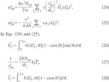
The actual magnitude of the total SDHA as the function of the electronic concentration for the IGA well is presented in Fig. 2共a兲. In this figure we fixed the impurity concentra-tion to be Nim⫽1011cm⫺2. Despite the different behavior of
the angle for systems with attractive and repulsive impuri-ties, both demonstrate quite measurable magnitudes. Figure 2共b兲 clearly shows that the skew-scattering mechanism domi-nates for systems both with attractive and repulsive impuri-ties up to the very high concentrations of the 2-D electrons. In addition, one can manipulate the effect in 2-D systems with a variation of the well width. The impact of the well width on the skew-scattering mechanism is discussed in de-tail in Ref. 18. The main result is the following: the effect always decreases when the well width increases. The depen-dencies of the total 共SDHA兲 on the well width for the IGA wells are demonstrated in Fig. 3. The figure shows that the side-jump contribution can make the effect stable for the well width variations in the case of the attractive impurities. The SOI is known to be larger in narrow-gap semicon-ductors. For this reason, we show in Fig. 4, as an example, the calculation results for the IS wells. We consider here only the QWs with repulsive impurities, in which we can expect 共as it follows from the IGA wells兲 the most interesting result. In this case the total SDHA reaches about 2.5⫻10⫺3rad for the relatively narrow wells, and it increases when the elec-tron concentration increases.
These results show how one can manipulate the forma-tion of the effect mechanisms and magnitude as well by means of changes in the system parameters (n,Nim,L). This
possibility makes properties of the SDHE in 2-D
semicon-ductor systems essentially different from those in the bulk. In three-dimensional systems, we only can manipulate Nim. In
addition, we notice that the SDHA in the QWs is signifi-cantly larger 共in few orders兲 than it was for the bulk 共see Refs. 30, 31, and 36兲. In addition, the effect is easily tunable in QWs.
V. CONCLUSIONS
We described theoretically the SDHE in semiconductor QWs when the 2-D electrons are scattered and form the screened Coulomb centers located in the center of the wells. The one-electronic-band effective Hamiltonian and SO cou-pling potential of the impurities allow us to solve the 2-D spin-dependent Boltzmann equation and to calculate the SDHA at zero magnetic field. We have found large SDHAs for AlInAs/InGaAsAs/AlInAs and CdTe/InSb/CdTe sym-metrical QWs. For instance, in the CdTe/InSb/CdTe narrow QWs the SDHE can reach 2.5⫻10⫺3rad. This could be de-tected in the measurements of the Hall effect at low tempera-tures, and this is potentially useful in integrated electron
FIG. 2.共a兲 The absolute value of the SDHA in the IGA QW and 共b兲 the ratio
as the function of the electron concentration (Nim⫽10
11cm⫺3, L
⫽20 nm; a: Z⫽⫺1, b: Z⫽⫹1).
FIG. 3.共a兲 The absolute value of the SDHA in the IGA QW and 共b兲 the ratio
as the function of the well width (n⫽Nim⫽10 11
cm⫺3; a: Z⫽⫺1, b: Z
⫽⫹1).
FIG. 4. The absolute value of the SDHA in the IS QW with repulsive impurities as the function of the well width (Nim⫽1011cm⫺3, a: n⫽5 ⫻1010cm⫺3, b: n⫽1011cm⫺3).
spin-polarization devices based on semiconductor hetero-structures. It also can be used as a tool of determination of spin-coupling parameters in III-V narrow-gap semiconductor heterostructures. We suggest that experimental investigations should be conducted to verify our theory predictions. ACKNOWLEDGMENTS
This work was supported by the National Science Coun-cil of R.O.C. under contract NSC-92-2112-M-009-015..
1
S. Datta and B. Das, Appl. Phys. Lett. 56, 665共1990兲.
2
G. A. Prinz, Science 282, 1660共1998兲.
3J. Fabian and S. Das Sarma, J. Vac. Sci. Technol. B 17, 1708共1999兲. 4M. E. Flatte´, J. M. Hyers, and W. H. Lau, Spin Dynamics in
Semiconduc-tors, in Semiconductor Spintronics and Quantum Computation, edited by
D. D. Awschalom, D. Loss, and N. Samarth共Springer, Berlin, 2002兲, pp. 107–145.
5J. E. Hirsch, Phys. Rev. Lett. 83, 1834共1999兲. 6G. Gergmann, Phys. Rev. B 63, 193101共2001兲.
7S. Zhang, Phys. Rev. Lett. 85, 393共2000兲; J. Appl. Phys. 89, 7564 共2001兲. 8
A. Cre´pieux and P. Bruno, Phys. Rev. B 64, 0114416共2001兲.
9R. Karplus and J. M. Luttinger, Phys. Rev. 95, 1154共1954兲. 10L. Berger, Phys. Rev. B 2, 4559共1970兲.
11J. Smit, Physica共Amsterdam兲 21, 877 共1955兲; 24, 39 共1958兲. 12
Y. A. Bychkov and E. I. Rashba, Pis’ma Zh. Eksp. Teor. Fiz. 39, 66共1984兲
关JETP Lett. 39, 78 共1984兲兴.
13M. I. D’yakonov and V. Yu. Kachorovskii, Fiz. Tekh. Poluprovodn. 20,
178共1986兲 关Sov. Phys. Semicond. 20, 100 共1986兲兴.
14V. M. Edelstein, Physica B 284–288, 1217共2000兲. 15
T. P. Pareek and P. Bruno, Pramana, J. Phys. 57, 1共2002兲.
16E. Chen, O. Voskoboynikov, and C. P. Lee, Solid State Commun. 125, 381
共2003兲.
17R. S. Silsbee, Phys. Rev. B 63, 155305共2001兲. 18
H. C. Huang, O. Voskobounikov, and C. P. Lee, Phys. Rev. B 67, 195337
共2003兲.
19F. Stern and W. E. Howard, Phys. Rev. 163, 816共1967兲.
20G. Bastard, Wave Mechanics Applied to Semiconductor Heterostructures
共Editions de Physique, Les Ulis, 1990兲.
21E. A. de Andrada e Silva, G. C. La Rocca, and F. Bassani, Phys. Rev. B
55, 16 293共1997兲.
22
Th. Scha¨pers, G. Engels, J. Lange, Th. Klocke, M. Hollfelder, and H. Lu¨th, J. Appl. Phys. 83, 4324共1998兲.
23T. Ando, A. B. Fowler, and F. Stern, Rev. Mod. Phys. 54, 437共1982兲. 24D. K. Ferry and S. M. Goodnick, Transport in Nanostructures共Cambridge
University Press, Cambridge, UK, 1997兲.
25C. J. Joachain, Quantum Collision Theory 共North-Holland, Amsterdam,
1979兲.
26A. G. Sitenko, Scattering Theory共Springer, Berlin, 1990兲.
27F. Cologero, Variable Phase Approach to Potential Scattering共Academic,
New York, 1967兲.
28
O. Voskoboynikov, H. C. Huang, C. P. Lee, and O. Tretyak, Physica E
共Amsterdam兲 12, 252 共2002兲.
29
N. F. Mott and H. S. Massey, The Theory of Atomic Collisions, 3rd ed.
共Oxford University Press, Oxford, UK, 1987兲.
30V. N. Abakumov and I. N. Yassievich, Zh. Eksp. Teor. Fiz. 61, 2571
共1972兲 关Sov. Phys. JETP 34, 1375 共1972兲兴.
31V. N. Abakumov, V. V. Akulinichev, and I. N. Yassievich, Fiz. Thekh.
Poluprovod. 9, 936共1975兲 关Sov. Phys. Semicond. 9, 612 共1975兲兴.
32P. M. Levy, Phys. Rev. B 38, 6779共1988兲. 33
S. L. Chuang, Physics of Optoelectronic Devices 共Wiley-Interscience, New York, 1995兲.
34
E. T. Yu, J. O. McCaldin, and T. C. McGill, Solid State Phys. 46, 2共1992兲.
35Handbook Series on Semiconductor Parameters, edited by M.
Levinsh-tein, S. Rumyantsev, and M. Shur共World Scientific, Singapore, 1999兲.
36J. N. Chazalviel and I. Solomon, Phys. Rev. Lett. 29, 1676共1972兲.
1923 J. Appl. Phys., Vol. 95, No. 4, 15 February 2004 Huang, Voskoboynikov, and Lee