Study on the interface thermal stability of metal-oxide-semiconductor structures by
inelastic electron tunneling spectroscopy
Chih-Feng Huang, Bing-Yue Tsui, Pei-Jer Tzeng, Lurng-Shehng Lee, and Ming-Jinn Tsai
Citation: Applied Physics Letters 88, 262909 (2006); doi: 10.1063/1.2219140 View online: http://dx.doi.org/10.1063/1.2219140
View Table of Contents: http://scitation.aip.org/content/aip/journal/apl/88/26?ver=pdfcov Published by the AIP Publishing
Articles you may be interested in
Aluminum, oxide, and silicon phonons by inelastic electron tunneling spectroscopy on metal-oxide-semiconductor tunnel junctions: Accurate determination and effect of electrical stress
J. Appl. Phys. 96, 5042 (2004); 10.1063/1.1775299
Thermal stability of epitaxial Pt films on Y 2 O 3 in a metal-oxide–Si structure Appl. Phys. Lett. 83, 4758 (2003); 10.1063/1.1632541
Interface characterization of Si 3 N 4 /Si/GaAs heterostructures after high temperature annealing J. Vac. Sci. Technol. B 16, 3032 (1998); 10.1116/1.590338
Microcrystalline oxide-incorporated new diffusion barrier for dynamic random access memory and ferroelectric random access memory capacitor electrode
J. Vac. Sci. Technol. A 15, 2781 (1997); 10.1116/1.580823 Thermal stability of Si 3 N 4 /Si/GaAs interfaces
Appl. Phys. Lett. 70, 1263 (1997); 10.1063/1.118547
This article is copyrighted as indicated in the article. Reuse of AIP content is subject to the terms at: http://scitation.aip.org/termsconditions. Downloaded to IP: 140.113.38.11 On: Thu, 01 May 2014 01:56:26
Study on the interface thermal stability of metal-oxide-semiconductor
structures by inelastic electron tunneling spectroscopy
Chih-Feng Huanga兲 and Bing-Yue Tsui
Department of Electronics Engineering, National Chiao Tung University, 1001 Ta-Hsueh Road, Hsinchu, Taiwan 300, Republic of China and Institute of Electronics, National Chiao Tung University, 1001 Ta-Hsueh Road, Hsinchu, Taiwan 300, Republic of China
Pei-Jer Tzeng, Lurng-Shehng Lee, and Ming-Jinn Tsai
Electronics Research and Service Organization, Industrial Technology Research Institute, Chutung, Hsinchu, Taiwan 310, Republic of China
共Received 25 November 2005; accepted 1 June 2006; published online 30 June 2006兲
The bias polarity-dependent inelastic electron tunneling spectroscopy is employed to detect the thermal stability of the Ta– Pt/ SiO2/ Si and Ta– Pt/ HfO2/ Si structures. This work provides a direct evidence that the Fermi-level pinning of metal gates is counted for the generation of extrinsic states due to interface interaction. A Ta2O5 layer forms at the Ta– Pt/ SiO2 interface during thermal annealing whereas only an intermittent Ta–O bond is observed at the Ta– Pt/ HfO2 interface. Although the heat of formation of HfO2is lower than that of SiO2, Si presumably diffuses into HfO2 layer and replaces Hf atoms during the high-temperature annealing. © 2006 American Institute of
Physics. 关DOI:10.1063/1.2219140兴
Metal gates are expected to replace polysilicon gates and to integrate with high dielectric constant materials beyond 45 nm technology node.1Several kinds of metal gates such as pure metals, binary alloys, metal nitrides, and metal sili-cides have been proposed.2–8One of the most important is-sues with those gates is that the effective work function 共m,eff兲 is thermally unstable. It is suspected that the thermal
instability of m,eff is caused by the interface reaction
be-tween metal electrode and gate dielectric.4–8 However, no direct evidence has been reported because interface analysis is more difficult than surface analysis. The typical analysis techniques such as Fourier transform infrared spectroscopy, x-ray photoelectron spectroscopy, secondary ion mass spec-troscopy, and electron spin resonance spectroscopy may not be suitable for interface analysis on a real device structure.
Recently, a promising interface analysis technique called inelastic tunneling spectroscopy 共IETS兲 was employed to analyze the chemical bonds at the electrode and dielectric interface by detecting the interaction between tunneling elec-trons and phonons.9–11The IETS can further detect the inter-face bonding near the upper interinter-face or lower interinter-face of a metal-insulator-semiconductor 共MIS兲 or metal-insulator-metal structure by using the bias polarity-dependent characteristic.11 In this work, the polarity-dependent IETS technique is used to probe the thermal stability of Ta–Pt alloy/SiO2/ Si and Ta–Pt alloy/HfO2/ Si MIS structures.
The MIS capacitors were fabricated on 共100兲-oriented,
p-type silicon wafers with a resistivity of lower than
0.001⍀ cm. The metal electrode area was 0.024 cm2. The capacitors have a shape of two concentric rings isolated by a thick thermally grown field oxide共FOX兲 in order to keep a uniform electric field as shown in Fig. 1. After field oxide patterning, wafers were cleaned by the standard cleaning process followed by dipping in HF solution for 10 s. For the SiO2 samples, a 1.5 nm thick SiO2 layer was thermally grown in a mixture of N2 and O2 at 700 ° C for 1 min
fol-lowed by annealing in N2 ambient at 900 ° C for 10 min in the same furnace. For the HfO2samples, a 3 nm thick HfO2 layer was deposited at 300 ° C using HfCl4 as precursor and H2O vapor as oxidant in an atomic layer deposition system. No HfO2 postdeposition annealing was followed immedi-ately. Metal gates were patterned by lift-off process. The Ta–Pt alloy was deposited in a cosputtering system to a thickness of 55 nm, and the sputtering powers of Ta and Pt targets were set to dc 30 W and rf 30 W, respectively. After the lift-off process, post-metal-annealing was performed at 500 or 800 ° C in N2ambience for 30 s in the rapid thermal annealing system. This was followed by substrate contact opening using conventional lithography and wet etching pro-cesses. Finally, a 500 nm thick aluminum共Al兲 layer was de-posited as local interconnects and probing pads by thermal evaporation. The IETS measurement was performed by a modulation technique using a lock-in amplifier. The details of the system setup can be found elsewhere.12Measurement was performed at 15 K and the ac modulation is 2 mV with a frequency of 5 KHz. The dc resolution is 2 mV.
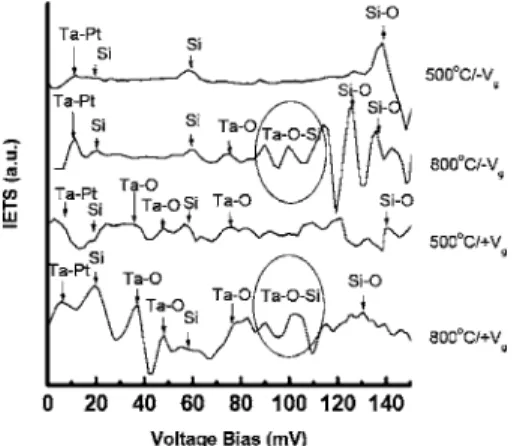
The IETS spectra of 500 and 800 ° C annealed Ta– Pt/ SiO2/ Si samples are shown in Fig. 2. The
asymmet-a兲Electronic mail: [email protected] FIG. 1. The schematic top view and cross section of the test structure.
APPLIED PHYSICS LETTERS 88, 262909共2006兲
0003-6951/2006/88共26兲/262909/3/$23.00 88, 262909-1 © 2006 American Institute of Physics
This article is copyrighted as indicated in the article. Reuse of AIP content is subject to the terms at: http://scitation.aip.org/termsconditions. Downloaded to IP: 140.113.38.11 On: Thu, 01 May 2014 01:56:26
ric IETS was caused by different bias polarities. The nega-tive gate bias qualitanega-tively reflects the interaction between electrons and phonons near the bottom interface.11 The sig-nals of Si substrate and SiO2phonon modes have been well identified and analyzed by previous researchers.11,13The sig-nals of Si phonons were at 20 and 59 mV and the sigsig-nals of SiO2 phonons ranged broadly from 130 to 170 mV.9,11,14 Several additional peaks occurred on the 800 ° C annealed sample共800 °C/−Vgin Fig. 2兲. The peak at 77 mV 共equal to
640 cm−1兲 was attributed to amorphous Ta
2O5.15,16The ob-servation proved the reaction between Ta of Ta–Pt alloy and SiO2. The obvious and intense peaks between 90 and 120 mV were qualitatively attributed to deteriorated SiO2 in-stead of Ta2O5since the main peak of Ta–O was located only at 77 mV. Those peaks between Ta–O modes and Si–O modes represent Ta–O–Si 共metal–O–Si兲 bonds or imperfect SiO2共SiOx兲 due to the chemical reaction between Ta–Pt gate
and SiO2.17,18 The spectra at positive gate bias were more sensitive to the phonon interaction near the Ta–Pt alloy gate. In addition to the Ta–O peak at 77 mV, the other Ta–O peaks at 38 and 49 mV were also observed.11,12Both the 500 and 800 ° C samples revealed Ta–O bond and the higher and sharper peaks of the 800 ° C annealed sample indicated the growth of tantalum oxide.
To investigate the electrical effects of chemical reaction at the interface between Ta–Pt and SiO2, the work function of Ta–Pt gate was analyzed. In Fig. 3, the barrier height of Ta–Pt electrode extracted by the Fowler-Nordheim tunneling plot increases from 3.18 to 3.65 eV as the annealing tem-perature increases from 500 to 800 ° C. The inset shows that
the equivalent oxide thickness is almost unchanged after 800 ° C annealing while the flatband voltage 共Vfb兲 changes from the −0.69 to − 0.48 V. These observations imply that the effective work function is increased after 800 ° C anneal-ing and is consistent with the published data that low work function 共near the silicon conduction band兲 of metal gate tends to the midgap of silicon energy band after high-temperature annealing.7 It is believed that the Fermi-level pinning共work function offset兲 originates from the chemical reaction between metal gate and SiO2 gate dielectric.
Figure 4 shows the IETS spectra of the Ta– Pt/ HfO2/ Si samples annealed at 500 and 800 ° C. Both the negative and positive biased IETS spectra were measured. The peaks were identified based on the literature values.12,17,18The peaks of Si–O and Hf–O–Si vibration modes of the 500 ° C annealed sample were weaker than those of the 800 ° C annealed sample, and those of the negative-gate-bias IETS spectra were stronger than those of the positive ones. These obser-vations imply the growth of silicon oxide at the lower inter-face during high-temperature annealing, which has been clearly detected by the transmission electron microscope 共TEM兲 inspection. The shift of the main peak of Hf–O vibra-tion modes after high-temperature annealing was reasonably caused by the crystallization, where the main peak of the 500 ° C annealed sample was located at 32 mV and was lower than the main peak of the 800 ° C annealed sample located at 43 mV.18 A special peak of the Hf–O vibration mode at 71 mV observed on both the 500 and 800 ° C an-nealed samples was attributed to the hafnium silicate but not to pure HfO2.17,19This implied that the interfacial layer con-tained the mixture of Hf–O and O–Si bonds, i.e., Hf silicate. Another special peak at 38 mV was suspected to the Ta–O vibration mode and was only observed on the positive-gate-bias IETS spectra.20 The peak was small and did not grow even after high-temperature annealing. The Ta– Pt/ HfO2 interface was further inspected by high resolution transmis-sion electron microscopy. An intermittent monolayer mate-rial was observed at the interface which corresponded to the weak IETS peaks of both 500 and 800 ° C samples. The monolayer Ta–O bond might be formed during the Ta–Pt alloy deposition.
The reaction at the upper interface of HfO2 is self-limited while the reaction at the lower interface of HfO2 is continuous during the high-temperature annealing. The reac-tant, oxygen, surely does not come from the annealing am-bient since the Ta–Pt alloy is not oxidized at the upper inter-FIG. 2. The inelastic electron tunneling spectra of Ta– Pt/ SiO2/degenerated
Si samples annealed at 500 and 800 ° C.
FIG. 3. Fowler-Nordheim plot of the Ta– Pt/ SiO2 共5.5 nm兲/Si structure
after annealing at 500 and 800 C for 30 ° C. The m*/ m
o= 0.26 is used to
calculate the barrier height共⌽B兲 共Ref. 24兲. The inset shows the relative
C-V curves.
FIG. 4. The inelastic electron tunneling spectra of Ta– Pt/ HfO2/degenerated
Si samples annealed at 500 and 800 ° C.
262909-2 Huang et al. Appl. Phys. Lett. 88, 262909共2006兲
This article is copyrighted as indicated in the article. Reuse of AIP content is subject to the terms at: http://scitation.aip.org/termsconditions. Downloaded to IP: 140.113.38.11 On: Thu, 01 May 2014 01:56:26
face. Those mean that the oxygen should come from the HfO2layer. The existence of Hf silicate sensibly implies that the oxygen comes from the broken Hf–O bond. However, the postulation that HfO2 releases oxygen atoms during high-temperature annealing while the oxygen only reacts with Si but not Ta is unreasonable since the heat of formations of HfO2, Ta2O5, and SiO2are −271, −230, and −210 Kcal/ mol, respectively. Besides, the Hf–O, Ta–O, and Si–O bonds are more stable than the Si–Si bond since the bonding energies of Hf–O, Ta–O, Si–O, and Si–Si are 801.7, 799.1, 799.6, and 326.8 KJ/ mol, respectively.21 Therefore, it is presumed that the oxygen is not thermally decomposed from the HfO2, but it is more reasonable that the Si atom diffuses into the HfO2 layer from the Si substrate and directly replaces the Hf atom.21–23 On the other hand, it is difficult for Ta atom to diffuse into the HfO2 layer, and HfO2 is more stable than Ta2O5 so that only an intermittent Ta–O bond forms at the Ta– Pt/ HfO2interface. While the Ta–Pt alloy is deposited on the SiO2, the lower heat of formation of Ta2O5 than that of SiO2 results in a more stable Ta2O5.
In summary, IETS spectroscopy provides a direct inspec-tion of thermal instability at the interface of the MIS struc-ture. The analysis of results provides a direct evidence that the Fermi-level pinning of Ta–Pt metal gates on SiO2 is counted for the generation of extrinsic states due to the for-mation of the tantalum oxide. The Ta– Pt/ HfO2 interface is more thermally stable than the HfO2/ Si interface. Hf silicate formation during thermal annealing is detected at the latter interface by our IETS analysis.
This work is supported by the National Science Council of Taiwan, Republic of China under Contract No. NSC-94-2215-E-009-004.
1International Technology Roadmap for Semiconductors 共ITRS兲, 2003
Edition 共Semiconductor Industry Association 共SIA兲, 2003兲, http:// public.itrs.net
2D. Ha, P. Ranade, Y.-K. Choi, J.-S. Lee, T.-J. King, and C. Hu, Jpn. J.
Appl. Phys., Part 1 42, 1979共2003兲.
3P. Xuan and J. Bokor, IEEE Electron Device Lett. 24, 634共2003兲. 4B.-Y. Tsui and C. F. Huang, IEEE Electron Device Lett. 24, 153共2003兲. 5J. Westlinder, T. Schram, L. Pantisano, E. Cartier, A. Kerber, G. S. Lujan,
J. Olsson, and G. Groeseneken, IEEE Electron Device Lett. 24, 550 共2003兲.
6C. Ren, H. Y. Yu, J. F. Kang, Y. T. Hou, M.-F. Li, W. D. Wang, D. S. H.
Chan, and D.-L. Kwong, IEEE Electron Device Lett. 25, 123共2004兲.
7H. Y. Yu, C. Ren, Y.-C. Yeo, J. F. Kang, X. P. Wang, H. H. H. Ma, M.-F.
Li, D. S. H. Chan, and D.-L. Kwong, IEEE Electron Device Lett. 25, 337 共2004兲.
8M. S. Joo, B. J. Cho, N. Balasubramanian, and D.-L. Kwong, IEEE
Elec-tron Device Lett. 25, 716共2004兲.
9W.-K. Lye, E. Hasegawa, T.-P. Ma, R. C. Barker, Y. Hu, J. Kuehne, and D.
Frystak, Appl. Phys. Lett. 71, 2523共1997兲.
10P. Balk, S. Ewert, S. Schmitz, and A. Steffen, J. Appl. Phys. 69, 6510
共1991兲.
11W. He and T. P. Ma, Appl. Phys. Lett. 83, 2605共2003兲.
12Y. Wang, R. R. Mallik, and P. N. Henriksen, Rev. Sci. Instrum. 64, 890
共1993兲.
13A. G. Chynoweth, R. A. Logan, and D. E. Thomas, Phys. Rev. 125, 877
共1962兲.
14G. Salace, C. Petit, and D. Vuilaume, J. Appl. Phys. 91, 5896共2002兲. 15R. A. B. Devine, Appl. Phys. Lett. 68, 1924共1996兲.
16H. Ono and K.-I. Koyanagi, Appl. Phys. Lett. 77, 1431共2000兲. 17K. T. Queeney, M. K. Weldon, J. P. Chang, Y. J. Chabal, A. B. Gurevich,
J. Sapjeta, and R. L. Opila, J. Appl. Phys. 87, 1322共2000兲.
18D. A. Neumayer and E. Cartier, J. Appl. Phys. 90, 1801共2001兲. 19M. A. Quevedo-Lopez, J. J. Chambers, M. R. Visokay, A. Shanware, and
L. Colombo, Appl. Phys. Lett. 87, 12902共2005兲.
20D.-G. Park, T.-H. Cha, K.-Y. Lim, H.-J. Cho, T.-K. Kim, S.-A. Jang, Y.-S.
Suh, V. Misra, I.-S. Yeo, J.-S. Roh, J. W. Park, and H.-K. Yoon, Tech. Dig. - Int. Electron Devices Meet. 2001, 671.
21Periodic table of elements by The University of Sheffield and
WebEle-ments Ltd., UK, http://www.webeleWebEle-ments.com/
22T. H. Moo, M.-H. Ham, and J.-M. Myoung, Appl. Phys. Lett. 86, 102903
共2005兲.
23J.-C. Lee, S.-J. Oh, M. Cho, C. S. Hwang, and R. Jung, Appl. Phys. Lett. 84, 1305共2004兲.
24D. K. Schroder, Semiconductor Material and Device Characterization,
2nd ed.共Wiley, New York, 1998兲, p. 393.
262909-3 Huang et al. Appl. Phys. Lett. 88, 262909共2006兲
This article is copyrighted as indicated in the article. Reuse of AIP content is subject to the terms at: http://scitation.aip.org/termsconditions. Downloaded to IP: 140.113.38.11 On: Thu, 01 May 2014 01:56:26