DOI: 10.1126/science.1216511
, 1007 (2012);
336
Science
et al.
Hsiang-Yao Hsiao
Nanotwinned Copper
This copy is for your personal, non-commercial use only.
clicking here.
colleagues, clients, or customers by
, you can order high-quality copies for your
If you wish to distribute this article to others
here.
following the guidelines
can be obtained by
Permission to republish or repurpose articles or portions of articles
):
April 28, 2014
www.sciencemag.org (this information is current as of
The following resources related to this article are available online at
http://www.sciencemag.org/content/336/6084/1007.full.html
version of this article at:
including high-resolution figures, can be found in the online
Updated information and services,
http://www.sciencemag.org/content/suppl/2012/05/23/336.6084.1007.DC1.html
can be found at:
Supporting Online Material
http://www.sciencemag.org/content/336/6084/1007.full.html#ref-list-1
, 8 of which can be accessed free:
cites 17 articles
This article
http://www.sciencemag.org/content/336/6084/1007.full.html#related-urls
1 articles hosted by HighWire Press; see:
cited by
This article has been
http://www.sciencemag.org/cgi/collection/mat_sci
Materials Science
subject collections:
This article appears in the following
is a
Science
2012 by the American Association for the Advancement of Science; all rights reserved. The title
Copyright
American Association for the Advancement of Science, 1200 New York Avenue NW, Washington, DC 20005.
(print ISSN 0036-8075; online ISSN 1095-9203) is published weekly, except the last week in December, by the
Science
on April 28, 2014
www.sciencemag.org
Downloaded from
on April 28, 2014
www.sciencemag.org
Downloaded from
on April 28, 2014
www.sciencemag.org
Downloaded from
on April 28, 2014
www.sciencemag.org
Downloaded from
on April 28, 2014
www.sciencemag.org
Downloaded from
absent when the superconductor is replaced by a normal conductor. Based on these observa-tions, we conclude that our spectroscopy ex-periment provides evidence for the existence of Majorana fermions.
Improving the electron mobility and opti-mizing the gate coupling will enable us to map out the phase diagram of the topological super-conductor in the plane ofEZandm (27–30). It
will be interesting to control the subband occu-pation underneath the superconductor down to a single subband to make direct comparisons to theoretical models. Currently, we probe induced gaps and states from all occupied subbands, each with a different coupling to the tunnel barrier. The topological state in the topmost subband likely has the weakest coupling to the tunnel barrier. Single-subband models (8, 9) predict that one should observe a closing of the topo-logical gap; however, in multisubband systems, this gap closing may not be visible. The constant gap in Fig. 2 may come from lower subbands. The presence of multiple subbands together with our finite temperature may also be the reason that our ZBP is currently only ~5% of the theoretical zero-temperature limit of2e2/h (12, 14).
Finally, we note that this work does not address the topological properties of Majorana fermions. The first step toward demonstrating topological protection would be the observa-tion of conductance quantizaobserva-tion (12, 32). Sec-ond, in a Josephson tunnel junction with phase differenceϕ and a pair of Majoranas on either side, the current-phase relation becomes pro-portional to sin(ϕ/2). The factor 2 is another distinct Majorana signature, which should be observable as an h/e flux periodicity in a
superconducting quantum interference device measurement (8, 9). The last type of experiment involves the exchange of Majoranas around each other. Such braiding experiments can reveal their non-Abelian statistics, which are the ultimate proof of topologically protected Majorana fer-mions (33–35).
References and Notes
1. E. Majorana, Soryushiron Kenkyu (Engl. transl.) 63, 149 (1981) [translation from Nuovo Cimento 14, 171 (1937)].
2. F. Wilczek, Nat. Phys. 5, 614 (2009). 3. M. Franz, Physics 3, 24 (2010). 4. A. Yu. Kitaev, Phys. Usp. 44, 131 (2001). 5. L. Fu, C. L. Kane, Phys. Rev. Lett. 100, 096407
(2008).
6. J. D. Sau, R. M. Lutchyn, S. Tewari, S. Das Sarma, Phys. Rev. Lett. 104, 040502 (2010). 7. J. Alicea, Phys. Rev. B 81, 125318 (2010). 8. R. M. Lutchyn, J. D. Sau, S. Das Sarma, Phys. Rev. Lett.
105, 077001 (2010).
9. Y. Oreg, G. Refael, F. von Oppen, Phys. Rev. Lett. 105, 177002 (2010).
10. C. W. J. Beenakker, http://arxiv.org/abs/1112.1950 (2011).
11. J. Alicea, http://arxiv.org/abs/1202.1293 (2012). 12. K. T. Law, P. A. Lee, T. K. Ng, Phys. Rev. Lett. 103,
237001 (2009).
13. K. Flensberg, Phys. Rev. B 82, 180516 (2010). 14. J. D. Sau, S. Tewari, R. Lutchyn, T. Stanescu,
S. Das Sarma, Phys. Rev. B 82, 214509 (2010). 15. S. R. Plissard et al., Nano Lett. 12, 1794 (2012). 16. H. A. Nilsson et al., Nano Lett. 9, 3151 (2009). 17. S. Nadj-Perge et al., Phys. Rev. Lett. 108, 166801
(2012).
18. P. W. Brouwer, M. Duckheim, A. Romito, F. von Oppen, Phys. Rev. Lett. 107, 196804 (2011).
19. J. D. Sau, S. Tewari, S. Das Sarma, Phys. Rev. B 85, 064512 (2012).
20. See supplementary materials on Science Online. 21. J. D. Pillet et al., Nat. Phys. 6, 965 (2010). 22. T. Dirks et al., Nat. Phys. 7, 386 (2011).
23. H. le Sueur, P. Joyez, H. Pothier, C. Urbina, D. Esteve, Phys. Rev. Lett. 100, 197002 (2008).
24. S. Sasaki et al., Nature 405, 764 (2000).
25. M. Zareyan, W. Belzig, Yu. V. Nazarov, Phys. Rev. B 65, 184505 (2002).
26. B. J. van Wees, P. de Vries, P. Magnée, T. M. Klapwijk, Phys. Rev. Lett. 69, 510 (1992).
27. M. Wimmer, A. R. Akhmerov, M. V. Medvedyeva, J. Tworzydło, C. W. Beenakker, Phys. Rev. Lett. 105, 046803 (2010).
28. A. C. Potter, P. A. Lee, Phys. Rev. Lett. 105, 227003 (2010).
29. R. M. Lutchyn, T. D. Stanescu, S. Das Sarma, Phys. Rev. Lett. 106, 127001 (2011).
30. T. D. Stanescu, R. M. Lutchyn, S. Das Sarma, Phys. Rev. B 84, 144522 (2011).
31. P. Středa, P. Šeba, Phys. Rev. Lett. 90, 256601 (2003).
32. M. Wimmer, A. R. Akhmerov, J. P. Dahlhaus, C. W. J. Beenakker, N. J. Phys. 13, 053016 (2011). 33. N. Read, D. Green, Phys. Rev. B 61, 10267 (2000). 34. D. A. Ivanov, Phys. Rev. Lett. 86, 268 (2001). 35. C. Nayak, S. H. Simon, A. Stern, M. Freedman,
S. Das Sarma, Rev. Mod. Phys. 80, 1083 (2008). Acknowledgments: We thank D. Thoen and T. Klapwijk for sharing their NbTiN technology and A. Akhmerov, J. Alicea, C. Beenakker, M. Freedman, F. Hassler, G. Immink, H. Keijzers, C. Marcus, S. Nadj-Perge, Y. Nazarov, I. van Weperen, M. Wimmer, and D. van Woerkom for discussions and assistance. This work has been supported by European Research Council, Netherlands Organization for Scientific Research (NWO), Foundation for Fundamental Research on Matter (FOM), and Microsoft Corporation Station Q. Supplementary Materials www.sciencemag.org/cgi/content/full/science.1222360/DC1 Supplementary Text Figs. S1 to S14 References (36, 37) Data Files
23 March 2012; accepted 5 April 2012 Published online 12 April 2012; 10.1126/science.1222360
Unidirectional Growth of
Microbumps on (111)-Oriented and
Nanotwinned Copper
Hsiang-Yao Hsiao,1Chien-Min Liu,1Han-wen Lin,1Tao-Chi Liu,1Chia-Ling Lu,1 Yi-Sa Huang,1Chih Chen,1* K. N. Tu2*
Highly oriented [111] Cu grains with densely packed nanotwins have been fabricated by direct-current electroplating with a high stirring rate. The [111]-oriented and nanotwinned Cu (nt-Cu) allow for the unidirectional growth of Cu6Sn5intermetallics in the microbumps of
three-dimensional integrated-circuit packaging; a uniform microstructure in a large number of microbumps of controlled orientation can be obtained. The high-density twin boundaries in the nt-Cu serve as vacancy sinks during the solid-state reaction between Pb-free solder and Cu and greatly reduce the formation of Kirkendall (or Frenkel) voids.
A
change from two-dimensional to three-dimensional integrated circuits (3D IC) is under way in the microelectronics in-dustry as the limits of very-large-scale integration in silicon chip technology are approached (1). In essence, 3D IC is intended to bring packagingtechnology and chip technology together. With respect to scaling the density of solder bumps on a chip surface, the diameter of a flip-chip solder bump is about 100mm today, and it should be possible to reduce this to 1mm. This improve-ment will increase the density of bumps per unit
area by 4 orders of magnitude, yet the solder volume will be reduced by 6 orders of magni-tude. However, the melting point of the solder remains unchanged, meaning that each micro-bump may contain only a few grains after process-ing. Variation in the grain orientation may lead to a wide distribution of the orientation-dependent properties of microbumps, which may in turn lead to early failure and low reliability. This is because certain grain orientations allow fast dif-fusion and electromigration (2, 3). Because there are a large number of microbumps on a stack of chips in a 3D IC, achieving a uniform structure in several thousand of these micro-bumps on each chip is a critical issue.
Maintaining control over the microstructure of the microbumps is nontrivial because of
1Department of Materials Science and Engineering, National Chiao Tung University, Hsinchu, Taiwan 30010, Republic of China.2Department of Materials Science and Engineering, University of California at Los Angeles, Los Angeles, CA 90095, USA.
*To whom correspondence should be addressed. E-mail: chih@mail.nctu.edu.tw (C.C.); kntu@ucla.edu (K.N.T.)
reflow. Reflow means that the solder bump is melted to achieve chip-to-chip or chip-to-substrate joints. It is very difficult to control the solid-state microstructure as a molten solder bump solidi-fies; typically, the grains are randomly oriented. Furthermore, during the solid-state aging of the microbumps, the solder will transform into inter-metallic compounds. These compounds will
dom-inate the properties of the microbumps because the solder thickness decreases to about 10mm or less in microbumps to connect the through-Si-vias (TSVs).
We report that using [111]-oriented nano-twinned Cu (nt-Cu) as the under-bump metal-lization promotes the unidirectional growth of intermetallic compounds in a large number of
microbumps, leading to a uniform microstruc-ture of all the microbumps. Unidirectional growth recalls the single-crystal turbine blades of a superalloy, requiring a crystal seed and a temper-ature gradient (4). To seed thousands of indi-vidual microbumps on a chip is impractical. Instead, we report a method of unidirectional growth that uses reactive epitaxial growth of Fig. 1. The microstructural characterization of the
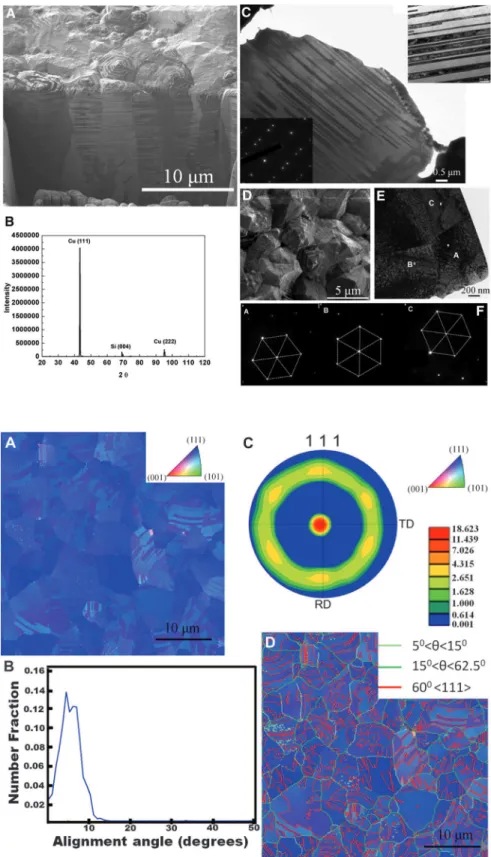
electroplated Cu at a current density of 80 mA/cm2for 30 min at a stirring speed of 1200 rpm. (A) Cross-sectional FIB micrograph. (B) X-ray diffraction. (C) Cross-sectional image showing the Cu nanotwins near the cone. (D) Plan-view FIB micrograph. (E) Plan-view TEM image. (F) Diffraction patterns of the three grains in (E).
Fig. 2. EBSD analysis of the nt-Cu. (A) Plan-view inverse pole figure maps of the Cu surface. Color coding displays the out-of-plan direction in terms of the inverse pole figure. (B) Number fraction of the Cu grains deviated from [111] as a function of angle. (C) {111} pole figures of the fabricated Cu. TD and RD represent transverse direction and rolling direction, respectively. (D) Grain boundary characteristics.
microbumps on [111]-oriented nanotwin Cu. The [111] single crystals of Cu are replaced by [111]-oriented nt-Cu in every microbump.
The small diameter of the microbump enables the growth of only a few oriented grains, and smaller and misoriented grains will be
elimi-nated by ripening. The prerequisite is the prep-aration of oriented (111) nt-Cu as the under-bump metallization in each of thousands of microbumps. We have achieved this by intro-ducing a rapid rotation of the electrolyte in the electroplating of Cu and by adding surfactants in the electrolyte solution.
Randomly oriented nt-Cu has been fabri-cated by using pulsed electroplating (5–7), and it possesses excellent mechanical strength (8–11). It also exhibits a higher electromigration resist-ance than regular Cu grains (12). For these rea-sons, nt-Cu has drawn a great deal of recent attention. Anderoglu et al. reported that nt-Cu with a [111] preferred orientation can be deposited via magnetron sputtering (13). However, in in-terconnect and packaging technology, Cu inter-connects are deposited by electroplating.
In this report, [111]-oriented Cu grains with nt-Cu have been fabricated by dc electroplating with sulfuric acid as the electrolyte. Surfactants are added to the electrolyte, and the stirring speed of the electrolyte, ranging from 600 to 1200 rev-olutions per min (rpm), is critical to the outcome of the electroplating (14).
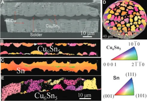
Highly oriented nt-Cu can be fabricated by specific current densities and stirring rates in electrolyte (supplementary materials and figs. S2 and S3). Figure 1A shows the cross-sectional focused ion beam (FIB) image for the nt-Cu electroplated with a current density of 80 mA/cm2 at 1200 rpm for 30 min. The thickness of the Cu film is greater than 20mm, and columnar Cu grains with unidirectional nanotwins are ob-tained (figs. S4 and S5). The normal of all the [111]-oriented nanotwins are aligned nearly par-allel to the film growth direction. X-ray diffrac-tion indicates that these Cu grains possess a very strong [111] preferred orientation (Fig. 1B and fig. S4). We note that many cones appear on the film surface. Spots from twins were observed in Fig. 3. (A) FIB image showing a microbump with 20-mm
nt-Cu under-bump metallizations on both sides. (B) EBSD orientation image maps in the rolling direction for the Cu6Sn5intermetallic compounds. (C)
Orienta-tion image maps for the remaining Sn2.5Ag in the rolling direction. (D) Plan-view orientation image maps in the normal direction for a microbump reflowed at 260°C for 5 min. (E) Another microbump reflowed for 5 min at 260°C.
Fig. 4. Cross-sectional FIB image showing a microbump aged at 150°C (A) for 500 hours and (B) for 1000 hours. (C) Cross-sectional TEM image showing the interface of Cu3Sn and nt-Cu.
the cross-sectional transmission electron micros-copy (TEM) image and the corresponding elec-tron diffraction pattern for the cone microstructure (Fig. 1C). The spacing of the nanotwins ranges from 10 to 100 nm. Figure 1D shows the plan-view FIB image of the cones on the Cu film sur-face. The nanotwins may have nucleated at the tips of the cones. The plan-view TEM and elec-tron diffraction images of one of the cones have been examined to confirm the [111] orientation, and the edges of the cone exhibit sixfold sym-metry. Figure 1E presents the plan-view TEM image for three neighboring (111) grains: A, B, and C in the middle of the sample, prepared by FIB polishing. The corresponding selected area diffraction pattern is shown in Fig. 1F. The rota-tion angle between grains A and B is 22°, whereas it is 15° between grains A and C.
Electron backscatter diffraction (EBSD) was used to analyze the statistical distributions of the grain orientations and the grain boundaries (fig. S1). The orientation image maps of the film surface after polishing by FIB show that the Cu film has a strong {111} texture (Fig. 2A). The corresponding color in the inverse pole figure (Fig. 2) represents the out-of-plane direction, in-dicating a very strong preferred orientation of [111]. The statistical data for the misalignment angles of the Cu (111) grains indicate that 96% of the columnar Cu grains have less than 10° of misalignment with respect to the [111] direction (Fig. 2B). In addition, Fig. 2C shows the frac-tion with the〈111〉 out-of-plane direction in terms of the intensity of the central pole. The high den-sity at the central pole reveals that a very high fraction of the electroplated Cu grains have a 〈111〉 preferred orientation. Figure 2D shows the grain boundaries, including the low, high, and twin boundaries. Here, we define low-angle grain boundaries as those with a misorientation angle less than 15° and high-angle boundaries as those with a misorientation angle between 15° and 65°. A twin boundary is categorized by a 60° angle grain boundary. The results indicate that most of the grain boundaries analyzed can be charac-terized as high-angle boundaries.
Suh reported the orientation relationship be-tween a [001]-oriented Cu single crystal and the Cu6Sn5 grains (15). Zou studied the
ori-entation relationships between the Cu6Sn5grains
and [111]-oriented Cu single crystals (16, 17). We can fabricate oriented nt-Cu in patterned openings and have applied the very strongly oriented [111] nt-Cu to control the orientations of the Cu6Sn5grains in a large number of
mi-crobumps (figs. S5 and S6). Figure 3A shows the cross-sectional FIB image of a microbump between two chips with a 10.5-mm-thick Sn2.5Ag solder after a reflow of 3 min at 260°C. The solder thickness is close to that found in 3D IC packaging. The Cu6Sn5compounds grew on the
(111) planes of the nt-Cu under-bump metalli-zation. The EBSD orientation image maps for the Cu6Sn5compounds indicate a preferred
ori-entation near the (0001) plane of the Cu6Sn5
(Fig. 3B). Figure 3C presents the orientation image maps for the remaining Sn2.5Ag. A plan-view EBSD analysis was also performed to con-firm the preferred orientation of all the Cu6Sn5
compounds on a microbump (Fig. 3D). Almost all the Cu6Sn5 grains have a preferred
orien-tation close to (0001) (fig. S7). In another sam-ple reflowed for 5 min at 260°C, some of the Cu6Sn5grains on the top chip nearly touched
the Cu6Sn5grains on the bottom chip (Fig. 3E).
Upon closer inspection, some have merged into one grain. We observe that two misoriented Cu6Sn5grains on the top and bottom always
merge into one single Cu6Sn5grain, as indicated
by the arrows in the figure.
Lastly, we note that the metallization on oriented nt-Cu forms very few or no Kirkendall (or Frenkel) voids during solid-state aging (18). It has been reported that severe Kirkendall voids form in the Cu3Sn/Cu interface after solid-state
aging in solder joints and greatly weaken the mechanical properties of the joint (19, 20). The cross-sectional FIB image of a microbump after solid-state aging at 150°C for 500 hours (Fig. 4A) shows that the solder has been transformed completely into Cu6Sn5and Cu3Sn. The Cu3Sn
layer is 2.14mm thick, yet only a few voids are observed in the Cu3Sn/Cu interface. After aging
at 150°C for 1000 hours, the Cu3Sn layer
thick-ness grew to 3.12mm (Fig. 4B), and no obvious Kirkendall voids were found (fig. S8). Figure 4C shows the cross-sectional TEM image of the in-terface of Cu3Sn/nt-Cu; some nanotwins end in
Cu3Sn grains. In transforming one molecule of
Cu6Sn5 into two molecules of Cu3Sn, the
re-maining three Sn atoms will attract nine Cu atoms to form three Cu3Sn molecules, and the
vacancies required for the Cu diffusion may condense to form voids. Although the twin boundaries are coherent, there are steps and kinks that can serve as vacancy sinks. In addi-tion, Xuet al. reported that there are butt twins in the electroplated Cu and that they serve as vacancy sinks (21). The high density of nano-twins will provide high density of vacancy sinks. Therefore, no supersaturation of vacancies or nucleation of Kirkendall voids occurs. We expect that the electrical and mechanical properties of the microbumps without Kirkendall voids will be better.
Copper pillars without nanotwins have been implemented in microprocessors to in-crease the electromigration resistance and the performance of heat dissipation (22). The me-chanically strong nanotwinned microbumps may cause a reliability concern because of chip-packaging interaction. In the traditional flip-chip technology, Si dies are bonded to polymer sub-strates, and large thermal stress thus occurs be-cause of the mismatch in thermal expansion coefficients between the two materials. However, in 3D IC, Si dies are bonded to Si substrates of TSV interposers. Therefore, the chip-packaging interaction because of thermal stress is minimized in the microbumps.
By electroplating, we have fabricated highly oriented [111] nt-Cu in columnar [111]-oriented Cu grains in a large number of patterned under-bump metallizations of 20mm diameter on Si wafers. The oriented nt-Cu can induce the uni-directional growth of [0001] Cu6Sn5grains
in solder reflow reactions. In subsequent solid-state aging, the nanotwin boundaries serve as vacancy sinks and prevent the supersatura-tion of vacancies at the interface of Cu3Sn/Cu,
leading to the formation of very few Kirkendall voids.
References and Notes
1. J. C. Lin et al., paper presented at IEEE International Electron Devices Meeting, San Francisco, CA, 6 December 2010.
2. M. Lu, D. Y. Shih, P. Lauro, C. Goldsmith, D. W. Henderson, Appl. Phys. Lett. 92, 211909 (2008).
3. C. Chen, H. M. Tong, K. N. Tu, Annu. Rev. Mater. Res. 40, 531 (2010).
4. D. R. Flack, Fundamentals of Jet Propulsion with Applications (Cambridge Univ. Press, New York, 2005), chap. 8.
5. L. Lu, Y. Shen, X. Chen, L. Qian, K. Lu, Science 304, 422 (2004); 10.1126/science.1092905.
6. L. Lu, X. Chen, X. Huang, K. Lu, Science 323, 607 (2009).
7. X. Li, Y. Wei, L. Lu, K. Lu, H. Gao, Nature 464, 877 (2010).
8. J. Schiøtz, K. W. Jacobsen, Science 301, 1357 (2003).
9. S. J. Zhou, D. L. Preston, P. S. Lomdahl, D. M. Beazley, Science 279, 1525 (1998).
10. L. Lu, M. L. Sui, K. Lu, Science 287, 1463 (2000). 11. K. Lu, L. Lu, S. Suresh, Science 324, 349 (2009). 12. K. C. Chen, W. W. Wu, C. N. Liao, L. J. Chen, K. N. Tu,
Science 321, 1066 (2008).
13. O. Anderoglu et al., Appl. Phys. Lett. 93, 083108 (2008).
14. See supplementary materials on Science Online. 15. J. O. Suh, K. N. Tu, N. Tamura, J. Appl. Phys. 102,
063511 (2007).
16. H. F. Zou, H. J. Yang, Z. F. Zhang, Acta Mater. 56, 2649 (2008).
17. H. F. Zou, H. J. Yang, Z. F. Zhang, J. Appl. Phys. 106, 113512 (2009).
18. Y. Yin et al., Science 304, 711 (2004). 19. K. Zeng et al., J. Appl. Phys. 97, 024508 (2005). 20. R. Labie et al., paper presented at the 3rd Electronic
System-Integration Technology Conference (IEEE Components, Packaging, and Manufacturing Technology Society), Berlin, Germany, 13 September 2010. 21. L. Xu et al., J. Appl. Phys. 104, 113717 (2008). 22. A. Yeoh et al., paper presented at Electronic Components
and Technology Conference (IEEE), San Diego, CA, 30 May 2006.
Acknowledgments: The financial support from the National Science Council, Taiwan, under the contract NSC 98-2221-E-009-036-MY3 is acknowledged. The authors thank J.-C. Kuo at National Cheng Kung University for assistance in the EBSD analysis. A patent,“Electrodeposited nano-twins copper layer and method of fabricating the same,” is under application. The processing conditions of the (111)-oriented nt-Cu have been submitted for a patent application. The rest of the data and figures in this Report have not been presented or published elsewhere.
Supplementary Materials
www.sciencemag.org/cgi/content/full/336/6084/1007/DC1 Materials and Methods
Figs. S1 to S8
11 November 2011; accepted 19 April 2012 10.1126/science.1216511