Low Droop Nonpolar GaN/InGaN Light Emitting Diode Grown
on m-Plane GaN Substrate
Shih-Pang Chang,a,bTien-Chang Lu,a,c,zLi-Fu Zhuo,aChung-Ying Jang,a Da-Wei Lin,aHung-Chih Yang,bHao-Chung Kuo,a and Shing-Chung Wanga a
Department of Photonics and Institute of Electro-Optical Engineering, National Chiao Tung University, Hsinchu 300, Taiwan
b
Epistar Company Limited, Research and Development Division, Hsinchu 300, Taiwan c
Institute of Lighting and Energy Photonics, National Chiao Tung University, Tainan County 711, Taiwan
The low droop nonpolar m-plane InGaN/GaN light emitting diode 共LED兲 has been fabricated and investigated. The external quantum efficiency for a 300⫻ 300 m square LED chip only drops about 18% from maximum at an operation current of 22 A/cm2共20 mA兲 to 330 A/cm2共300 mA兲 dc operations at room temperature. In addition, the internal quantum efficiency has been extracted by temperature-dependent photoluminescence measurements, and there is no droop observed as the carrier density increases. The small droop in efficiency of m-plane LEDs could be due to the lack of polarization effects that enhances the carrier confinement under high current density operation. The polarization anisotropy is clearly observed in the m-plane LED, and the degree of polarization is 68%.
© 2010 The Electrochemical Society. 关DOI: 10.1149/1.3327909兴 All rights reserved.
Manuscript submitted November 10, 2009; revised manuscript received January 20, 2010. Published March 23, 2010.
High efficiency light sources based on III-nitride light emitting diodes 共LEDs兲 are required for the general illumination market, where the driving current of 1 A, corresponding to the current den-sity of 100 A/cm2for a 1 mm2chip, is unavoidable to achieve high
output power. However, for InGaN/GaN multiple-quantum-well 共MQW兲 LEDs, a well-known fundamental problem needs to be overcome: the efficiency droop that describes the reduction in the external quantum efficiency共EQE兲 with the increased operation cur-rent density. Normally, the EQE of the InGaN MQW LED reaches its maximum at ⬃10 A/cm2 and drops to half at ⬃100 A/cm2.
Many mechanisms have been suggested to account for the efficiency droop in InGaN LEDs.1-5To date, there still remains a debate about the main mechanism responsible for the significant efficiency drop at a high current in blue and green LEDs. Nonpolar GaN is one of the important approaches from preventing the efficiency droop that eliminates the quantum-confined Stark effect in the quantum wells 共QWs兲.6,7
In this study, we demonstrate a low droop nonpolar
m-plane LED grown on the freestanding m-plane GaN substrate. For
a 300⫻ 300 m square LED chip, the EQE only drops about 18% from maximum at an operation current of 20–300 mA, correspond-ing to the current density of 330 A/cm2. In addition, the electrical characteristics and polarization of the LED are presented and dis-cussed.
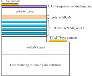
The LEDs were grown by metallorganic chemical vapor deposi-tion on freestanding bulk m-plane GaN substrates made by hydride vapor phase epitaxy. The exposed m-plane surface of these slices was prepared by chemical and mechanical surface treatment tech-niques. The threading dislocation density of the m-plane GaN sub-strate was less than 5⫻ 106 cm2; the carrier concentration was
about 1⫻ 1017 cm3, and the root-mean-square value of the surface roughness was smaller than 1 nm. The growth conditions of the LEDs were very similar to those of the conventional c-plane LEDs. A GaN:Si layer was grown first on top of the substrate without a low temperature nucleation layer, followed by a four-period InGaN/GaN undoped QW active region. The X-ray diffraction /2 measure-ment was performed to examine the well width and to identify the In composition. The thickness of the well and barrier were 2.5 and 10 nm, respectively, and the In composition was about 15% in the LED structure. After the active region was grown, a 20 nm thick p-AlGaN electron-blocking layer was grown on top of the last barrier, fol-lowed by a 200 nm thick p-GaN layer. An annealed SnO2-doped In2O3共indium tin oxide兲 p-type GaN contact was utilized as a
trans-parent p-electrode. LED mesas were etched by reactive ion etching.
Ti/Al/Ti/Au n-contacts were deposited by E-beam evaporation. The LED chip was diced into a 300⫻ 300 m square with a planar type U-shaped n-contact. The n- and p-type GaN have no surface texturing for light extraction. The schematic of the LED structure is shown in Fig.1.
The electrical and luminescence characteristics of the diode were measured by on-wafer probing of the devices, and the optical emis-sion power was measured with a calibrated integrating sphere. All measurements were carried out under dc operations at room tem-perature. The dependence of power and EQE on the driving current density is shown in Fig.2. The output power at 22 A/cm2was 2.4
mW, and the corresponding EQE was around 4.1%. Moreover, the output power was 29.6 mW, and the EQE was 3.3% at 330 A/cm2.
The inset in Fig. 2shows the current–voltage 共I-V兲 characteristic under the forward bias, and the forward voltage at 20 mA is about 4.24 V. The output power increased linearly as the current density increased, and a good linearity of the output power with increasing driving current density of up to about 330 A/cm2was obtained. The
power rollover characteristic was not observed in our m-plane GaN LED. The EQE first increased as the increasing current density until the maximum value of 4.1% at 22 A/cm2. The EQE appears to be constant during 22–66 A/cm2and shows a monotonous decrease to
3.3% at 330 A/cm2. The EQE only drops about 18% from 22 to
z
E-mail: [email protected]
Free Standing m-plane GaN substrate p-GaN Layer
n-GaN Layer
InGaN/GaN MQW (4×) Ti/Al/Ti/Au contact
p-type AlGaN
ITO transparent conducting layer Ni/Au contact
Figure 1. 共Color online兲 Schematic cross section of the nonpolar m-plane InGaN/GaN LED structure.
Journal of The Electrochemical Society, 157共5兲 H501-H503 共2010兲
0013-4651/2010/157共5兲/H501/3/$28.00 © The Electrochemical Society H501
) unless CC License in place (see abstract).
ecsdl.org/site/terms_use
address. Redistribution subject to ECS terms of use (see
140.113.38.11
330 A/cm2. It does not show a significant decrease in efficiency as
seen in the typical c-plane LEDs operating at such a high current density,4showing the potential for high current operation for optical devices.
The temperature-dependent photoluminescence 共PL兲 measure-ments with varying excitation power are performed to determine the radiative efficiency of m-plane LEDs. The excitation wavelength from the frequency doubled Ti:sapphire laser was set to 395 nm to generate electron–hole pairs only within the QWs. Figure3shows the dependence of the internal quantum efficiency 共IQE兲 under a different excitation intensity. The IQE had been extracted out by dividing the PL integration intensity at room temperature by that at low temperature under various excitation densities where the IQE at low temperature 共e.g., 15 K, in our case兲 was assumed to be 100%.4,5The carrier generation rates given in Fig.3correspond to an incident optical power density of 0.001–4.11 kW/cm2. The IQE corresponding to the EQE maximum is about 18.5%, and there is no droop behavior observed. This could be due to the lack of polariza-tion effects, which enhances the carrier confinement under high cur-rent density operation.4,5
In Fig.4a, the electroluminescence 共EL兲 spectra of the m-plane LED was measured for the dc driving current density ranging from 1.1 to 330 A/cm2, and the emission peak and full width at
half-maxima 共fwhm兲 of EL are shown in Fig. 4b. The emission peak remains constant before suffering from excess heat at high current operation, indicating the absence of the polarization-induced electric fields in the m-plane QWs. The initial blueshift in the emission peak for driving current from 1.1 to 11 A/cm2, also observed in other nonpolar InGaN/GaN LEDs, can be attributed to the band-filling of the localized states induced by alloy fluctuation in the InGaN QWs.8
This may also originate from the variation in the In-incorporation efficiency due to the presence of inclined planes and defects, as is the case of a-plane InGaN QWs,9which was observed in the emis-sion spectrum with a larger fwhm below 11 A/cm2, as shown in
Fig. 4. In the region from 22 to 165 A/cm2, the emission peak remains the same. The peak wavelength starts to redshift, and the linewidth broadens when the current density is higher than 165 A/cm2, as shown in Fig.4. This could be attributed from the
excess heat generated from the power dissipation that caused the obvious thermal effect and started to influence the recombination process.10 The redshift of the peak wavelength from 165 to 330 A/cm2is about 3 nm, and the corresponding broadening of the
spectrum width is about 2 nm. These small variations in the peak shift, spectral width broadening, and efficiency droop even under a high current density room temperature dc operations are comparable or better than the state-of-the-art c-plane LEDs operated at a pulsed condition.11One of the reasons comes from the good thermal con-ductivity of the GaN substrate compared to the sapphire substrate, which can also be responsible for the rapid transfer of heat out of the active regions. However, the intrinsic characteristics of nonpolar QW structures may play an important role. With the less polarization effects in the nonpolar QW structures, the holes can distribute more equally in MQWs due to the less negative polarization-induced sheet charge located at the bottom of the QW. This can effectively reduce the Auger recombination as the case in double heterostruc-ture LEDs.11At the same time, less polarization could also effec-tively increase the potential height of the blocking layer to enhance
0 50 100 150 200 250 300 350 0 3 6 9 12 15 18 21 24 27 30 33 36 Po w er (m W ) Current Density(A/cm2) 0.0 0.5 1.0 1.5 2.0 2.5 3.0 3.5 4.0 4.5 5.0 Ex tern al Q uat um Ef fic ie nc y( % ) 0 1 2 3 4 5 6 7 0 20 40 60 80 100 Currenr (mA) Voltage (V)
Figure 2.共Color online兲 The on-wafer optical output power and the EQE of the nonpolar m-plane LED vs the driving current. Inset shows I-V character-istic of the nonpolar m-plane LED.
0.0 2.0x1026 4.0x1026 6.0x1026 8.0x1026 0.00 0.05 0.10 0.15 0.20 0.25 0.30 0.35 0.40 Int erna lQ ua nt um Eff icie nc y (PL RT /PL LT )
Carrier Generation Rate (cm-3 s-1
)
Figure 3.共Color online兲 The IQE of nonpolar m-LED vs carrier generation rate. 350 400 450 500 550 0 5000 10000 15000 20000 25000 30000 35000 E L Int en sit y( a.u.) Wavelength(nm) 1mA 2mA 3mA 4mA 5mA 10mA 20mA 40mA 60mA 80mA 100mA 0 50 100 150 200 250 300 350 15 20 25 30 35 EL FW H M (n m )
Current Density (A/cm2 ) 385 390 395 400 405 410 415 420 425 EL Peak W ave len gth (nm ) (a) (b)
Figure 4. 共Color online兲 共a兲 Room tem-perature EL spectra at different injection currents. 共b兲 The peak wavelength and fwhm of EL spectra vs the driving current density.
H502 Journal of The Electrochemical Society, 157共5兲 H501-H503 共2010兲
H502
) unless CC License in place (see abstract).
ecsdl.org/site/terms_use
address. Redistribution subject to ECS terms of use (see
140.113.38.11
the carrier confinement, avoid the leakage current under high current operation,4and eliminate the heat generation from the nonradiative recombination.
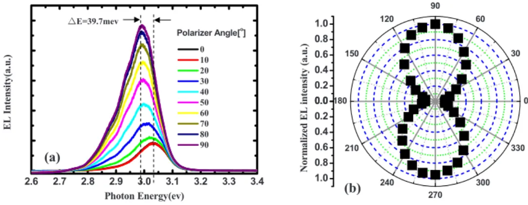
The EL polarization anisotropy12 was observed clearly in the
m-plane LED, as shown in Fig.5. The shift in the peak energy⌬E
and the degree of polarization of the EL intensity of our device were analyzed by rotating a polarizer between the polarization angles 0 and 360°. In Fig.5a, the⌬E is about 39.7 meV between the electric field perpendicular共E⬜兲 to the c-axis component and parallel 共E储兲 to the c-axis component. Our result is close to the theoretical calcu-lation values reported by Kojima et al. using the k · p perturbation theory with similar active layer thickness and In composition.13The shift in the peak energy comes from the splitting of the valence bands caused by the in-plane compressive strain of the MQW, and the energy separation is proportional to the In composition of the active layer. Figure5bshows the angular dependence of the polar-ization ratio under the operation current of 20 mA. The polarpolar-ization ratio is defined as = 共I ⬜ −I 储 兲/共I ⬜ +I 储 兲, where I⬜ is the in-tensity of the E⬜ component and I储 is the intensity of the E储 com-ponent. In Fig.5b, the degree of polarization was estimated to be about 68%, which was about 17% higher than the previous report by Koyama et al.8The degree of polarization in nonpolar LEDs gradu-ally increases with a larger valance band splitting due to the higher In composition as well as higher compressive strain in the active material InGaN.14The large value of the degree of polarization in our m-plane LEDs could be contributed from the higher quality of InGaN epilayers in the MQW because the proper growth condition can prevent the InGaN from serious phase separation on the m-plane GaN surface and can result in higher compressive strain.
In conclusion, we have demonstrated low droop nonpolar m-plane LEDs grown on bulk m-plane GaN substrates and have investigated their EL characteristics. At 22 A/cm2 共20 mA兲 and
330 A/cm2共300 mA兲 under dc operation, the output power and the EQE were 2.4 mW, 4.1% and 29.6 mW, 3.3%, respectively. The EQE only dropped about 18% from maximum at 22 A/cm2to the
operation current density of 330 A/cm2, and the broadening of the
emission linewidth was only about 2 nm. In addition, no droop behavior was observed as increasing the carrier density in the temperature-dependent PL measurements. These results of low droop characteristics could be due to the lack of polarization effects
that enhances the carrier confinement under a high current density operation. The EL polarization anisotropy was observed clearly in the m-plane LED and the degree of polarization was 68%. These results of low droop characteristics shall encourage the development of high performance and high efficiency nonpolar nitride-based semiconductors.
Acknowledgment
These works were supported by the MOE ATU program and in part by the National Science Council of Republic of China in Tai-wan under contract no. NSC-98-3114-M-009-001 and no. NSC-96-2221-E-009-094-MY3.
National Chiao Tung University assisted in meeting the publication costs of this article.
References
1. Y. C. Shen, G. O. Mueller, S. Watanabe, N. F. Gardner, A. Munkholm, and M. R. Krames, Appl. Phys. Lett., 91, 141101共2007兲.
2. M. F. Schubert, S. Chhajed, J. K. Kim, E. F. Schubert, D. D. Koleske, M. H. Crawford, S. R. Lee, A. J. Fischer, G. Thaler, and M. A. Banas, Appl. Phys. Lett.,
91, 231114共2007兲.
3. I. A. Pope, P. M. Smowton, P. Blood, J. D. Thomson, M. J. Kappers, and C. J. Humphrey, Appl. Phys. Lett., 82, 2755共2003兲.
4. M. H. Kim, M. F. Schubert, Q. Dai, J. K. Kim, E. F. Schubert, J. Piprek, and Y. Park, Appl. Phys. Lett., 91, 183507共2007兲.
5. X. Li, X. Ni, J. Lee, M. Wu, Ü. Özgür, H. Morkoç, T. Paskova, G. Mulholland, and K. R. Evans, Appl. Phys. Lett., 95, 121107共2009兲.
6. P. Waltereit, O. Brandt, A. Trampert, H. T. Grahn, J. Menniger, M. Ramsteiner, M. Reiche, and K. H. Ploog, Nature (London), 406, 865共2000兲.
7. Y. J. Sun, O. Brandt, S. Cronenberg, S. Dhar, H. T. Grahn, K. H. Ploog, P. Wal-tereit, and J. S. Speck, Phys. Rev. B, 67, 041306共2003兲.
8. T. Koyama, T. Onuma, H. Masui, A. Chakraborty, B. A. Haskell, S. Keller, U. K. Mishra, H. S. Speck, S. Nakamura, S. P. Denbaars, et al., Appl. Phys. Lett., 89, 091906共2006兲.
9. S. C. Ling, T. C. Wang, J. R. Chen, P. C. Liu, T. S. Ko, B. Y. Chang, T. C. Lu, H. C. Kuo, and S. C. Wang, IEEE Photon. Technol. Lett., 21, 1130共2009兲. 10. M. Funato, M. Ueda, Y. Kawakami, Y. Narukawa, T. Gosugi, M. Takahashi, and T.
Mukai, Jpn. J. Appl. Phys., Part 2, 45, L659共2006兲.
11. N. F. Gardner, G. O. Muller, Y. C. Shen, G. Chen, S. Watanabe, W. Gotz, and M. R. Krames, Appl. Phys. Lett., 91, 243506共2007兲.
12. N. F. Gardner, J. C. Kim, J. J. Wierer, Y. C. Shen, and M. R. Krames, Appl. Phys. Lett., 86, 111101共2005兲.
13. K. Kojima, H. Kamon, M. Funato, and Y. Kawakami, Phys. Status Solidi C, 5, 3038共2008兲.
14. J. Bhattacharyya, S. Ghosh, and H. T. Grahn, Appl. Phys. Lett., 93, 051913共2008兲.
2.6 2.7 2.8 2.9 3.0 3.1 3.2 3.3 3.4 Polarizer Angle[o ] EL Intens ity (a. u .) Photon Energy(ev) 0 10 20 30 40 50 60 70 80 90 △ △E=39.7mev (a) 0.0 0.2 0.4 0.6 0.8 1.0 0 30 60 90 120 150 180 210 240 270 300 330 0.0 0.2 0.4 0.6 0.8 1.0 Norm alized E L intensity (a. u. ) (b)
Figure 5. 共Color online兲 共a兲 Room tem-perature EL spectra with different polar-izer angle, the angle of 0° corresponds to a polarization parallel to a-axis.共b兲 Varia-tion in EL intensity of peak wavelength with angular orientation of the polarizer at 20 mA operation current.
H503
Journal of The Electrochemical Society, 157共5兲 H501-H503 共2010兲 H503
) unless CC License in place (see abstract).
ecsdl.org/site/terms_use
address. Redistribution subject to ECS terms of use (see
140.113.38.11