This content has been downloaded from IOPscience. Please scroll down to see the full text.
Download details:
IP Address: 140.113.38.11
This content was downloaded on 26/04/2014 at 06:25
Please note that terms and conditions apply.
Optical properties of a single free standing nanodiamond
View the table of contents for this issue, or go to the journal homepage for more 2007 J. Phys.: Conf. Ser. 92 012031
(http://iopscience.iop.org/1742-6596/92/1/012031)
Optical properties of a single free standing nanodiamond
Kien Wen Sun and Ching Yao WangDepartment of Applied Chemistry and Institute of Molecular Science, National Chiao Tung University, Hsinchu, 300, Taiwan
E-mail: [email protected]
Abstract. We report the techniques for measuring optical properties of a single nanometer-sized diamond. The electron beam (e-beam) lithography defined coordination markers on a silicon wafer provide us a convenient tool for allocating a single nanodiamond immobilized on the surface. By combining a confocal microscope with the e-beam lithography patterned smart substrate, we are able to measure the Raman and photoluminescence spectra from a single nanodiamond with a size less than 100 nm.
1. Introduction
Bulk diamond is a useful material for its technically important properties including high thermal conductivity, hardness, electrical resistivity and strength. Nanodiamond possesses not only the above properties but also other properties such as special optical properties and magnetoresistivity [1]. It is recently demonstrated that diamonds with a nominal size of 100 nm are capable of producing stable fluorescence from color centers after surface treatment with strong oxidative acids [2]. The fluorescent nanodiamonds could possibly be used as a fluorescent biomarker for in vitro as well as in vivo studies at the single-particle level. In addition, many studies have been motivated by the tremendous technological potential for diamond system composed of nanometer-sized crystalline [3-6]. Although there are some reports on the optical properties of nanodiamonds, however, most of their studies focus on nanodiamonds in cluster or powder form [7-9]. In this work, we report the optical studies from a single free standing nanodiamond on Si under laser excitation at 532 nm using techniques of combining a confocal microscope and an electron-beam (e-beam) patterned smart substrate.
2. Preparation of the single nanodiamond and smart silicon substrates
The nanodiamonds used in this study were all synthesized under high pressure and high temperature (HPHT). The x-ray diffraction and transmission electron microscopy (TEM) analysis reveal that the diamond sample under investigation has crystalline structure. In the experiments, we test two different size nanodiamonds which have average sizes of 90 nm and 35 nm, respectively. Therefore, we expect any changes in the observed optical properties between different nanodiamond samples are most likely due to the size effect.
The powder of 90 nm nanodiamonds is first put in an acid mixture (H2SO4:HNO3 = 3:1) and treated in ultrasonic bath for 30 minutes. It is then diluted and centrifuged in DI water and ethanol mixture to eliminate the large nanodiamond clusters. The solution is placed in an ultrasonic oven for 30 minutes to disperse the nanodiamonds. This ultrasonic bath can break the water molecules and
PHONONS 2007 IOP Publishing
surface can further prevent the clustering of nanoparticles.
Figure 1. SEM image of 2D arrays of 300
nm metal dots defined within an area of 180 μm by 30 μm on Si surface.
Figure 2. Pattern shown in Figure 1 is
repeated several times to cover most of the chip surface.
A Si wafer is diced into 2 cm by 2 cm chips. A pattern of two dimensional arrays of round metal dots with diameter of 300 nm and pitch size of 1.2 μm is defined on the Si chip using e-beam lithography technique within an area of 180 μm by 30 μm. The 2D array pattern is then repeated several times on the same chip. The pitch size of 1μm is determined according to the optical resolution of our confocal microscope at an excitation wavelength of 532 nm. Figures 1 and 2 show the scanning electron microscope) (SEM) images of the patterned substrates. Similar dispersion processes are also applied to the 35 nm nanodiamonds. However, a cross-type coordination marker (as shown in figure 3(a)) is defined using the focused ion beam (FIB) when a single nanodiamond is spotted under SEM.
3. Immobilization of a single nanodiamond
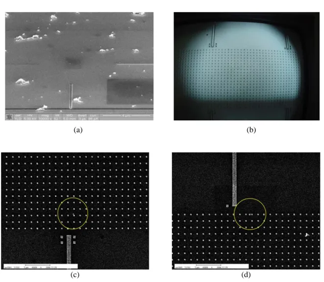
A drop from the diluted nanodiamond solution is spread on the Si surface to anchor the nanodiamond on the surface patterned with coordination markers. The size of markers was properly designed so that they can be clearly seen under optical microscope as shown in figure 3(b). The samples with dispersed nanodiamonds are scanned under the SEM. When a single nanodiamond is found in the SEM images, a corresponding coordinate is assigned. figures 3(c) and 3(d) show the SEM image of the Si surface with an immobilized single nanodiamond near one of the markers and a cluster compose of three nanodiamonds, respectively.
After a single nanodiamond is allocated from the SEM images and a corresponding coordinate is assigned. The laser beam focused through the microscope objective with a spot size of 1 μm is moved to the given coordinate where the single nanodiamond is located. The PL and Raman signals are collected through the same objective and are analyzed by a 0.32 m spectrometer equipped with a liquid nitrogen cooled CCD detector at excitation wavelength of 532 nm.
PHONONS 2007 IOP Publishing
Journal of Physics: Conference Series 92 (2007) 012031 doi:10.1088/1742-6596/92/1/012031
(a) (b)
(c) (d)
Figure 3. (a) A cross-type marker is made with FIB near a single 35 nm nanodiamond (b) optical
image of e-beam defined pattern under confocal microscope (c) SEM image of a single nanodiamond near one of the marker (d) a cluster of three nanodiamonds near one of the marker.
4. Raman and Photoluminescence spectra from a single nanodiamond
For the 90 nm nanodiamond, a single Raman peak due to the sp3 bonding structure in the diamond was detected at the energy of 1328 cm-1 as shown in figure 4(a). This peak is red-shifted by ~ 4 cm-1 in compared to the bulk diamond. The Raman spectrum from the single 35 nm nanodiamond, as shown in figure 4(b), shows a Raman peak at 1325 cm-1. There is also Raman signature due to the sp2 bonding graphite structure at the energy of ~ 1600 cm-1. The decrease of the phonon peak energy as the nanoparticle size is reduced is attributed to the finite-size effect [10]. A broad PL emission centered at about 700 nm, as shown in figure 5, was also observed from both samples at excitation wavelength of 532 nm. The emission at the visible light wavelengths is probably due to the defects, vacancies in the nanodiamonds or the disordered carbon layer covered on the nanodiamond surface [11].
5. Conclusion
In summary, by combining a confocal microscope and an e-beam patterned smart substrate, we are able to study optical properties of a single nanodiamond with a size of less than 100 nm. The Raman peak found in the experiments is red-shifted in compared to the peak found in bulk diamond due to the phonon confinement effect. A broad emission centered at about 700 nm is also observed from the
PHONONS 2007 IOP Publishing
corresponding PL spectra at an excitation wavelength of 532 nm.
(a)
(b)
Figure 4. (color online) Raman Spectra of (a) a single 90 nm nanodiamond and (b) a single 35 nm
nanodiamond
Figure 5. (color online)
Photoluminescence spectra from the single 90 nm nanodiamond.
Acknowledgments
Authors wish to acknowledge support from National Science Council of Taiwan under the Grant No. NSC 095-2112-M-009-046-, NSC 096-2112-M-024-MY3 and the MOE ATU program.
References
[1] Greiner N R, Phillips D S, Johnson and Volk F 1998 Nature (London) 333 440
[2] Yu S J, Kang M W, Chang H C, Chen K M and Yu Y C 2005 J. Am. Chem. Soc. 127 17604
[3] Fu C C, Lee H Y, Chen K, Lim T S, Wu H Y, Lin P K, Wei P K, Tsao P H, Chang H C and Fann W 2007 PNAS 104 727
[4] Yarbrough W A and Sawaoka A B 1990 Carbon 32 665
[5] Davanloo F, Lee T J, You J H and Collins C B 1993 J. Mater. Res. 8 3090 [6] Dorfman V F 1992 Thin Solid Films 212 267
[7] Filik J, Harvey J N, Allan N L and May P W 2006 Phys. Rev. B 74 035423
[8] Zhao F L, Gong Z, Liang S D, Xu N S, Deng S Z, Chen J and Wang H Z 2004 Appl. Phys. Lett. 85 914 [9] Chen J, Deng S Z, Chen J, Yu Z X and Xu N S 1999 Appl. Phys. Lett. 74 3651
[10] Lipp M J, Baonza V G, Evans W J and Lorenzana H E 1997 Phys. Rev. B 56 5978
[11] Hirai H, Terauchi M, Tanaka M and Kondo K 1999 Diamond and Related Materials 8 1703
PHONONS 2007 IOP Publishing
Journal of Physics: Conference Series 92 (2007) 012031 doi:10.1088/1742-6596/92/1/012031