This content has been downloaded from IOPscience. Please scroll down to see the full text.
Download details:
IP Address: 140.113.38.11
This content was downloaded on 28/04/2014 at 14:12
Please note that terms and conditions apply.
Optical and mechanical properties of reactively sputtered silicon dioxide films
View the table of contents for this issue, or go to the journal homepage for more 1996 Semicond. Sci. Technol. 11 1317
(http://iopscience.iop.org/0268-1242/11/9/012)
Optical and mechanical properties of
reactively sputtered silicon dioxide
films
Wen-Fa Wu and Bi-Shiou Chiou
Department of Electronics Engineering and Institute of Electronics, National Chiao Tung University, Hsinchu, Taiwan
Received 22 January 1996, in final form 13 May 1996, accepted for publication 4 June 1996
Abstract. The reactive sputtering method, using an Ar/O2mixture, was applied to
deposit silicon dioxide film. Both x-ray photoemission spectroscopy (XPS) and infrared absorption spectroscopy were employed to evaluate the structure of SiO2
films sputtered at various oxygen percentages. The optical and mechanical properties of SiO2films on glass substrates were investigated. Films prepared at a
higher oxygen content have a higher density and a higher refractive index.
1. Introduction
Silicon dioxide films are extensively used as low-index films in multilayer optical devices [1, 2], passivated and/or protective layers of silicon devices [3], scratch resistant coatings for plastic ophthalmic lenses [4, 5] and so on. Stoichiometry and stability of the films are important during applications. The usual methods employed for forming SiO2 films involve oxidation of silicon at elevated temperatures (T > 900◦C). However, the high-temperature processing results in junction degradation [3]. There are many low-temperature methods used in the preparation of SiO2 films, such as evaporation [1, 2], pyrolytic decomposition [6], plasma enhanced chemical vapor deposition [3, 4, 7], reactive sputtering [6, 8] and radio frequency (rf) magnetron sputtering [9]. Film composition as well as deposition and post-deposition processing conditions strongly affect film microstructure, and, consequently, many of its macroscopic properties. Rao and Mohan [10] found that the stoichiometry of the electron-beam evaporated silicon dioxide film was improved after post-deposition annealing at 250◦C. Valletta et al [8] reported that low substrate temperature, high oxygen pressure, and/or large deposition rate (> 250 ˚A min−1) resulted in increased porosity of reactively sputtered SiO2 films, and, the films contained large amounts of H2O. Sankur and Gunning [11] studied water sorption and intrinsic stress in composite TiO2– SiO2 films and found that annealing reduced the water content of the films. Takahashi et al [12] revealed that the compressive internal stresses of sputtered silicon dioxide films were reduced by use of an Ar/H2 gas mixture instead of the conventional Ar/O2 ones. However, they reported a deficiency of oxygen which led to optical absorption loss at short wavelengths (< 700 nm). The
process conditions, microstructure and ambient effects are interrelated. However, a global optimization of the film properties and deposition conditions is necessary in preparing SiO2 films for applications in a specific field.
In the present study, SiO2 films were prepared by reactive rf magnetron sputtering. The sputtering deposition method is suitable for fabrication of SiO2 films because strong film adhesion onto the substrate is achievable. Previous work by Wu and Chiou [9] indicates that the adhesion strength of SiO2 film to the glass substrate is greater than the strength of the substrate. In this research, the SiO2 films were prepared by reactively sputtering an Si target in an Ar/O2 atmosphere. X-ray photoemission spectroscopy (XPS) was employed to study the chemical bonding states of SiO2 films. Structural evaluation of silicon dioxide films was carried out by Fourier transform infrared spectroscopy. The optical properties, the pull-off strength and scratch adhesion of SiO2 films to the glass substrates are also explored.
2. Experimental details
Silicon dioxide films were prepared by using a commercial rf magnetron sputtering system (Ion Tech, UK). The sputtering target was a 100hot-pressed Si ceramic (99.999% purity) supplied by Cerac, Inc., USA. The substrates employed were Corning 7059 glass and p-type Si (100) wafers. Substrates were placed on a holder above the target with a target-to-holder distance of 50 mm and the holder was rotated at∼ 10 revs/min by a motor to provide good uniformity. However, the film deposition rate is reduced because the substrate was rotated off the plasma region periodically. The vacuum chamber was pumped by a diffusion pump. High-purity Ar (99.999%) and O2
Wen-Fa Wu and Bi-Shiou Chiou
(99.5%) was introduced through a mass flow controller after the vacuum chamber was evacuated to about 2.66×10⁻⁴Pa (2× 10⁻⁶ Torr). The gas pressure was kept at 0.7998 Pa (6× 10⁻³ Torr) and the sputtering power employed was 100 W during deposition.
Film thickness was measured with a stylus surface profiler. An ellipsometer was used to measure refractive indices for films deposited on Si wafers. Chemical binding energy and compositional analyses of the film was performed using an x-ray photoemission spectroscope (XPS, Perkin PHI-590AM SAM/1905 Esca, Massachusetts, USA) with an Mg Kα x-ray source. The microstructure of the film was analysed using a scanning electron microscope (SEM, Hitachi S-4000, Japan). The optical transmittance of the film was measured with an ultraviolet–visible–near-infrared spectrophotometer (Hitachi U-3410, Japan) and a Fourier transform infrared spectrophotometer (Bomen DA 3.002 FTS and MB 100 FT-IR, Canada).
The adhesion strength of the coating was measured by an adhesion pull tester (Sebastian Five Pull Tester, Quad Group, Inc., USA). After the sample surface was cleaned, an epoxy coated stud was attached to the sample surface by a spring mounting clip designed for the stud and the assembly was heated for 60 min at 150◦C to ensure that the stud was bound with the sample. In the tests 0.14100 diameter studs were used and the epoxy binding strength was about 700 kg cm−2. Scratching adhesion testing was performed using commercially available scratch testing equipment (CSEM Revettest, Switzerland) fitted with an acoustic emission detector. In the scratching test a stylus is drawn over the sample surface under a continuously increasing normal force until the coating is detached. The normal force on the indenter causing coating detachment is called the critical load and it represents a comparative value of the coating adhesion. In the study, the loading speed and sample table speed are 100 N min−1 and 10 mm min−1, respectively. The coating detachment was observed using acoustic emission detectors to measure high-frequency vibrations caused by coating detachment. Critical loads indicated were obtained by averaging the values of three to five different scratches. Detailed morphologies of scratch channels were viewed with an optical microscope.
3. Results and discussion
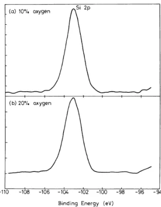
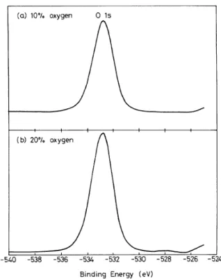
The deposition rate of SiO2 films prepared by reactively sputtering Si target in Ar/O2ambient is∼ 44 ˚A min−1for an oxygen percentage ranging from 10% to 20%. This deposition rate is about one order of magnitude larger than those for SiO2 film sputtered with SiO2 target [9]. The hardness of the SiO2 ceramic target results in a low sputtering yield and consequently a small deposition rate. All the as-sputtered films are amorphous. The film thickness for all specimens in this study was 9000 ˚A. The Si 2p and O 1s XPS spectra of the as-deposited SiO2 films are shown in figures 1 and 2 respectively. The position of the C 1s peak is taken as standard (binding energy= 284.6 eV) to compensate for any charge-induced shifts. The observed binding energies of Si 2p and O 1s levels are ∼103 eV and ∼ 523.7 eV respectively. They
Figure 1. The Si 2p XPS spectra of the as-deposited SiO2
films prepared at (a) 10% O2and (b) 20% O2.
Table 1. XPS compositional analyses of SiO2films
prepared at 10% and 20% oxygen. O2/O2+ Ar Atomic concentration (%)
(%) XO XSi XO/XSi
10 65.68 34.32 1.914
20 69.70 30.30 2.3
agree well with the binding energies of SiO2 reported in the literature [13]. Table 1 presents the corresponding XPS compositional analyses of SiO2 films. Here compositional analyses are accomplished by dividing the peak areas by their respective atomic sensitivity factors thus obtaining atomic per cent concentrations. The O/Si atomic ratio of the film is close to that of the nominal composition. Nevertheless, the O/Si atomic ratio of the SiO2 film prepared at 20% oxygen is larger than that of the SiO2 film prepared at 10% oxygen. Figure 3 illustrates SEM micrographs of SiO2 films prepared at 10% and 20% oxygen.
The structures of silicon dioxide films were evaluated using Fourier transform infrared spectroscopy. Figure 4 shows the infrared spectra measured over the wave number range from 1400 to 600 cm−1 for SiO2 films prepared at various oxygen percentages. It has been reported that the wave numbers corresponding to the Si–O vibrational band are 968, 1035 and 1078 cm−1 for SiO, Si2O3 and SiO2 respectively [10]. As shown in figure 4, the positions of the Si–O vibrational band of rf sputtered SiO2 films are 1080± 5 and 840 cm−1. They agree well with the band
Figure 2. The O 1s XPS spectra of the as-deposited SiO2
films prepared at (a) 10% O2and (b) 20% O2.
positions of SiO2reported in the literature [6, 8, 10]. Pliskin and Lehman [6] have shown that the positions and half-widths of the Si–O vibrational bands near 1090 cm−1 are strongly influenced by the bonding character, stoichiometry, density and porosity of the films. For example, they show that the position of the 1090 cm−1 band shifts to larger wave number and the corresponding band width decreases as pyrolytic SiO2films are densified. As shown in figure 4, the band width of the Si–O vibrational band near 1080 cm−1 is broader for SiO2 film prepared at 10% oxygen than that of SiO2film prepared at 20% oxygen. This implies that the film prepared at 10% oxygen is more porous than the film prepared at 20% oxygen.
The corresponding spectra of SiO2films in the spectral region where adsorbed water could be found are shown in figure 5. The intensity of the absorption band near 3650 cm−1 due to hydrogen bonded hydroxyl groups and adsorbed water is indicative of the quantity of surface hydroxyl groups and porosity of the oxides. As exhibited in figure 5, the intensity of the infrared absorption near 3650 cm−1 decreases as the oxygen percentage increases. It agrees well with the result in figure 4. As shown in table 2, ellipsometry measurements of the refractive index give values of 1.453 ± 0.003 and 1.460 ± 0.004 for SiO2 films prepared at 10% and 20% oxygen respectively. The refractive index of the film is influenced by both its density and stoichiometry. Films deposited with less oxygen but the same density will have a higher refractive index due to the larger index of Si-rich films. The effects of density and stoichiometry can compete to some extent in their effect on refractive index. However, films in this study are close to stoichiometric and the major effect will be due to density.
Figure 3. SEM micrographs of SiO2films prepared at
(a) 10% O2and (b) 20% O2.
Figure 4. Infrared spectra for SiO2films prepared at
various oxygen percentages.
The greater the density, the larger is the refractive index. Figure 6 shows the transmittance of SiO2films prepared at various oxygen percentages. As indicated in figure 6, the transmittance of the film prepared at 20% oxygen is marginally larger than that of the film prepared at 10% oxygen. The transmittance of film prepared at 20% oxygen is larger than that of the glass substrate. The spectral characteristics of the film prepared at 10% oxygen are more oscillatory than those of the film prepared at 20%
Wen-Fa Wu and Bi-Shiou Chiou
Table 2. Properties of SiO2films deposited on glass substrates at a sputtering pressure of 6×10⁻³Torr.
Pull-off strength Critical load Gas ambient Refractive index (kg cm−1) (N)
90% Ar + 10% O2 1.453±0.003 531 11.0±2.0
80% Ar + 20% O2 1.460±0.004 486† 13.8±3.7
†Failure occurred within glass substrates.
Figure 5. Infrared spectra for SiO2films prepared at
various oxygen percentages. Arrows indicate the
absorption band due to hydrogen bonded hydroxyl groups and adsorbed water.
Figure 6. Transmittance of SiO2films prepared at various
oxygen percentages.
oxygen, although this is not shown clearly in figure 6 on the transmission versus wavelength plot. This is attributed to the smaller refractive index of the film prepared at a lower oxygen percentage (10%). The refractive indices of the Corning 7059 glass substrate, the 10% O2sputtered film and the 20% O2 sputtered film are 1.523, 1.453 and 1.460 respectively. The 10% O2 sputtered film on glass has a larger refractive index mismatch than the 20% O2sputtered one and would contribute to more oscillatory transmission spectra.
Figure 7. Acoustic emission curves for SiO2films prepared
at (a) 10% O2and (b) 20% O2.
Table 2 summarizes the results concerning the adhesion properties of SiO2 films on glass substrates. As indicated in table 2, a high pull-off strength (> 486 kg cm−2) is obtained for films deposited on glass substrates. For the 20% O2 sputtered film, failure occurred within the glass substrate and did not occur at the interface between the film and the glass substrate. This implies that the bonding between the SiO2 film and the glass substrate is excellent.
Figure 7 shows acoustic emission curves for films prepared at 10% and 20% oxygen. The critical loads are 11.0 ± 2.0 N and 13.8 ± 3.7 N for the 10% O2 and 20% O2 sputtered films, respectively. No apparent difference is observed between the 10% O2 and 20% O2 sputtered film. The critical load measured by a scratch test technique can be thought of as the adhesion strength of the film on the substrate when films are subjected to wearing and/or abrasion. The reactively sputtered SiO2 film with an Si target is more scratch resistant than those sputtered with
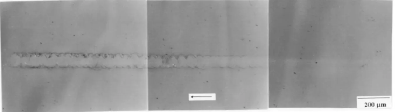
Figure 8. A typical optical micrograph of the scratch channel for the SiO2film.
an SiO2 target. The critical loads are 13.8 ± 3.7 N and 8.0 ± 2.0 N for films prepared with Si and SiO2 targets respectively [9].
Figure 8 shows a typical optical micrograph of the scratch channel. The arrow indicates the scratch direction. Roughly semicircular arcs appear in front of the scratch channel. The cracking is more intense and is coupled with a loss of adhesion at higher loads. However, the film is not removed as its coherence is high.
4. Conclusions
Silicon dioxide films were prepared by reactively sputtering an Si target in an oxygen-containing ambient. The deposition rate is ∼ 44 ˚A min−1 for an oxygen percentage ranging from 10% to 20%. Both the XPS and infrared spectra confirm the formation of SiO2 compound. However, compositional analyses indicate an increase in O/Si atomic ratio with the increase of oxygen percentage in the sputtering gas. In addition, the absorption band near 3650 cm−1suggests the existence of surface hydroxyl groups and porosity. Films prepared at a higher oxygen content have a higher density and a greater refractive index. In addition, reactively sputtered SiO2films with an Si target are more scratch resistant than films sputtered with an SiO2 target.
Acknowledgment
This work is supported by the Chung-Shan Institute of Science and Technology (contract no CS 83-0210-D-009-001) and partly supported by the National Science Council of Taiwan, Republic of China (contract no NSC 82-0417-E009-395).
References
[1] Welsch E, Walther H G, Sch¨afer D, Wolf R and M¨uller H 1988 Thin Solid Films 156 1
[2] Stone J and Stulz L W 1990 Appl. Opt. 29 583 [3] Robles S, Yieh E and Nguyen B C 1995 J. Electrochem.
Soc. 142 580
[4] Klug W, Schneider R and Z¨oller A 1990 Proc. SPIE 1323 88
[5] Masso J D 1985 Proc. SPIE 601 60
[6] Pliskin W A and Lehman H S 1965 J. Electrochem. Soc. 112 1013
[7] Chanana R K, Dwivedi R and Srivastava S K 1993
Solid-State Electron. 36 1021
[8] Valletta R M, Perri J A and Riseman J 1966 Electrochem.
Technol. 4 402
[9] Wu W F and Chiou B S 1996 Appl. Surf. Sci. at press [10] Rao K N and Mohan S 1989 Thin Solid Films 170 179 [11] Sankur H and Gunning W 1989 J. Appl. Phys. 66 807 [12] Takahashi H, Nagata H, Kataoka H and Takai H 1994
J. Appl. Phys. 75 2667