WP-(16)-10
NUMERICAL ANALYSIS OF TWO-DIMENSIONAL PHOTONIC
CRYSTAL DIRECTIONAL COUPLERS
Kuan-Ming Chen, Yen-Cheng
Lu,
Tzu-Hao Wang, Jyh Yang Wang, Homg-Shyang Chen,
Yean-Woei Kiang, Hua-Kuang Liu, and C. C. Yang
Graduate Institute of Electro-Optical Engineering, Graduate Institute
of
Communication
Engineering, Graduate Institute
of
Electronics Engineering, and Department
of
Electrical
Engineering, National Taiwan University,
1,
Roosevelt Road, Section
4, Taipei, Taiwan, R.O.C.
(phone) 886-2-23657624 (fax) 886-2-23652637 (e-mail) [email protected]
Abstract-2-D photonic crystal directional couplers of various line defect patterns were numerically analyzed with the plane-wave and FDTD mefhods for showing the coupling iengfh dependence and other propagation and coupling characteristics.
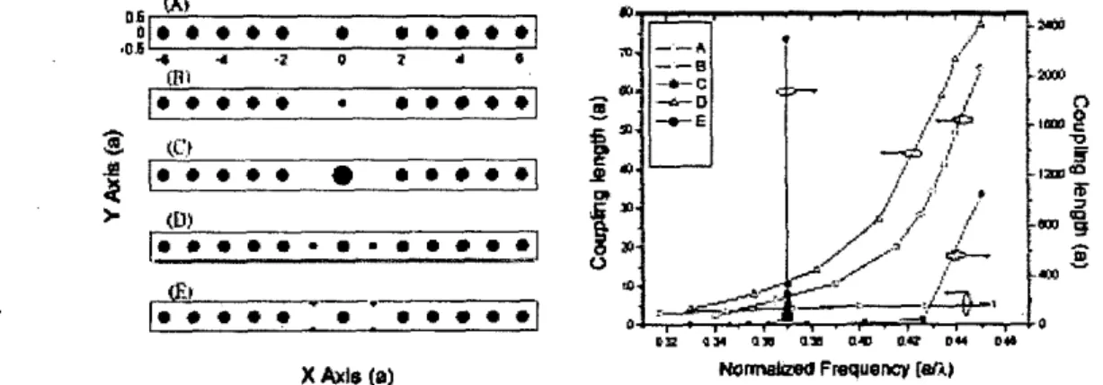
In this paper, we numerically study the coupling behaviors of 2-D photonic crystal directional couplers. We investigated the dependencies of coupling phenomena on the variation of line defect pattern. In other words, we varied the cell structures between the two line-defect waveguides for controlling the coupling phenomena. The plane-wave method was used for evaluating the band structures and the mode field patterns. The finite-difference time-domain (FDTD) technique was used for confirming the accuracy of the plane-wave-method computations ind evaluating the wave field evolution during the coupling process. The 2-D photonic crystals of both dielectric-rod and air-hole structures were considered. We consider the photonic crystals of dielectric-rod arrays first. Fig. 1 shows five line defect patterns of a square photonic crystal structure ( d a = 0.18, d = rod radius and a = crystal period) as: (A) two line defects with one unit cell apart to form a directional coupler; (B) two line defects with the radius of the rods in between reduced to d'/a = 0.1; (C) two line defects with the radius of the rods in between enlarged to d"/a = 0.3; (D) two line defects of reduced rods as
d'/a = 0.1; .and (E) two line defects with reduced rods shifted by one-half unit cell in the propagation direction (the y axis), The dielectric constant of the rod material is 11.4. Typically, the coupling length of a directional coupler of two super-modes is defined as x divided by the difference of propagation constants of the two modes (one even mode and one odd mode). Because there are four super-modes in the directional coupler C, we define the coupling length based on the even and odd mode pair of the lower frequency. With the definition of this manner for the couplers of four super-modes, we summarize the results of coupling length for various directional couplers in Fig. 1 as various curves in Fig. 2. Except the situation of degeneracy in case C, coupling length generally increases with frequency. First, the directional coupler with two standard line defects in case A
shows tens of unit cells for coupling length. When the central rod size is reduced, the coupling length is
tremendously decreased down to a few unit cells. On the other hand, when the central rod is enlarged (case C), degeneracy occurs near 0.37 in normalized frequency, at which the coupling length shows a peak. Then, when small rods are placed at the line defects
as
case D, coupling length is enhanced, compared with the standard line defects structure (case A).In
particular, when the small rods of the line defects are shifted by one-half unit cell (case E), coupling length is tremendously increased at the high frequency end.x
&dB ( 0 )Fig. 1 Various photonic crystal directional couplers.
N o wFrequeBcy leW
Fig. 2 Coupling lengths as functions of frequency.
0-7803-7766-4/03/117.00 02003 IEEE