Electron mobility in Ge and strained- Si channel ultrathin-body metal-oxide semi
conductor field-effect transistors
Tony Low, M. F. Li, Chen Shen, Yee-Chia Yeo, Y. T. Hou, Chunxiang Zhu, Albert Chin, and D. L. Kwong
Citation: Applied Physics Letters 85, 2402 (2004); doi: 10.1063/1.1788888 View online: http://dx.doi.org/10.1063/1.1788888
View Table of Contents: http://scitation.aip.org/content/aip/journal/apl/85/12?ver=pdfcov
Published by the AIP Publishing
Articles you may be interested in
Improvement of subthreshold swing of n -channel transistor by uniaxial tensile stress due to a quantum mechanical mechanism instead of physical thinning
Appl. Phys. Lett. 94, 173503 (2009); 10.1063/1.3125248
Drive current enhancement in p -type metal–oxide–semiconductor field-effect transistors under shear uniaxial stress
Appl. Phys. Lett. 85, 6188 (2004); 10.1063/1.1841452
Evidence of Si SiGe heterojunction roughness scattering
Appl. Phys. Lett. 85, 4947 (2004); 10.1063/1.1828224
Monte Carlo based analysis of intermodulation distortion behavior in GaN–Al x Ga 1x N high electron mobility transistors for microwave applications
J. Appl. Phys. 90, 3030 (2001); 10.1063/1.1390495
Surface roughness at the Si–SiO 2 interfaces in fully depleted silicon-on-insulator inversion layers
J. Appl. Phys. 86, 6854 (1999); 10.1063/1.371763
This article is copyrighted as indicated in the article. Reuse of AIP content is subject to the terms at: http://scitation.aip.org/termsconditions. Downloaded to IP: 140.113.38.11 On: Thu, 01 May 2014 04:12:10
Electron mobility in Ge and strained-Si channel ultrathin-body metal-oxide
semi conductor field-effect transistors
Tony Low, M. F. Li,a)Chen Shen, Yee-Chia Yeo, Y. T. Hou, and Chunxiang Zhu
Silicon Nano Device Laboratory, Department of Electrical and Computer Engineering National University of Singapore and Institute of Microelectronics, Singapore 119260, Singapore
Albert Chin
Department of Electronics Engineering, National Chiao Tung University, Taiwan
D. L. Kwong
Department of Electrical and Computer Engineering, University of Texas, Austin, Texas 78752 (Received 26 February 2004; accepted 2 July 2004)
Electron mobility in strained silicon and various surface oriented germanium ultrathin-body(UTB) metal-oxide semiconductor field-effect transistors (MOSFETs) with sub-10-nm-body thickness are systematically studied. For biaxial tensile strained-Si UTB MOSFETs, strain effects offer mobility enhancement down to a body thickness of 3 nm, below which strong quantum confinement effect renders further valley splitting via application of strain redundant. For Ge channel UTB MOSFETs, electron mobility is found to be highly dependent on surface orientation. Ge具100典 and Ge具110典 surfaces have low quantization mass that leads to a lower mobility than that of Si in aggressively scaled UTB MOSFETs. © 2004 American Institute of Physics. [DOI: 10.1063/1.1788888]
Ultrathin-body (UTB) transistors with sub-10-nm-body thickness Tbody is a promising candidate for device scaling
into the sub-30-nm gate length LGregime. However, degra-dation of electron mobility in UTB devices with sub-10-nm Tbodywas found experimentally.
1,2
Degration of mobility also leads to reduce current drivability in the linear regime3 de-spite the improved gate inversion layer capacitive coupling with reduced body scaling.3Of particular concern is current drivability under high drain biases for decananometer chan-nel length devices. With regard to this, Lundstrom4 has pointed out, via a phenomenological approach, that the trans-port in decananometer metal-oxide semiconductor field-effect transistor (MOSFETs) is essentially source limited; hence the mobility at high vertical surface field, which em-bodies the effective scattering rate in the vicinity of the source, remains relevant. In addition, recent reports on ag-gressively scaled UTB devices have highlighted the impor-tance of the interfacial perturbation attributed to the rough-ness of the Si/ SiO2 surface,
2,5
which is found to strongly limit the carrier mobility. For enhanced device performance, channel materials such as Ge and strained-Si (formed di-rectly on insulator without a relaxed SiGe buffer layer) may be employed in UTB transistor.6,7Nevertheless, there is little work on their potential advantages. Little is also known about the carrier mobility in these UTB devices with ad-vanced channel materials. In this letter, we perform a mod-eling study of the electron mobility in UTB transistor with sub-10-nm-body thicknesses employing strained-Si and vari-ous surface orientations of Ge as the channel material. A calibrated physical model that takes the effect of scattering due to optical phonons, acoustic phonons, surface roughness, and interface states into account is used.
Electronic structures for the two-dimensional electron gas are obtained by solving the coupled Schrödinger–Poisson equation self-consistently within the envelope function based
effective mass framework according to Stern et al.8 Impor-tant bandstructure parameters such as the conduction valleys energy minima and their longitudinal and transverse masses used are obtained from Fischetti et al.9A unitary transforma-tion is employed8,10to obtain the transport masses along the device coordinates for devices with various crystal orienta-tions. The 2D density-of-states mass is preserved after the transformation in our context of low longitudinal field. The scattering matrix elements due to acoustic phonons (AP), optical phonons(OP), surface roughness (SR), and interface states(DIT) related scattering are then systematically formu-lated. The model for phonon spectrum in the bulk semicon-ductors are adapted from Jacoboni et al.11,12where the matrix elements of the electron-phonon interaction are considered in accordance with Price11,13,14 Intravalley acoustic phonon
(AP) with an effective isotropic deformation potential11,15,16
intravalley optical phonon(OP) for L valleys11,12 and inter-valley phonons constraint within the selection rules for f and g type processes11 are accounted for. Dynamic screening of phonons is disregarded.17 Surface roughness(SR) scattering was conventionally treated by accounting for the localized perturbation potential due to variations of interface positions according to Ando’s.18–20The perturbation Hamiltonian in-duced by energy level fluctuations has been obtained21,22for a rectangular quantum well potential, but this approach may not be accurate for the treatment of surface roughness in UTB devices. Issues also remain about the accurate treat-ment of perturbation potential due to change in charge den-sity induced by SR. Consequently, we employed a phenom-enological treatment as outlined by Gamiz.23 The autocorrelation function of the asperities is assumed to be Gaussian. Intersubband transitions are left unscreened and the dielectric matrix is expressed according to Ref. 14 and in the quantum size limit when applicable, else it is left un-screened. Interface state (DIT) induced scattering potential according to Stern et al.8based on a perturbative approach is employed. By imposing appropriate boundary conditions, the scattering potential in all regions of interest can be obtained
a)Electronic mail: [email protected]
APPLIED PHYSICS LETTERS VOLUME 85, NUMBER 12 20 SEPTEMBER 2004
0003-6951/2004/85(12)/2402/3/$22.00 2402 © 2004 American Institute of Physics
This article is copyrighted as indicated in the article. Reuse of AIP content is subject to the terms at: http://scitation.aip.org/termsconditions. Downloaded to IP: 140.113.38.11 On: Thu, 01 May 2014 04:12:10
using the Nystrom method.15 The scattering rate can be ob-tained by the Fermi Golden Rule. We then obob-tained the nu-merical solutions of the scattering time to the Boltzmann equation in the Ohmic regime by embracing the relaxation time approximation and imposing the appropriate scattering condition under detailed balance condition at equilibriums.15,16
Our physical model is calibrated using experimental Si mobility data,24showing good agreement[Fig. 1(a)]. An ef-fective acoustic deformation potential of 15 eV14,15 was used. As current processing technology is still unable to yield a reliable set of mobility data for Ge MOSFETs, a deforma-tion potential of 15 eV for acoustic phonon intravalley pro-cess within valleys is assumed, yielding a reasonable two times mobility compared to Si counterpart25,26 as shown in Fig. 1(a). A SR autocorrelation function with root mean square⌬=4 Å and correlation length l=10 Å is assumed for Si and Ge7surfaces. These technologically dependent param-eters are assumed to apply to UTB transistor technology. A conservative interface states density of 1⫻1011cm−2 for
each of the front and back interfaces is assumed. Our UTB device has a gate dielectric with an EOT of 1 nm, a metal gate electrode (which provides efficient charge screening), and back oxide thickness of 50 nm. The mobility for a 2 nm TbodySi UTB MOSFET is calculated as shown in Fig.
1(a). It is observed that its electron mobility at high surface field does not exhibit the same dependency on effective field as the bulk universal mobility. Perturbation Hamiltonian due to SR HSRas obtained to first order approximation is:
HSR共z,r兲 ⬵
q0关V共z,⌬m兲 − V共z,0兲兴⌬共r兲
⌬m
, 共1兲
where the coordinates z(perpendicular to Si/SiO2 interface,
measured from back oxide interface) and r (vector in the plane of the Si/ SiO2interface) are employed.⌬共r兲 is a
func-tion which effectively describes the sum of SR at the two interfaces and⌬mis the statistical mean of the SR. V共z,⌬m兲 is the electrostatic potential with a surface perturbation of
⌬m, which is also solved self-consistently accounting for the finite body thickness fluctuation⌬m. However, at large body thickness, one obtains
Tbodylim →⬁HSR⬵ q0 V共z + ⌬m,0兲 − V共z,0兲 ⌬m ⌬共r兲 ⬵ q0 V z⌬共r兲, 共2兲
where HSR is now proportional to the surface field V
Ⲑ
dz, accounting for the usual dependence of surface roughness limited mobility on effective field ⬃Feff2 in the bulkSi MOSFET. When Tbodyin the order of SR, deviation from
usual electric field dependency is captured by HSRin Eq.(1).
The electron mobility as a function of Tbodyis calculated
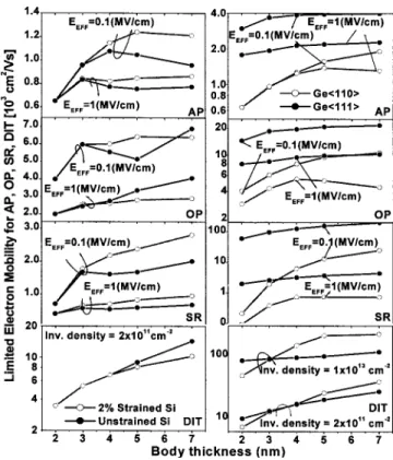
for strained Si (with biaxial tensile strain of 2%, consider-ably larger based on current technology) and Ge with differ-ent surface oridiffer-entations, as shown in Fig. 1(b). At high effec-tive field of 1 MV/ cm, SR induced scattering dominates the effective mobility. The limited mobilities due to AP, OP, SR, and DIT are also calculated as a function of Tbody(Fig. 2), clearly indicating the dominance of SR limited mobility at an effective field of 1 MV/ cm. The application of strain is found to lose its effectiveness at⬃3 nm of Tbodyas shown in the inset of Fig. 1(c). This is because, at small Tbody, strong
quantum confinement lifts the⌬4 valleys much beyond that
of the high mobility ⌬2 valleys, rendering further valley splitting via application of strain redundant. It has been as-sumed that the SR spectrum function in strained or
un-FIG. 1.(a) Calibration of our theoretical low-field
mo-bility model with experimental results for Si(Ref. 24). Theoretical calculated mobility for a 2 nm TbodySi
UTB MOSFET is also shown. Screening for SR scat-tering is accounted.(b) Electron mobility for various
advanced channel UTB transistors as function of body thickness. Si channel is oriented in [010] direction. Ge具100典 is oriented along 关010兴 channel direction, Ge具110典 at 关11¯0兴 and Ge具111典 is isotropic. We ignored the neighboring⌬ valley in this work. (c) replots the mobility curve in linear scale for the Si具100典 curve in the main figure. A peak is clearly shown, in good agree-ment with the experiagree-ment(See Refs. 1 and 2). A mobil-ity curve for strained Si具100典 is also plotted for comparison.
FIG. 2. Limited low field mobilities for strained Si and Ge UTB transistor, respectively. Acoustic phonons, optical phonons, SR, and interface charge limited mobilities are all systematically explored. All limited mobilities are plotted at constant effective field of 0.1 MV/ cm(threshold condition) and 1 MV/ cm(high inversion condition) except for interface charge limited mobility plotted at a constant electron density criterion.
Appl. Phys. Lett., Vol. 85, No. 12, 20 September 2004 Lowet al. 2403
This article is copyrighted as indicated in the article. Reuse of AIP content is subject to the terms at: http://scitation.aip.org/termsconditions. Downloaded to IP: 140.113.38.11 On: Thu, 01 May 2014 04:12:10
strained Si devices are the same. Of particular interest is the choice of channel surface orientations for optimum device performance. Figure 1(b) compares the total effective mobil-ity of Ge and Si channel UTB devices with Tbody of
sub-10-nm. Interestingly, while the electron mobility in bulks Ge is higher than that in bulk Si, Ge具110典 and Ge具100典 UTB devices have lower mobility than Si具100典 at Tbody below
3 nm. Ge具111典 shows better mobility than Si具100典 at all body thicknesses. Generally, it is observed that at sufficiently thin Tbody, the electron mobility begins to degrade. The onset
and amount of this degradation differs for the various orien-tations.
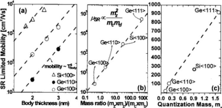
Sakaki et al.22 has established the SR limited mobility with a Tbodyto a power of 6 dependency for the of quantum
well.22 Uchida et al. have also experimentally verified this dependency for Si UTB with small Tbody at low inversion charge condition.2Our model predicts a similar dependency on Tbodyfor the SR mobility at a low constant surface field of
0.1 MV/ cm, as shown in Fig. 3(a). In addition, the SR lim-ited mobility for UTB with small Tbodyat low constant
sur-face field approximately follows a mass ratio relationship as elucidated in Fig. 3(b). However, since SR scattering domi-nates in the high effective surface field regime, it is of para-mount importance to examine their mobility in this regime, where SR induced charge perturbation will contribute addi-tional SR perturbation potential. Figure 3(c) plots the elec-tron mobility at high effective surface field as a function of quantization mass for the various channel materials. A gen-eral trend of decreasing electron mobility with reduced quan-tization mass can be observed. This can be phenomenologi-cally explained by the effect of quantization mass on the screening of potential. A larger quantization mass causes the carriers to be nearer to the interface resulting in more effi-cient potential screening. This reduces the overall SR pertur-bation potential. Conversely, a small quantization mass will render very sensitive to the SR condition.
In summary, the electron mobility of UTB MOSFETs with sub-10-nm Tbody and advanced channel materials are
systematically studied. At small Tbody, Ge具100典 and Ge具110典
suffer large mobility degradation due to their very low quan-tization masses, resulting in high susceptibility to SR scatter-ing. Ge具111典 with its large quantization mass and low den-sity of state mass is highly desirable for high mobility in the ultrathin-body regime.
This work is supported by the Singapore A*STAR R263-000-267-305 and IME/03–450002 JML/SOI Grant. We
gratefully acknowledge useful discussions with D. Esseni on Coulomb scattering. We appreciate useful discussions with M. V. Fischetti and D. K. Ferry pertaining to their published literatures. We also thank S. Takagi for providing the experi-mental data from his classic paper.
1
K. Uchida, J. Koga, R. Ohba, T. Numata, and S. Takagi, Tech. Dig. - Int. Electron Devices Meet. 2001, 633(2001).
2
K. Uchida, H. Watanabe, A. Kinoshita, J. Koga, T. Numata, and S. Takagi, Tech. Dig. - Int. Electron Devices Meet. 2002, 47(2002).
3
See Ref. 1. Figure 10 shows the enhanced inversion layer capacitances with body scaling from 25 to 7 nm. Figure 13 shows the degradation of current drivability in linear regime, attributing mainly to degradation of low-field mobility.
4
M. S. Lundstrom, IEEE Electron Device Lett. 22, 293(2001).
5
Z. Ren, P. M. Solomon, T. Kanarsky, B. Doris, O. Dokumaci, P. Pldigies, R. A. Roy, E. C. Jones, M. Leong, R. J. Miller, W. Haensch, and H. S. Wong, Tech. Dig. - Int. Electron Devices Meet. 2002, 51(2002).
6
K. Rim, K. Chan, L. Shi, D. Boyd, J. Ott, N. Klymko, F. Cardone, L. Tai, S. Koester, M. Cobb, D. Canaperi, B. To, E. Duch, I. Babich, R. Carruth-ers, P. SaundCarruth-ers, G. Walker, Y. Zhang, M. Steen, and M. Leong, Tech. Dig. - Int. Electron Devices Meet. 2003, 49(2003).
7
S. Nakaharai, T. Tezuka, N. Sugiyama, Y. Moriyama, and S. Takagi, Appl. Phys. Lett. 83, 3516(2003).
8
F. Stem and W. E. Howard, Phys. Rev. 163, 816(1967).
9
M. V. Fischetti and S. E. Laux, J. Appl. Phys. 80, 2234(1996), see Figs.
1 and 4.
10
A. Rahman, A. Ghosh, and M. Lundstrom, Tech. Dig. - Int. Electron Devices Meet. 2003, 471(2003).
11
C. Jacoboni and L. Reggiani, Rev. Mod. Phys. 55, 645(1983).
12
C. Jacoboni, F. Nava, C. Canali, and G. Ottaviani, Phys. Rev. B 24, 1014
(1981).
13
P. J. Price, Ann. Phys.(San Diego) 133, 217 (1981).
14
C. Jungemann, A. Emunds, and W. L. Engl, Solid-State Electron. 36, 1529(1993).
15
D. Esseni and A. Abramo, IEEE Trans. Electron Devices 50, 1665(2003).
16
D. Esseni, A. Abramo, L. Selmi and E. Sangiorgi, Tech. Dig. - Int. Elec-tron Devices Meet. 2002, p 719(2002).
17
M. V. Fischetti, and S. E. Laux, Phys. Rev. B 48, 2244(1993).
18
T. Ando, J. Phys. Soc. Jpn. 43, 1616(1977).
19
T. Ando, A. B. Fowler, and F. Stern, Rev. Mod. Phys. 54, 437(1982).
20
D. Esseni, IEEE Trans. Electron Devices 51, 394(2004).
21
C. Y. Mou and T. M. Hong, Phys. Rev. B 61, 12612(2000).
22
H. Sakaki, T. Noda, K. Hirakawa, M. Tanaka, and T. Matsusue, Appl. Phys. Lett. 51, 1934(1987).
23
F. Gamiz, J. B. Roldan, J. A. Lopez-Villanueva, P. Cartujo-Cassinello, and J. E. Carceller, J. Appl. Phys. 86, 6854(1999).
24
S. Takagi, A. Toriumi, M. Iwase, and H. Tango, IEEE Trans. Electron Devices 41, 2357(1994).
25
C. M. Ransom, T. N. Jackson, and J. F. DeGelormo, IEEE Trans. Electron Devices 38, 2695(1991).
26
C. H. Huang, D. S. Yu, A. Chin, C. H. Wu, W. J. Chen, C. Zhu, M. F. Li, B. J. Cho, and D. L. Kwong, Tech. Dig. - Int. Electron Devices Meet.
2003, 319(2003).
FIG. 3. (a) SR limited mobility plotted at
ef-fective surface field of 0.1 MV/ cm, exhibit-ing approximately the Tbody
6
dependency, (b) surface roughness limited mobility at effective surface field of 0.1 MV/ cm as function of mass ratio as expressed in inset, with Tbody
= 2 nm under same SR condition.(c) Electron mobility as function of quantization mass mz.
Simulated at Tbody= 2 nm and Eeff
= 1 MV/ cm. High quantization mass mz, is
beneficial for aggressively scaled UTB device.
2404 Appl. Phys. Lett., Vol. 85, No. 12, 20 September 2004 Lowet al.
This article is copyrighted as indicated in the article. Reuse of AIP content is subject to the terms at: http://scitation.aip.org/termsconditions. Downloaded to IP: 140.113.38.11 On: Thu, 01 May 2014 04:12:10