UEOA, o., TAKAGI, H., and KANO, e.: 'A new vertical power MOSFET structure with extremely reduced on-resistance', IEEE Trans., 1985, ED-32, pp. 2-6
BALIGA, B. J . : 'Self-aligned UMOSFET's with a specific on- resistance of I m n . cm", IEEE Trans., 1987, ED-34, pp. 2329- 2334
CHANG, H . - R . : 'Numerical and experimental comparison of 60 V vertical double-diffused MOSFETs and MOSFETs with a trench- gate structure', Solid-State Electron., 1989. 32, pp. 241-25 I
MATSUMOTO, s., OHNO, T., and izuMi, K : 'Ultralow specific on resist- ance UMOSFET with trench contacts for source and body regions realised by selfaligned process', Electron. Lett., 1991, 27,
pp. 1640-1642
SYAU, T., BALIGA, B I., and HAMAKER, R. w.: 'Reactive ion etching of silicon trenches using SF,/O, gas mixtures', J. Electrochem. Soc.,
1991,138, pp. 3076-3081
CHANG, H.-K., BLACK, R. 0.. TEMPLE, V. A. K., TANTRAPOKN, W., and
I M A G E INTERPOLATION BY ANALOGUE
CIRCUIT
H.-C. Hsieh
a n dW.-T.
C h a n gIndexing terms ' Image processing. Analogue computers, Circuit desion
for all (i mod M ) # 0. With this, a set of equations are obtained
i = 1
i = N - 1 i mod M = 0
i
U , - , - 4v,-,+
6 4 - 4 v j + ]+
u , + ~ = 0 otherwise These equations can be rewritten as- 21;,
+
50, - 40,+
U 3 = 0 -2u,+
5 u N - , - 4v,-,+
u , - ~ = 0 U , = U L (3) 2(U, - V i )+
q u 2
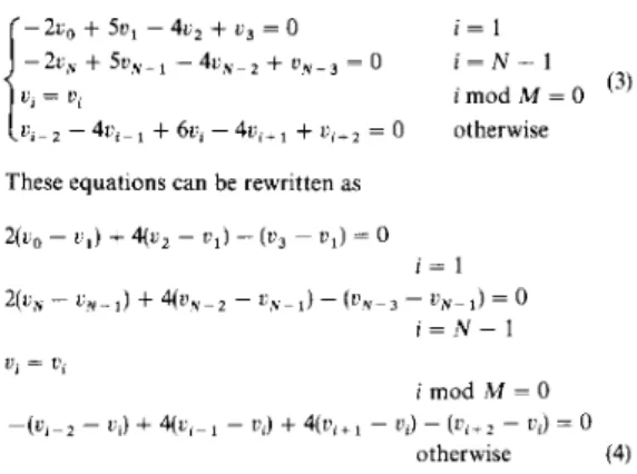
- V i ) - ( U j - U ] ) = 0 2(UN-U,w-i)+qU,.-2 - U , w ~ ] ) - ( L ' ~ i 3 - v , ~ 1 ) = o i = 1 i = N - 1 i mod M = 0 otherwise (4)These equations can he transformed to the node equations of a resistive circuit. Therefore, a resistive circuit can be con- structed to solve the desired sequence. The graph of this circuit is shown in Fig. 1. The connection of this circuit is regular except at the two ends. The labels in Fig. 1 indicate the conductance values of the connecting resistors. In the implementation, voltage inverters can be used for negative conductances.
U , = U ,
-(U,-2 - U,)
+
4(U,-, - U , )+
4(t',+, - U , ) - ( C L t 2 - U j ) = 04 I 4 2 "N
An analogue computation circuit is proposed for image inter- polation. This circuit is designed to maximise the smoothness of the interpolated data. With this circuit, high speed inter- polation can be easily achieved.
Introduction: Interpolation is widely used in image processing. Various methods have been proposed [l]. However, most of those methods are limited in speed and are not efficient for real-time applications. Recently, high speed interpolation has become desirable in many real-time applications such as visual communication, advanced television systems, etc. For
high speed computation, analogue computation has been an attractive approach [2, 31. In this Letter, an analogue compu- tation circuit is proposed for image interpolation.
In classical interpolation methods, lowpass filtering is com- monly used for smoothing the interpolated data. In the pro- posed method, instead of lowpass filtering, an optimisation process is used to maximise the smoothness of the inter- polated data. The advantage of maximising the global smoothness is that a set of simultaneous equations can be derived. This set of equations can be transformed to the node equations of a resistive circuit. By this, an analogue computa- tion circuit for interpolation can be derived.
Analogue computation circuit: Let us first consider the inter- polation of a one-dimensional sequence and denote it as vi for i = 0, 1,
. . .
, N . Without loss of generality, let N = k M where k is an integer. Assume those samples U,, for ( i mod M ) = 0, are known and the others are to be interpolated.The global smoothness of the interpolated sequence can be maximised by minimising the following variation function:
where the second order finite difference is used to measure the variation of the sequence. Note that those two samples L ' - ]
and u N + , may not be defined. In such a situation, they can he definedaso-, = ~ u , - u , ando,., = ~ L ' ~ - U ~ - ~ .
Because Y is a quadratic convex function, its minimum is obtained under the Euler condition
S V
_ -
- 0d U ,
Fig. 1 Graph ofproposed circuit
Labels indicate conductance values of connecting resistors The usefulness of this circuit is that the interpolation process can be achieved within an instant. Each node of the circuit is related to one sample of the interpolated sequence. To interpolate a sequence, the known samples are applied as a voltage source at corresponding nodes. The solution of the interpolated sequence can be accessed from the other nodes as soon as the input is applied. For image interpolation, the data can be interpolated row by row first and then column by column.
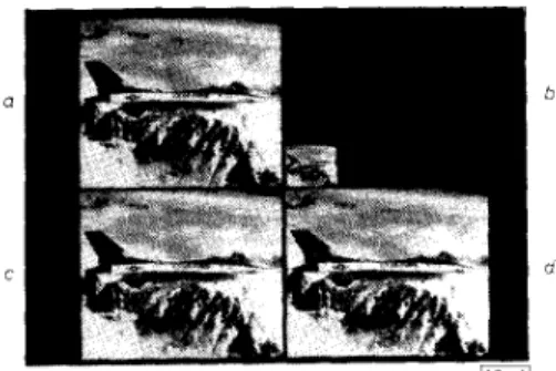
To investigate its performance, image data are interpolated by this circuit via computer simulation. For comparison, the same data are also interpolated by the conventional sinc inter- polation. A truncated Hamming-sinc lowpass filter is used in the sinc method. For both methods, the data are interpolated first row by row and then column by column. The results of the experiment are shown in Fig. 2. The original image is first decimated by two and then interpolated by both methods.
Fig. 2 Original image, decimated image. image interpolated by proposed
method, and image interpolated by sinc method a Original
b Decimated ( M = 2)
c Interpolated by proposed method
d Interpolated by sinc method ELECTRONICS LETTERS 23rd A w i l 1992 Vol. 28 No. 9
1
Another experiment with a decimation factor of four is shown in Fig. 3. It can be seen that the performance of the proposed method is compatible with that of the conventional method.
1
Fig. 3 Original image after preprocess of lowpass filter, deciniated image, image interpolated by proposed method, and image interpolated by sinc method
R Original h Decimated ( M = 4)
c Interpolated by proposed method
d Interpolated by s ~ n c method
Conclusion: An analogue circuit has been derived for image interpolation. Experimental results show that this circuit yields acceptable performance. With its regular structure. it is suitable for integrated circuit implementation to achieve high speed interpolation.
lflth March 1992 H.-C. Hsieh and W.-T. Chang* (Image and Signal Prmvzsrriy Lohor- ator.y, Department of Communication Engineering, Nutional Chiao Tung University, Hsinchu, Taiwan. Republic oj Chino)
*
Corresponding author References1 PARKER, J . A., KENYON, R. v.. and TROXEL, I) :E 'Comparison of interpolating methods for image resampling'. I E E E Trans. Medical Imaging, 1983, 2, pp. 31-39
2 MEAD, c.: 'Analog VLSl and neural systems' (Addison-Wesley, Readings, MA, 1989)
3 HSlEH, H. c., and CHANG, w. I.: 'Analog computation Structure for surface reconstruction'. J . Visual Communication und Image Repre- sentation, 1991, 2, pp. 381-394
GRADUALLY-ON STRUCTURE
FOR
SCANDESIGN
P.
C. C h e n ,J.
F. Wangand
B. D. Liu
Indexing terms' Built-in selfest. Integrated circuits A new structure named the gradually-on (GO) Structure for the full/partial scan design of sequential circuits is proposed. Because this structure allows the scan cells to be turned on gradually, the total test application time can he dramatically reduced.
Introduction: Design for testability ( D F T ) is a method for simplifying the testing problem of sequential circuits. Among D F T techniques, scan design approaches now attract the most attention. The proposed scan design approaches can be classi- fied into full scan design [l] and partial scan design [2-5].* N o matter which approach is adopted, a considerable propor- tion of the actual testing time is spent in scanning bout the
*
CHEN, P. c., WAYU, I I.. ~ L H , c. P., and LIL, n. I). 'A new partial scan design based on hard fault distribution analysis'. Submitted for publication868
content of the scan chain, an operation which requires a number of clock pulses equal to the length of the scan chain.
In this letter, the gradually-on (GO) structure is introduced to reduce the test application time by adding a small amount of extra hardware. To indicate the superiority of the GO
structure over conventional structures, it is convenient to clas- sify the faults in a circuit under test (CUT) into four types. By investigating the influence of scan design on each type of fault, it is easy to conclude that the total test application time of the GO structure is less than that of conventional structures. GO sfruclure: For traditional scan structures, all the scan cells would be turned on (or o f f ) simultaneously. Usually. it is not necessary for a certain fault to be detected by scanning so many flipflops. For these approaches, the test application time for the test sequence of length
I
TI by scanning n flipflops isT A T = ( n
+
I ) xIT1
+ n (1)If the number of n could be adjusted to fit the requirement of detection of the target fault, the test application time could be reduced dramatically. The basic idea of the GO structure is to allow the scan cells of the scan cham to be turned o n grad- ually.
The topology of the GO structure is shown in Fig. 1. Without increasing the number of 110 pins, an extra shift register, named the mode control register (MCR), as shown in the shaded block, is added to control the mode of each tradi- tional scan cell such that the scan chain can be turned on gradually. The extra multiplexer-like function block is added to choose the scan-out path from the last turn-on scan cell and the select lines of this block are composed of the outputs of the MCR normal in normalout
I
4
I
alway high mode ;lock function block seltFig. I 'Topology 1 f G 0 .sirucIure
SI: Scan input, N I . normal input, NC: normal cloch. SC. scan clock, M : mode (on off), SO: scan output, N O : normal output, FF: Aiptlop
7'?a srhemc for GO .muc[ure. Because the GO structure allows the scan cells to be turned on gradually, the test sequence will be divided into n groups if there are n scan cells in the scan chain. Let
7;
represent the test sequence while i scan cells are turned on. Initially, all scan cells are off. To is applied to the C U T and the mode and scan clocks are held. AfterTo
is finished, the mode clock should be active to turn on the first scan cell in the scan chain, then the scan data can be scanned into the scan cell by triggering the scan clock. In the meantime, the contents of the scan cell are also scanned out. Now, the first vector in Ti can be applied to the CUT. The procedure for testing this type of circuit is described as follows:( I ) initially, the MCR i s 0 (2) apply
T,
to the C U T(3) send a mode clock to turn on the ith scan cell (initially,
i = 1)
(4) scan o u t the contents of the turn-on cell(s) while scanning data into the turn-on $can cell(s)
ELECTRONICS LETTERS 23rd Aprd 1992 Vol. 28 No 9