Analysis of instability line width and white wall created
by the photolithography process
Yang-Kuao Kuo*, Chuen-Guang Chao, Chi-Yuan Lin
Department of Materials Science and Engineering, National Chiao Tung University, 1001 Ta Hsueh Road, Hsinchu 30049, Taiwan, ROC Received 2 April 2004; received in revised form 24 June 2004; accepted 30 June 2004
Available online 12 September 2004
Abstract
In the photolithography processing of semiconductor, line width is smaller and smaller. Therefore, the requirements of process window are stricter than before. In the small line width, the formation of serious white wall will affect line width and cause rejects in following process. The study conducted research on the control of best focus in which particularly explored the relationship between exposure dose and line width and the phenomenon of white wall generated by focus. The research obtained related coefficients of exposure dose-line width and exposure dose-white wall by coating photo resist of different components with the same thickness on the surface of fused silica wafer. The results of research found that exposure dose might not only change line width but also had important effects on white wall. Among others, the most important factor for exposure dose is the component of sensitivity of photo resist.
q2004 Elsevier Ltd. All rights reserved. Keywords: Line width; White wall
1. Introduction
Wafer throughput in micro-lithography depends on the sensitivity of the resist film to radiation. A lower exposure time required to produce a latent image in the resist corresponds to a higher throughput [1]. The focus affects line width: a focus of 0 mm yields the lowest line width, the width increases with the focus distance. Positive and negative foci yield symmetrical results[2]. The line width and the resist thickness curve. The primary factor that dominates the gradient of the exposure/line width relation-ship is the resist’s internal chemical composition[3].
Resist spin coating has been successfully modeled using a detailed non-Newtonian analysis, which allows local fluid viscosity to vary with concentration and shear rate[4]. The cleavage of a butylester is acid-catalyzed and yields carboxcylic acid and isobutene after exposure to the photo active component (PAC) and post-exposure back (PEB)[5]. When an acid generator is present in a CAMP resist
formulation, the mechanism for producing a lithographic pattern is simple. The strong acid formed causes deprotec-tion at a relatively low temperature with an activadeprotec-tion energy of around 11–14 kcal/mol[6].
Resist is a photo-sensitive material. If exposed to common white light, a chemical reaction occurs and photolithography cannot be performed. The photolithogra-phy process is like the development of a photographic film in that it must be performed in a darkroom. The photolithographic process is further limited since a yellow light source does not promote the resist to react chemically. Accordingly, photolithography should be performed in an environment with a yellow light source [7–14]. The commonly used light sources in the stepper include the G-line, the I-line and deep ultraviolet (DUV). The G-line wavelength is w436 nm, the I-line lZ350–450 nm, and DUV lZ100–300 nm[15–17]. The wavelength of the I-line changes according to the internal composition and gas pressure of the mercury arc lamp used, varying within 350–450 nm. DUV wavelengths differ according to the laser gas composition: KrF lZ248 nm, ArF lZ193 nm and F2
lZ157 nm. In this work, the DUV stepper’s laser light source, KrF lZ248 nm, was used.
0026-2692/$ - see front matter q 2004 Elsevier Ltd. All rights reserved. doi:10.1016/j.mejo.2004.06.023
www.elsevier.com/locate/mejo
* Corresponding author. Tel.: C886-3-5731809; fax: C886-3-5724727. E-mail address: [email protected] (Y.-K. Kuo).
Photolithographic experiments depend on several kinds of measurement instruments. Moreover, the optical process involved is complex. The main aim is to reduce the line width and make the critical dimension (CD) bar even more stable, which is usually achieved by changing the light source
[18]. One method of improvement involves the reticle’s zoom ratio. However, a difference between the reticle’s zoom ratio and that is too large will cause the photolitho-graphic process not to be ideal[19,20]. In these experiments, the compression ratio applied to the pattern on the reticle and the wafer was 5:1. The compression ratio applied to the DUV was the same as for the I-line.
2. Experimental 2.1. Equipment
[1] The steppers were a Nikon I-line and DUV. The major function of a stepper is to apply the exposure pattern to the surface of a wafer that has already been coated with a layer of resist. The main difference between an I-line stepper and a DUV stepper is that they use different light sources. The light source used by an I-line stepper is a UV lamp lZ365 nm, while the light source used by a DUV stepper is a KrF excimer laser lZ248 nm. The differences between the wavelengths of these light sources lead to different resolutions. Generally, a shorter wavelength gives a better resolution, and a better resolution enables the line width to be made narrower.
The exposure field used by the I-line stepper was a 6 in./22 mm2 of glass material. The lens numerical aperture (LNA)Z0.60 and the input numerical aperture (INA)Z0.38. The numerical apertures (NAs) were fixed.
The exposure field used by the DUV stepper was a 6 in./22 mm2of glass material. LNAZ0.60 and INAZ0.45. The Nikon stepper has two NAs. The INA is the front-end of the lens through which the arc lamp or the laser light passes. The INA did no affect the experiment. The LNA is the NA close to the edge of the wafer and is directly affects the experiments. Hence, LNAZNA (sZINA/LNA, Illumination aperture used annular type). Generally, the NA of the DUV can be opened wider because the resolution of the resist used with DUV is higher than with the I-line.
[2] For scanning electron microscopy (SEM), the microscopes used were a Hitachi S-9200, a KLA_Tencor 8100, and a Applied Materials’ SEM Vision. The Hitachi S-9200’s primary function was to measure the pattern’s line width and the capture a top view of the image. The error correction method involved a standard wafer that, after etching, had a line width of 0.3 mmG10%. The line width of this standard wafer was measured and if the result was within 0.3 mmG10%, then the was considered to meet our requirements. The error between the results obtained by the KLA_Tencor and those obtained by the Hitachi S-9200 was not allowed to exceed G10%.
The applied materials SEM vision. This investigation used APPLIED materials SEM Vision to observe the free-space diagram of pattern and the composition of EDX measurement materials rather than using measurement of line width. The main advantage of this approach is that E-beam can measure the wafer surface under G458, thus indicating the free-space diagram and pattern variation.
[3] The TEL CLEAN ACT-8 machine was used for spin coating and as a developer. The main functions of the ACT-8 are (1) priming, (2) spin coating, (3) soft baking and (4) developing.
(1) A layer of Hexamethyldislazane (HMDS) is sprayed onto the wafer. HMDS functioned as a medium that strengthened the bond between resist and wafer surface. After suitable priming, the wafer surface energy can be adjusted to a level similar to the resist surface energy to increase the adhesive strength between the wafer surface and the resist. (2) After dehydration baking and priming, the liquid resist must be evenly applied to the wafer surface. The resist was dripped onto the center of the wafer and distributed over its surface by the centrifugal force due to high-speed rotation. A higher rotation speed yields a thinner and more uniform resist liquid. The resist includes a very volatile organic solvent. After the resist is sprinkled onto the wafer surface, the stickiness of the resist changes with the volatility of the solvent. Failing to complete the coating before the solvent becomes volatile yields poor uniformity. (3) The main purpose of the soft baking was to eliminate the solvent that remains in the resist after spin coating, to transform the resist from a semi-solid to a solid film. (4) The main purpose of developing was to display the pattern that followed the exposure and leave the required pattern after the developer reacts.
[4] After the coating process is completed, the thickness of the resist must be known. Therefore, a KLA_Tencor PROMETRIX UV-1280SE was used to measure the thickness of the resist film, by applying optical methods to measure accurately the thickness of the resist from the center of the wafer to the edges of the wafer after the resist has solidified.
2.2. Experimental
This experiment is designed to use matrix exposure to lay out horizontal and vertical axes and to utilize the combination of exposure to obtain variant conditions between line width and white wall. PR is subject to different optimal focus point resulting from different properties in terms of thickness and sensitivity. In this experiment, in order to attain the optimal focal point, each PR was calibrated to a focus of less than G0.1 mm before experiment. Then, matrix exposure method was used to set up the focus at the best focal position. By changing exposure dose, the results of experiment are obtained.
3. Results and discussion
3.1. Focus and exposure theory
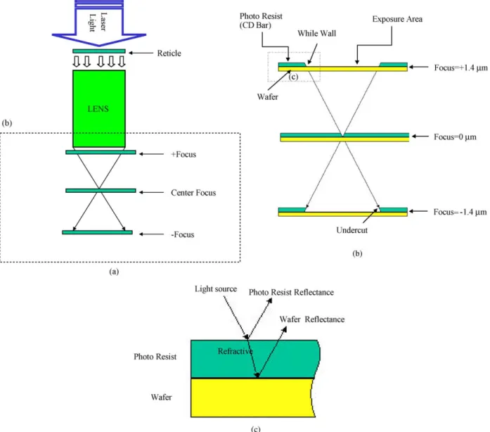
Fig. 1(b)clearly illustrates a cone shaped distribution and positive and negative symmetry of light sources from the lens to the wafer surface. Given focusZC1.4 mm and focusZK1.4 mm, the exposure area of CD bar exceeds focusZ0 mm. Consequently, the size of CD bar is not different given for focusZ0 mm and focusZG1.4 mm. Pattern length is longest when focusZ0 mm, because exposure area is smallest and pattern length is shortest when focusZG1.4 mm because exposure area is maxi-mized. However, these phenomenon only occur on positive resist. For negative resist opposite results are obtained. Positive resist is characterized by the lighted area producing photo-acid and alkali developer, which is eliminated following neutralization because of the balance between
acid and alkali. DUV light source has a cone shape distribution, and positive and negative symmetry exists between the lens and the wafer surface. When exposure location is on the top of the cone, then this investigation assumes focusZ0 mm. The focus distance increases with the distance of the exposure location from the top of the cone. The cone area is smallest when focusZ0 mm, and thus the lighted area is less than for focusZG1.4 mm while the pattern length is longer or bigger. The lighted area of positive resist increases given focusZG1.4 mm. Besides, probably because of the serious defocus or the reduced capacity to display diagram borders, pattern length is reduced and an irregular pattern forms given focusZG1.4 mm.
3.2. The impact of focus on white wall
Carboxylic acid can be produced after PR is exposed. This acid after its contact with base solution will be
Fig. 1. (a) Stepper exposure diagram, (b) Influence of focus on exposure area and (c) Focus locations following reflectance and refraction on photo resist and wafer surface by light source.
neutralized and dissolved. Basically, development process results in a neutralized reaction as PR is sprayed by developer, and it is considered as a severe impact in terms of affecting line width and white wall (Fig. 3). In this experiment, the development process used is the same for all wafers. Data obtained through this arrangement can be very accurate. After exposure, TMAH is used to neutralize wafer by having PR going through acid–base balanced reactions. The PR surface of wafer will produce different shapes because of the light going through a reticle in generating a cone-shrinking ratio of 4:1. When it is in positive focus, light will project onto the wafer surface with a reverse cone-shrinking ratio of 4:1 causing CD bar to have a shape of positive trapezoid (Fig. 4(b)), resulting from the usage of positive PR. If Cfocus is in the range of greater than the permitted thickness of PR, then CD bar has a shape of equilateral triangle. When it is in negative focus, light will project onto the wafer surface with right circular
cone-shrinking ratio of 4:1, thus causing CD bar to have a shape of reverse trapezoid. When the negative focus is greater than the range of permitted thickness of PR, then CD bar would collapse due to the lack of support from bottom. In this experiment, focus is restricted within the range of G0.1 mm. Therefore, the impact of focus on white wall is reduced to its minimum. Although this factor is reduced, the occurrence of white wall will still take place. The reason is that when TMAH is sprayed on the surface of PR, the neutralized reaction takes place on the surface first, then it extends into the bottom. As a result, the surface of PR has experienced longer time than that of bottom. Conse-quently, the white wall of CD bar forms a taper side (Fig. 4).
3.3. The impact of exposure dose on CD bar
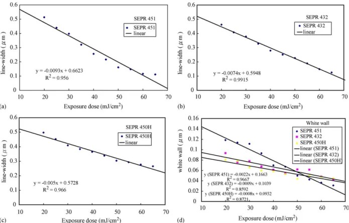
Exposure dose is a main factor in influencing line width. In this research, it is found that the higher the exposure dose the smaller is the line width. At the same time, exposure dose can affect white wall, i.e. the higher the exposure dose the smaller is the white wall. Furthermore, both exposure dose-line width and exposure dose-white wall contribute to the characteristics of linear relationship.
FromFig. 2, it can be seen by comparison that these three PR produce three different line widths and white walls when exposing them at the same energy. However, these three PR curves appear the same trend. That is, the higher the exposure dose, the smaller are the line width and the white wall. Under the same PR thickness, the main factor that affects the slope of exposure dose-line width and white wall is the sensitivity of PR. In other words, under the same energy, the higher the sensitivity, the smaller the line width becomes. In this experiment, under the condition of having the fixed film thickness of PR, the varied relationship of energy with respect to line width and white wall is studied. All three PR thickness are controlled at 7500G200 A˚ and the homogeneity of PR is at 3s!0.03 mm.
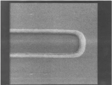
Fig. 2. DUV light source, SEPR-451 photo resist, exposure timeZ40 mJ/cm2, focusZ0 mm, observed with the Hitachi SEM at a magnification voltage of 50 kV. (i) line width, (ii) white wall.
Fig. 3. DUV light source, SEPR-432 photo resist, exposure doseZ30 mJ/cm2, observed with the Applied Materials SEM at a scanning angle of C458:
From Fig. 2, it is found that line width measured after exposed with high dose is much smaller than that when exposed with low dose, which is consistent with the results obtained from measuring white wall and line width. In addition, line width and exposure dose present the linear relationship, and white wall and exposure dose contribute to the linear relationship as well. When exposure dose is low, line width is wider than that exposed at high dose. This can be attributed to the facts that at high exposure dose, the absorption of high energy of PR enhances the reaction capability of neutralization. Therefore, there will be more areas to be neutralized. Those impurities after neutralization can be rapidly washed away by DI water. However, too high of exposure dose can cause line width to become very small. As a result, the aspect ratio becomes too large. Therefore, CD bar cannot hold back the turbulent force caused by DI water as neutralized area is washed, causing CD bar to collapse. FromFig. 5, it is revealed that SEPR-451 PR can cause CD bar to collapse at doseZ80 mJ/cm2. This resulted from the facts that the sensitivity of SEPR-451 is higher than that of the other two PR and can cause aspect ratio to become higher than that of the other two PR even at the same exposure dose. After development, SEPR-451 cannot support the impact of turbulent force and collapse. High energy can make light penetrate through the bottom of PR with high reflective energy coming out from bottom. Therefore, the area to be neutralized at the bottom of CD bar is increased. Hence, white wall decreases as
the exposure is increased, and it maintains a linear relationship with respect to exposure dose. FromFig. 2, it can be seen that the linear slope of exposure dose-white wall and dose-line width is different using the same PR. By comparing the slope of exposure dose-line width with that of exposure-white wall for three different PR, the slope of exposure dose-line width is higher, so is the slope of exposure-white wall. The main reason contributing to this trend is due to the sensitivity of PR. By comparing the
Table 1withFig. 2, it can be seen that the slope of exposure
Fig. 4. (a) SEPR-451, (b) SEPR-432, (c) SEPR-450H, correlation diagram of exposure dose and line width and (d) Graphs showing exposure dose vs. white wall for three different PR.
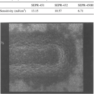
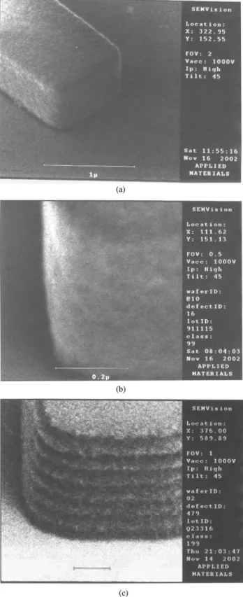
Fig. 5. Collapse of CD bar for SEPR-451 PR at exposure dose of 80 mJ/cm2, picture taken by Applied Materials SEM Vision.
dose-line width is much steeper for PR having higher sensitivity as compared to that having lower sensitivity. This arises from the fact that PR with higher sensitivity after its exposing to light source becomes relatively easy to produce neutralized reactions. Also, it can be found from
Fig. 2 that the sensitivity between SEPR-451 and SEPR-450H is off by 1.96 times. When exposure dose is at 20 mJ/cm2, line width can be off by 1.03 times. However, as exposure dose reaches to 65 mJ/cm2, line width can be different by 0.42 times. The outcome attained from this observation indicates that the higher the exposure dose, the more important the factor of sensitivity that can
affect on line width. As exposure dose is at 20 mJ/cm2, white wall is off by 1.46 times. While exposure dose reaches at 65 mJ/cm2, line width is off by 0.68 times. The ratio of white walls with their exposure doses at 20 or at 65 mJ/cm2 is 2.12. The ratio of line widths with their exposure doses at 20 or at 65 mJ/cm2is 2.45. From these two ratios, it can be found that the error caused by the impact of sensitivity with respect to line width and white wall is minimal.
FromFig. 6, exposure dose becomes too low, PR would not form a pattern due to the fact that the absorption of exposure energy by PR is not strong enough to produce a neutralized reaction when in contact with TMAH. On the contrary, From Fig. 7(a), high exposure energy makes CD bar become smaller. FromFig. 7(b), it can be found that too high of exposure dose can make CD bar become unstable. High exposure energy makes CD bar unstable and this step could cause an error if the wrong measurement point were selected. Therefore, the CD SEM measurement method we use is to measure a point for each 0.2 mm in length by selecting a center point on CD bar within a range of 2 mm for ten points. Then, take the average of these ten points to be the value of the line width.
3.4. Standing wave
The formation of standing wave is caused by areas having exposed the strongest light with the formation of the most abundant indene carboxylic acid (ICA). These exposed areas have the fastest dissolvable rate in alkaline solution and their dissolvable areas are the widest ones after development. On the other hand, the areas having exposed the weakest light show the narrowest dissolvable regions. As a result, PR after development forms a periodic contour pattern, i.e. wide and narrow side wall or (white wall). These wave patterns cannot be observed by using Hitachi S-9200 or KLA Tencor 8100 CD SEM. In order to observe these phenomena clearly, it is necessary
Table 1
Sensitivity of photo resist used in experiment
SEPR-451 SEPR-432 SEPR-450H
Sensitivity (mJ/cm2) 13.15 10.57 6.71
Fig. 6. Exposure dose becomes too low (10 mJ/cm2) for SEPR-450H PR, observed with the Hitachi SEM at a magnification voltage of 100 kV. PR would not form a pattern.
Fig. 7. (a) High exposure dose (50 mJ/cm2) makes CD bar become smaller, (b) Instability of CD bar caused by high exposure dose (60 mJ/cm2) for SEPR-432 PR, by Applied Materials SEM Vision.
to use Applied Materials SEM Vision to look at them by tilting wafer with 458 and/or use E-beam to examine by twisting wafer with G458. From this experiment, it is found that exposure dose does not affect the size of
standing wave. It can be attributed to the facts that the increment of exposure dose cannot change the wavelength of laser. But, coating top anti-reflection coating (ARC) and bottom ARC on the surface or bottom of PR can make the effect of standing wave reduced. From Fig. 8(a)–(c), by comparing PR in terms of adding top ARC and bottom ARC to SEPR-432, the standing wave becomes smaller after adding top ARC and bottom ARC to the PR as compared with using SEPR-432 PR along. In fact, we had problem using Applied Materials SEM Vision to locate for a periodic contour pattern of white wall with wide and narrow side wall caused by standing wave. This arises from the facts that the addition of top ARC or bottom ARC can improve the effectiveness of the refractive index and the absorbance of SEPR-432. In addition, different PR would produce different effects of standing wave because different PR possesses different refractive and absorbance. From Fig. 8, the contour patterns caused by standing wave resulting from three different types of PR are presented. When the refractive and the absorbance of PR per se are the same as those of top ARC or bottom ARC, the standing wave obtained from the PR produces the same effect as that of increasing top ARC or bottom ARC.
4. Conclusions
Due to the differences of the composition of sensitizer contained in each PR, as a result, the sensitivity of each PR shows great differences according to its characteristics. Sensitivity is an important factor in terms of absorbing light when PR is exposed. However, photoresists with good sensitivity do not produce the same good results consist-ently in terms of resolution. Therefore, sensitivity becomes one of the important components of PR. For PRs having the same sensitivity, their CD bars can be changed using different exposure doses. High exposure dose not only makes CD bar smaller, but also causes white wall to be relatively small. In other words, the side wall of CD bar becomes more vertical. Nevertheless, too high of exposure dose can make CD bar either unstable or even collapsible. It is worth mentioning that both exposure dose-line width and exposure dose-white wall appear to have the linear relationship. Statistically, when R2O0.7, data is regarded as highly correlated. In this experiment, our results indicate that R2O0.85, therefore, to be considered as a linear correlation.
Acknowledgements
The authors would like to thank the National Science Council of the Republic of China for financially supporting this research under Contract No. NSC 92216E009019.
Fig. 8. (a) Add top ARC to SEPR-432, (b) add bottom ARC to SEPR-432 and (c) SEPR-432 without adding any ARC, graphs showing standing wave as side wall of CD bar was observed via Applied Materials SEM Vision.
References
[1] T. Long, S.K. Obendorf, F. Rodriguez, Polym. Engng. Sci. 1589 (1992). [2] M.E. Preil, W.H. Arnold, Polym. Engng. Sci. 1583 (1992). [3] B. Kuyel, H. Sewell, J. Vac. Sci. Technol. 1385 (1990).
[4] W.W. Flack, D.S. Soong, A.T. Bell, D.W. Hess, J. Appl. Phys. 56 (4) (1984).
[5] R. Leuschner, H. Borndorfer, E. Kuhn, M. Sebald, R. Sezi, M. Byer, C.H. Nolscher, Polym. Engng. Sci. 1558 (1998).
[6] T.X. Neeman, F.M. Houlihan, E. Reichmanis, J. Kometani, B.J. Bachman, L.F. Thompson, Proc. SPIE 1086 (2) (1989). [7] R. Leuschner, H. Borndorfer, E. Kuhn, M. Sebald, R. Sezi, M. Byer,
C.H. Nolscher, Polym. Engng. Sci. 1558 (1998).
[8] Y. Matsuoka, K. Yokota, S. Ogitani, A. Ikeda, H. Takahashi, H. Ai, Polym. Engng. Sci. 1618 (1992).
[9] C.M. Garza, E.J. Solowiej, M.A. Boehm, Polym. Engng. Sci. 1600 (1992).
[10] A.E. Nader, K. Imai, J.D. Craig, C.N. Lazaridis, D.O. Murray III, M.T. Pottiger, S.A. Dombchik, W.J. Lautenberger, Polym. Engng. Sci. 1613 (1992).
[11] H. Nishizawa, K. Sato, M. Kojima, H. Satou, Polym. Engng. Sci. 1610 (1992).
[12] R.R. Kunz, M.W. Horn, Polym. Engng. Sci. 1595 (1992).
[13] C.M. Garza, E.L. Solowied, M.A. Boehm, Polym. Engng. Sci. 1600 (1992).
[14] A.E. Nader, K. Imai, J.D. Craig, C.N. Lazaridis, D.O. Murray, M.T. Pottiger, S.A. Dombchik, W.J. Lautenberger, Polym. Engng. Sci. 1613 (1992).
[15] C.A. Mack, Appl. Opt. 1958 (1986). [16] J.E. Korka, Appl. Opt. 969 (1970). [17] D.W. Widmann, Appl. Opt. 931 (1975).
[18] B.F. Griffing, P.R. West, Solid State Technol. 28 (152) (1985). [19] F.F. Shi, S. Yu, Thin Solid Films June 8 (1998) 254–258. [20] B. Fay, Microelectr. Engng. 61–62 (July) (2002) 11–24.