Design of Bidirectional and Low Power Consumption
Gate Driver in Amorphous Silicon Technology for
TFT-LCD Application
Guang-Ting Zheng, Po-Tsun Liu, Senior Member, IEEE, Meng-Chyi Wu, Senior Member, IEEE,
Li-Wei Chu, Member, IEEE, and Meng-Chuan Yang
Abstract—A new gate driver has been designed and fabricated by amorphous silicon (a-Si) technology. With utilizing four clock signals in the design of gate driver on array (GOA), the pull-up transistor has ability for both output charging and discharging, and layout size of the proposed gate driver can be narrowed for bezel panel application. Moreover, lower duty cycle of clock sig-nals can decrease static power loss to further reduce the overall power consumption of the proposed gate driver. The scan direction of the proposed gate driver can be adjusted by switching two direct control signals to present the reversal display of image. The pro-posed gate driver has been successfully demonstrated in a 4.5-inch WVGA 480 800 TFT-LCD panel and passed relia-bility tests of the supporting foundry.
Index Terms—Amorphous silicon (a-Si), gate driver, thin-film transistor liquid crystal display (TFT-LCD).
I. INTRODUCTION
I
N RECENT YEARS, a variety of portable electronic devices have been introduced with small displays such as cellular phone and PDA (Personal Digital Assistants). Dis-plays for portable electronic devices require high resolution, light-weight, and low power consumption. Therefore, the inte-grated gate driver using amorphous silicon (a-Si) technology for the TFT-LCD has become the main stream due to the mature manufacturing, low-cost processing, and elimination of the gate driver ICs [1]–[12]. Nevertheless, design of the integrated gate driver by a-Si encounters three main challenges which are the low field-effect mobility, low reliability issue under high voltage stress, and the lack of P-type transistor. In order to al-leviate the low mobility restriction, the thousands micro-meter width of the main driving TFT is required to drive the gate line of the panel. But the large parasitic capacitance affects the performance of circuit. In addition, the reliability issue of the Manuscript received May 31, 2012; revised August 05, 2012; accepted Oc-tober 09, 2012. Date of publication January 14, 2013; date of current version February 11, 2013. This work was supported by Giantplus Technology Corpo-ration, Taiwan, and supported in part by the National Science Council, Taiwan, under Contract NSC 100-2628-E-009-016-MY3.G.-T. Zheng and M.-C. Wu are with the Department of Electronics & Engineering Institute, National Tsing-Hua University, Hsinchu 30078, Taiwan (e-mail: [email protected]; [email protected]).
P.-T. Liu is with the Department of Photonics & Display Institute, National Chiao-Tung University, Hsinchu 30078, Taiwan (e-mail: [email protected]. tw).
L.-W. Chu and M.-C. Yang are with the Department of Photonics & Dis-play Institute, National Chiao-Tung University, Hsinchu 30078, Taiwan (e-mail: [email protected]; [email protected]).
Color versions of one or more of the figures are available online at http:// ieeexplore.ieee.org.
Digital Object Identifier 10.1109/JDT.2012.2225406
integrated gate driver is as well as a notable challenge. While a-Si TFT suffers the DC-bias shift which results from charge trapping and defect creation leads to shorten the life time of the integrated driver [13]–[17]. Besides, the structure of a-Si gate driver using only N-type transistor increase the difficulty of design for panel application.
So far, a-Si integrated gate driver was originated from Thomson’s shifter register which was made up of four transis-tors and one capacitor merely [2], [3], and many methods have been developed to improve the circuit [5]–[8]. For the prior arts, the circuit style of diode connection degrades the output rise time due to the threshold voltage drop on gate voltage of pull-up transistor, hence the before work [18] proposed a high rising time gate driver with a threshold voltage drop cancellation technique that decreases output rise time by 24.6% for high resolution display application. However, the switching times of clock signals (Clk and XClk) with 50% duty cycle and large size of pull-up and pull-down transistors in before work caused high power consumption.
Besides, Chun et al. [19] developed the bidirectional gate driver circuit with a-Si:H technology to change direction of vertical scan depending on the polarity of two control signals. Furthermore, Lin et al. [20] proposed a bidirectional gate driver circuit using the carrier buffer TFT to select the direction of transfer and does not suffer from the shift in the threshold voltage.
In this work, the pull-up transistor is designed to has ability for both output charging and discharging with low duty cycle (25%) clock signals in proposed gate driver circuit, and the par-asitic capacitances and layout size of gate driver are be nar-rowed for bezel panel application. Moreover, lower duty cycle of clock signals can decrease static power loss to further reduce the overall power consumption of the proposed gate driver. Be-sides, high performance bidirectional gate driver circuit is de-signed by simply switching two direct controlling signals with size reducing. The reversal display of image can easily be pre-sented in proposed gate driver by only exchanging the polarity of control signals.
II. OPERATION OF THEPROPOSEDINTEGRATEDGATEDRIVER A. Proposed Integrated Gate Driver for Single Direction Scanning
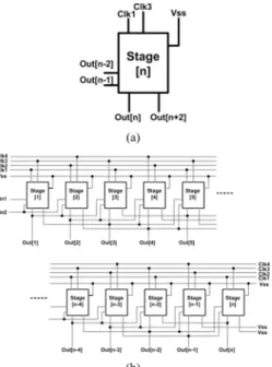
The block diagram of the proposed low power integrated gate driver circuit is shown in Fig. 1(a), which is composed of the 1551-319X/$31.00 © 2013 IEEE
Fig. 1. (a) Block diagram and (b) connections between stages of the proposed circuit for TFT-LCD application.
input signals ( and ), control signals (Clk1 and Clk3), feedback signal , and output signal . Fig. 1(b) depicts the connections among the proposed low power integrated gate driver circuit stages for TFT-LCD application. The block manipulation is activated while start sig-nals (In1 and In2) input a high voltage level to . A pulse signal is subsequently generated at and being acted as one of start signals for . Accordingly, sequential pulse signal can be periodically transferred stage by stage for feeding the whole gate lines of the pixel array in TFT-LCD.
Fig. 2(a) presents the schematic diagram of the proposed low power integrated gate driver with its corresponding waveforms in Fig. 2(b). The high and low voltage levels in Fig. 2(b) are de-fined as Vdd and Vss, respectively. Moreover, for the proposed circuit, the four clock signals have different phases and the duty of each clock signal is 25%. The operation can be divided into nine periods noted from T1 to T9. In the T1 period that Clk3 is high, M2, and M4 are turned on by Out[n-2] and Clk3. The other transistors are turned off. At this moment, is Vss through M4 and is charged by M2. Next, in the T2 pe-riod, only M1 is turned on and others are turned off. The is charger higher due to the second time charging. At the mean-while, the is still connects to Vss because of the on state of M3. After two periods of charging at , the final voltage is completely charge to Vdd-Vth.
In the T3 period, M1, M2, M4, and M5 are turned off by
, , Clk3, and . Clk1 becomes
high voltage level and then is charged by M3. At this moment, is boosted through Cb from Vdd-Vth to a higher voltage level which is labeled as Vb in Fig. 2(b). The high provides M3 charging with large current which is rela-tive to the width of M3 as well. On the other hand, M6 turns on slightly at the transient of Clk1 from Vss to Vdd. However, this turn on process is swift and turned off immediately because of M7 connects to high voltage previously.
Fig. 2. (a) Schematic and (b) corresponding operation waveforms of proposed circuit.
In the T4 period, all the TFTs and voltages maintain their last state except the discharges because Clk1 is low in this period as well as decreases to Vdd-Vth caused by coupling from the capacitor Cb. In other words, M3 is the main role for charging and discharging as shown in Fig. 3, the width of M4 is narrowed and the layout of the proposed gate driver can be constructed with miniature size. Then, in T5 period, M4 and M5 are turned on by Clk3 and . Others keep at off states and is discharged to Vss an is maintaining at Vss because of M4. Although the discharge capacity of M5 is not strong enough, the speed of discharge doesn’t influence the operation because Clk1 is at low voltage which is connected to while is at high voltage. The steps of delivering a gate line pulse at complete the remaining operation periods are used for the noise immunity.
In T6 period, the is stationary, and are
kept at low voltage. Next period, T7, which Clk1 is high and results in noise, the is coupled by Clk1 through parasitic capacitances and results in charging at . At meanwhile, M6 is used for eliminating the noise at . The Clk1 couples through C1, which is large enough to get high couple voltage at , and M6 is turned on by so as to discharge the disturbance at .
In the T8 period, the Clk1 transits from high to low voltage level at the beginning of this period. The variation is coupled to and affects , this makes voltages of and become slightly negative. Finally, in T9 period, M4 is turned on by Clk3 and then connects with Vss, that is, make sure is stable at low voltage level. Successively, the following periods replicate the steps from T6 to T9 orderly until the next start signals (In1 and In2) come up.
Fig. 3. Charge and discharge path by M3 for proposed circuit.
Fig. 4. (a) Block diagram and (b) connections between the stages of the proposed bidirectional gate drivers for TFT-LCD application.
B. Proposed Integrated Gate Driver for Bidirectional Scanning
The block diagram of the bidirectional gate driver is shown in Fig. 4(a), which is composed of one input signals , control signals (Clk1, Clk3, Vdd_f and Vdd_b), feedback sig-nals , and output signals . Fig. 4(b) depicts the connections of the driver blocks. For the forward scan di-rection, the block manipulation is activated while two start sig-nals (In1_f and In2_f) input a high voltage level to and . A pulse signal is subsequently generated at and being acted as the start signal for . Accordingly, sequen-tial pulse signal can be periodically transferred stage by stage for feeding the whole gate lines of the pixel array in TFT-LCD. On the other hand, for the backward scanning, the start sig-nals (In1_b and In2_b) are the impetus of the panel operation
Fig. 5. (a) Schematic and (b) corresponding operation waveforms of bidirec-tional gate driver circuit.
at that is the last stage of the gate driver circuit. The is the initiative signal of , and then the gate pulse appear at . Repeatedly, the operation among
blocks is the same as the forward direction. The only difference is the opposite of the order of gate pulses.
Fig. 5(a) presents the schematic diagram of bidirectional gate driver circuit with its corresponding waveforms in Fig. 5(b). The high and low voltage levels in Fig. 5(b) are defined as Vdd and Vss, respectively. The operation of bidirectional gate driver circuit is similar to the original proposed circuit.
For forward scanning, the Vdd_f and Vdd_b are connected to Vdd and Vss, respectively. And the operation steps can be divided into nine periods, noted from T1 to T9. The T1 to T9 periods are the same as mentioned in Fig. 2 except the lack of M1. For the backward direction, the sequences of clock signals have been adjusted and the voltage level of Vdd_f and Vdd_b has to be exchanged. The operation is similar to forward direc-tion where M2_b is used to charge the capacitor (Cb) in order to set node to high voltage level, and is reset by M1_f.
III. EXPERIMENTALRESULTS ANDDISCUSSION A. Simulation of the Proposed Integrated Gate Driver
The proposed integrated gate driver was designed and verified by HSPICE simulation with RPI a-Si TFT model provided by the foundry. The field-effect mo-bility and threshold voltage are 0.369 cm V s and 4.019 V, respectively. Table I indicates the device parameter (channel width (W) to channel length (L) aspect ratio and capacitors) of the proposed gate driver with the output loadings of each stage are one capacitor (17 pF) in parallel with one resistor (10 M ). The width of M3 of the proposed gate driver is designed with thousands micrometer for faster to pulling up and down the output loading of oscilloscope.
The input signals are two start pulses (In1 and In2), four clock signals (Clk1, Clk2, Clk3, and Clk4), and ground signal (Vss) with voltage levels from 25 to 0 V. Notice that the pulse width of each clock signal is 40 s with the operational period time of 160 s means the clock duty is 25%. Furthermore, a quarter
Fig. 6. Simulated waveforms of for the proposed circuit.
TABLE II
SIMULATEDRESULTS OF THEPROPOSEDCIRCUIT AT THEFIRST TO THEFOURTHOUTPUT
of clock duty reduces the stress effect of prominent transistors cause of low stress time for TFT, especially the pull down tran-sistor of M4.
1) Simulation of the Proposed Integrated Gate Driver for Single Direction Scanning: Fig. 6 illustrates the simulated waveforms of the proposed circuit from the first to the fourth stage. Sequential pulse signals have been successfully observed in Fig. 6 to verify the output function of proposed circuit. The rise time, fall time, and noise root mean square (RMS) voltage are represented in Table II, where the rise and fall times are defined by the time difference between 10% to 90% pulse voltage levels, the noise RMS is the root mean square voltage of from T6 to T9 periods.
The power consumption of GOA is calculated from the clock signals and it can be divided into two parts: dynamic and static power, which are shown as follows:
(1) The first term is the dynamic power loss from clock signals’ transition. Where A is the fraction of gate actively switching, C is the input loading capacitance of GOA cells, f is the frequency of clock, and n is the whole number of clocks in gate driver. In the proposed circuit, although the number of clocks is doubled, the frequency of clocks and the capacitance of the same clock signal are reduced by half. It means that the dynamic power is halved in the proposed gate driver. Moreover, the proposed circuit deserts the pull-down transistor in before works to reduce the overall parasitic capacitance of GOA cells, so the dynamic power consumption is substantially reduced cause of smaller input loading capacitance.
Fig. 7. Simulated output waveforms of bidirectional gate driver circuit at the
outputs , , , , , , and
. (a) Forward direction and (b) backward direction.
The second term presents the static power loss from the static current I and voltage source V and the main static power loss of GOA cells is from the leakage current of M3 (when
, , and in Fig. 2(a)), which is
operated in forward sub-threshold region and its formula can be depicted as [21]
(2) where and are the effective channel width and channel length. denotes the boundary of the forward sub-threshold. Sf is the forward sub-threshold slope, is the magnitude of current in the sub-threshold region, and is gate to source voltage. For the TFT-LCD panel application, when switching transistor in pixel is turned off, the gate to source voltage of it is about 7 V and the leakage current is low. Nevertheless, when of GOA is Vss, the gate to source voltage of M3 is about 0 V and it induces larger leakage current to result higher static power consumption of GOA cells. For this reason, the lower duty cycle of clock signals of the proposed gate driver (25%) will reduce the duration of high voltage of the pull-up transistor
TABLE III
COMPARISON OFPOWERSIMULATIONBETWEENPROPOSEDCIRCUIT AND
BEFOREWORKS
TABLE IV
SIMULATEDRESULTS OFBIDIRECTIONALGATEDRIVERCIRCUIT FORFORWARD
SCANNING ANDBACKWARDSCANNING
(M3) that can achieve lower static power consumption. Con-sequently, Table III shows the average power of the proposed circuit (12.57 mW) which is much lower than the before work (32.2 mW) [18], and the overall power reduction ratio is about 61%.
2) Simulation of the Proposed Integrated Gate Driver for Bidirectional Scanning: Fig. 7(a) and (b) show the simulated waveforms of the proposed bidirectional gate driver circuit for forward and backward scanning. The simulated outputs results are shown in Table IV. Notices that the first outputs ( and
) and final outputs ( and ) are dummy
stages and they are not shown in Fig. 7(a) and (b) Since the of dummy stages has no extra source such as M2_b in Fig. 5(a) to discharge it, the will be high if the Clk is in high period. Nevertheless, although the outputs of dummy stages are malfunction, there is no effect on the consequences of bidirectional gate driver circuit since they are not used to the gate lines of panel.
Fig. 8. (a) Measurement setups; (b) die photo of the proposed integrated gate driver; and (c) bidirectional gate driver for array testing. B. Measurement of the Proposed Integrated Gate Driver
For array verification, one hundred integrated gate driver which are manufactured on glass substrate in amorphous silicon technology. As shown in Fig. 8(a), the measurement setups depict that the synchronous control signals (Clk, XClk, and In) are generated by the pulse card option for Keithley 4200 (4200-PG2), and the input range are set as 0 V to 25 V. Furthermore, digital oscilloscope is utilized to observe the output waveforms. The equivalent loading of its probes is one capacitor (17 pF) in parallel with one resistor (10 M ) which is equal to the simulation environment. Moreover, the probe card with 24 pins is applied for the connections between fab-ricated circuit and measurement equipments. Fig. 8(b) and (c) present the die photo of the proposed integrated gate driver and bidirectional gate driver circuit. Because the widths of M3 is designed with thousands micrometer for pulling up and down the output node , the larger layout area is occupied by M3 in Fig. 8(b) and (c).
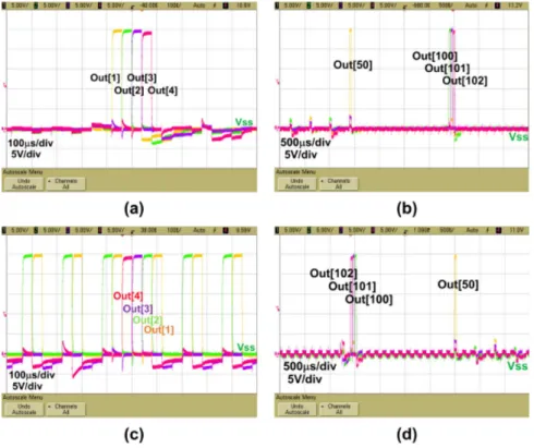
1) Measurement of the Proposed Integrated Gate Driver for Single Direction: Fig. 9(a) shows the measured output waveforms of the gate driver circuit for single direction from
the first to fourth stages ( , , , and )
and , , , and are shown
in Fig. 9(b) The rising time, falling time, and noise RMS are represented in Table V.
2) Measurement of the Proposed Integrated Gate Driver for Single Direction: Fig. 10(a) and (c) shows the measured output waveforms of the bidirectional gate driver circuit from
the first to fourth stages ( , , , and )
for the forward scanning and backward scanning. In addition,
, , , and are shown in
Fig. 9. Measured output waveforms of the proposed gate driver circuit at: (a)
head stages ( , , , and ) and (b) tail stages ( ,
, , ).
Fig. 10(b) and (d). The rising time, falling time, and noise RMS are represented in Table VI.
Notice that in Fig. 10 the outputs of final two stages for back-ward scanning, and , are malfunction because has no extra source such as M2_b in Fig. 5(a) to discharge
Fig. 10. Measured output waveforms of the bidirectional gate driver circuit by forward scanning for (a) ( , , , and ) (b) ,
, and ) and by backward scanning (c) ( , , , and ) (b) , , and ).
TABLE V
MEASUREDRESULTS OF THEPROPOSEDGATEDRIVERCIRCUIT AT THEHEAD
STAGES( , , ,AND ) (B) TAILSTAGES( ,
, , )
it, therefore, the will be high if the Clk is in high period. Although the outputs of dummy stages are malfunction, there is no effect on the consequences of bidirectional gate driver circuit since they are not used to the gate lines of panel.
C. Panel Integration of the Proposed Integrated Gate Driver A 4.5-inch WVGA panel has been fabricated with the pro-posed integrated gate driver, and its specification is summarized in Table VII. The resolution of the panel is
with the contrast ratio of 1000:1 and the frame rate is 60 Hz, respectively.
Besides, the demonstrated 4.5-inch panels are passed the reliability tests of the supporting foundry for operating after the 1000 hours operation under 70 and conditions. Fig. 11 presents the photo of the proposed integrated gate
TABLE VI
MEASUREDRESULTS OF THEPROPOSEDBIDIRECTIONALGATEDRIVER
CIRCUIT FORFORWARDSCANNING ANDBACKWARDSCANNING
drivers that are allocated at the both sides of pixel array in a 4.5-inch WVGA panel. The layout area of each stage is 950 m 207 m under the layout optimization and the RC load
Fig. 11. Photo of the proposed integrated gate drivers that are allocated at the both sides of pixel array in a 4.5-inch WVGA panel.
Fig. 12. Display image of a 4.5-inch WVGA panel for: (a) forward direction and (b) backward directions.
for each stage of gate driver is 2.62 for resistance and 40.4 pF for capacitance. For the sizes of TFTs of gate driver on panel are the some as the simulated sizes of TFTs. Fig. 12(a)
one output charge/discharge TFT to narrow the pixel size and achieve power reduction about 61%. Besides, the scan direction of the proposed gate driver can be adjusted by switching two control signals to accomplish the bidirectional function and it is as well as demonstrated on 4.5-inch WVGA panel successfully. Therefore, the proposed gate driver is quite appropriate for integration into to the high resolution and low power TFT-LCD panels.
REFERENCES
[1] R. Huq and S. Weisbrod, “Phase clocked shift register with cross con-necting between stages,” U.S. Patent 5 434 899, Jul. 18, 1995. [2] H. Lebrun, F. Maurice, J. Magarino, and N. Szydlo, “AMLCD with
integrated drivers made with amorphous-silicon TFTs,” SID Dig. Tech.
Papers, pp. 403–406, 1995.
[3] F. Maurice, H. Lebrun, N. Szydlo, U. Rossini, and R. Chaudet, “High resolution projection valve with the amorphous silicon AMLCD tech-nology,” in Proc. SPIE, 1998, pp. 92–99.
[4] T.-C. Huang, K.-T. Cheng, H.-Y. Tseng, and C.-P. Kung, “Reliability analysis for flexible electronics: Case study of integrated a-Si:H TFT scan driver,” J. Emerg. Technol. Comput. Syst., vol. 4, no. 3, pp. 1–23, Aug. 2008.
[5] J.-H. Oh, J.-H. Hur, Y.-D. Son, K.-M. Kim, S.-H. Kim, E.-H. Kim, J.-W. Choi, S.-M. Hong, J.-O. Kim, B.-S. Bae, and J. Jang, “2.0 inch a-Si:H TFT-LCD with low noise integrated gate driver,” SID Dig. Tech.
Papers, pp. 942–945, 2005.
[6] S.-Y. Yoon, Y.-H. Jang, B. Kim, M.-D. Chun, H.-N. Cho, N.-W. Cho, C.-Y. Sohn, S.-H. Jo, C.-D. Kim, and I.-J. Chung, “Highly stable in-tegrated gate driver circuit using a-Si TFT with dual pull-down struc-ture,” SID Dig. Tech. Papers, pp. 348–351, 2006.
[7] S. Edo, M. Wakagi, and S. Komura, ““A 2.2” QVGA a-Si TFT LCD with high reliability integrated gate driver,” SID Dig. Tech. Papers, pp. 1551–1552, 2006.
[8] J.-W. Choi, J.-I. Kim, S.-H. Kim, and J. Jang, “Highly reliable amor-phous silicon gate driver using stable center-offset thin-film transis-tors,” IEEE Trans. Electron Devices, vol. 57, no. 9, pp. 2330–2334, Sep. 2010.
[9] C.-L. Lin, C.-D. Tu, M.-C. Chuang, and J.-S. Yu, “Design of bidi-rectional and highly stable integrated hydrogenated amorphous silicon gate driver circuits,” J. Display Technol., vol. 7, no. 1, pp. 10–18, Jan. 2011.
[10] B. Kim and S.-Y. Yoon, “Shift Register,” United States Patent 7477226, Jan. 13, 2009.
[11] S.-H. Moon, “Shift register and driving method thereof,” U.S. Patent 7 532 701, May 12, 2009.
[12] C.-L. Lin, C.-D. Tu, M.-C. Chuang, K.-W. Chou, and C.-C. Hung, “A highly stable a-Si:H TFT gate driver circuit with reducing clock duty ratio,” Sid Dig. Tech. papers, pp. 1360–1362, 2010.
[13] M. Powell, “The physics of amorphous-silicon thin-film transistors,”
IEEE Trans. Electron Devices, vol. 36, no. 12, pp. 2753–2763, Dec.
1989.
[14] D. Allee, L. Clark, R. Shringarpure, S. Venugopal, Z.-P. Li, and E. Bawolek, “Degradation effects in a-Si:H thin film transistors and their impact on circuit performance,” in Proc. IRPS, 2008, pp. 158–167. [15] N. Ibaraki, M. Kigoshi, K. Fukuda, and J. Kigoshi, “Threshold voltage
instability of a-Si:H TFTs in liquid crystal displays,” J. Non-Cryst.
Solids, vol. 115, no. 1–3, pp. 138–140, 1989.
[16] H. Cheng, C. Huang, J. Lin, and J. Kung, “The reliability of amorphous silicon thin film transistors for LCD under DC and AC stresses,” in
[17] D. Allee, L. Clark, B. Vogt, R. Shringarpure, S. Venugopal, S. Uppili, K. Kaftanoglu, H. Shivalingaiah, Z.-P. Li, J. Fernando, E. Bawolek, and S. O’Rourke, “Circuit-level impact of a-Si:H thin-film-transistor degradation on effects,” IEEE Trans. Electron Devices, vol. 56, no. 6, pp. 1166–1176, Jun. 2009.
[18] L.-W. Chu, P.-T. Liu, and M.-D. Ker, “Design of integrated gate driver with threshold voltage drop cancellation in amorphous silicon tech-nology for TFT-LCD application,” J. Display Technol., vol. 7, no. 12, pp. 657–664, Dec. 2011.
[19] M. D. Chun, S. Y. Yoon, Y. H. Jang, K. S. Park, H. Y. Kim, B. Kim, H. N. Cho, S. C. Choi, T. W. Moon, N. W. Cho, S. H. Jo, C. Y. Sohn, C. D. Kim, and I. J. Chung, “Bi-directional integrated a-Si gate driver circuit for LCD panel with RGBW quad subpixels,” in Proc. ASID’06, 2006, pp. 125–127.
[20] C.-L. Lin, C.-D. Tu, M.-C. Chuang, and J.-S. Yu, “Design of bidi-rectional and highly stable integrated hydrogenated amorphous silicon gate driver circuits,” J. Display Technol., vol. 7, no. 1, pp. 10–18, Jan. 2011.
[21] Y. Kuo, Thin Film Transistors: Materials and Processes. New York: Kluwer, 2004, vol. 1.
Guang-Ting Zheng received the B.S. degree from the Biomedical Engineering and Environmental Sciences, National Tsing Hua University, Taiwan, in 2008, and the M.S. degree in electro-optical engineering from National Chiao Tung University, Taiwan, in 2010. Since August 2010, he has been working toward the Ph.D. degree at the National Tsing Hua University.
His current research interests include the periph-eral circuits integrated on panel for flat panel display applications
Po-Tsun Liu (A’06–SM’07) received the Ph.D. degree from the Institute of Electronics, National Chiao-Tung University (NCTU), Hsinchu, Taiwan, in 2000.
He is a professor and director at the Department of Photonics and Display Institute, NCTU, Taiwan. He also was a visiting professor at the Department of Electrical Engineering at Stanford University, CA, USA, from August 2008 to July 2009. In his specialty, he has made a great deal of pioneering contributions to ULSI technology, semiconductor memory devices and TFT-LCD Displays. In his previous researches on low-dielectric-constant (low-k) materials and copper interconnects, he utilized hydrogen plasma treatment technique for the first time to improve electrical characteristics of low-k silicate-based materials and to resist copper diffusion. In addition, he proposed a low-temperature supercritical carbon dioxide fluids SCCO technology for the first time to improve the dielectric characteristics of the sputter-deposited HfO film by passivating trap states. His current researches focus on the advanced flat panel display device technologies, spe-cialized in thin film transistors (TFTs), the advanced nano-scale semiconductor devices, nonvolatile memory devices, and nano-fabrication technologies. So far, he has published 150 articles of SCI international journals/letters, 80
international conference papers and obtained 17 U.S. patents and 46 Taiwan patents.
Dr. Liu is a member of Society for Information Display. Because of the promi-nent contributions, he was selected in Marquis Who’s Who in the World (20th edition, 2003) and obtained 2007 Outstanding Young Electrical Engineer Award of Chinese Institute of Electrical Engineering. Furthermore, he has superior per-formance in teaching, and obtained twice Excellent Teaching Awards at NCTU.
Meng-Chyi Wu (A’03–SM’03) was born on November 17, 1957, in Taipei, Taiwan. He received the B.S., M.S., and Ph.D. degrees in electrical engi-neering from the National Cheng Kung University, Taiwan in 1981, 1983, and 1986, respectively.
He is a professor in the Electrical Engineering Department of the National Tsing Hua University. He has over 22 years of research experience on III–V compound semiconductors, material char-acterization, optoelectronic devices, and epitaxial techniques consisting of liquid-phase epitaxy, MOCVD, and MBE. He was first to fabricate red AlGaAs/InGaP LEDs in Taiwan, which helps the development of visible LEDs grown by MOCVD. He also fabricated the long-wavelength InGaAsP/InP and AlGaInAs/InP laser diodes (LDs), which contain ridge-waveguide, distributed feedback, and vertical surface-emitting structures, for fiber communication applications. He also fabricated the first high speed (10 GHz) InGaAs/InP and InGaP/GaAs p-i-n photodiodes (PDs) with enhanced wide spectral range of 0.6–1.7 m and 300–900 nm, respectively. In addition, he also integrated p-i-n photodiode with the ruby micro-ball-lens for the alignment tolerance enhancement. He also developed vertical organic thin-film transistors (OTFTs) and transparent conductive oxides for the applications on the optoelectronic devices and displays. He has published over 245 journal papers.
Li-Wei Chu (S’10–M’12) received the B.S. degree from the Department of Electrical Engineering, National Sun Yat-sen University, Taiwan, in 2006, and the M.S. degree in electro-optical engineering from National Chiao Tung University, Taiwan, in 2008. Since August 2008, he has been working toward the Ph.D. degree at the National Chiao Tung University.
His current research interests include the periph-eral circuits integrated on panel for flat panel display applications and the design of 60 GHz ESD protec-tion circuits in 65 nm CMOS process.
Meng-Chuan Yang received the B.S. degree from the Department of Elec-trical Engineering, National Sun Yat-sen University, Taiwan, in 2008, and the M.S. degree in electro-optical engineering from National Chiao Tung Univer-sity, Taiwan, in 2010.
His current research interests include the peripheral circuits integrated on panel for flat panel display applications