國 立 交 通 大 學
電 子 工 程 學 系 電 子 研 究 所
碩 士 論 文
高效能之NAND型快閃記憶體控制器
HIGH-PERFORMANCE NAND FLASH
CONTROLLER
研 究 生:高于翔
指導教授:黃俊達 博士
高效能之NAND型快閃記憶體控制器
High-Performance NAND Flash Controller
研 究 生:高于翔 Student: Yu-Hsiang Kao
指導教授:黃 俊 達 博士 Advisor: Dr. Juinn-Dar Huang
國立交通大學
電子工程學系 電子研究所
碩士論文
A Thesis
Submitted to Department of Electronics Engineering & Institute of Electronics College of Electrical and Computer Engineering
National Chiao Tung University in Partial Fulfillment of the Requirements
for the Degree of Master in
高效能之NAND型快閃記憶體控制器
研究生:高于翔 指導教授:黃 俊 達 博士 國立交通大學 電子工程學系 電子研究所摘 要
NAND型快閃記憶體之小面積及低功耗使之成為現今最重要的非揮發性記憶元 件之一。它快速的讀寫時間讓其非常適合成為次世代之大量儲存媒介。然而,NAND 型快閃記憶體的輸出入介面之工作頻率限制了資料傳輸的頻寬。為了在此頻寬限 制下得到更高的效能,新世代的NAND型快閃記憶體元件提供交錯以及雙面運行之 指令。因此 NAND型快閃記憶體控制器也必須擁有支援這些先進指令集之能力以使 整體之系統效能提升。 在本篇論文中,我們提出一個高效能之NAND型快閃記憶體控制器。它主要使 用了兩項技巧,包括平行化指令處理及使用雙面指令之定址模式。藉由這些技巧, 我們可以盡可能地將指令間的平行度最大化並降低單一指令平均之執行時間以得 到較好的效能。實驗結果顯示,我們所提出的快閃記憶體控制器相較於一般基本 功能之控制器在各種讀寫之效能均可提升達18%以上。High-Performance NAND Flash Controller
Student: Yu-Hsiang Kao Advisor: Dr. Juinn-Dar Huang
Department of Electronics Engineering & Institute of Electronics National Chiao Tung University
Abstract
NAND flash memory is one of the most important components in non-volatile storage media because of its small size and low power consumption. Its fast erase and program time has made NAND flash very suitable for the new generation mass-storage device. However, the I/O interface frequency of NAND flash has limited the bandwidth of data transfer. In order to achieve higher performance under this bandwidth limitation, NAND flash device provides interleaved and two-plane command sets. Therefore, NAND flash controller must have the ability to enhance the related functionality to improve the overall system performance.
In this thesis, we propose a high-performance NAND flash controller by utilizing the two techniques, including out-of-order execution with multi-die commands and the two-plane addressing mode. By these techniques, we can maximize the commands being executed in parallel and shorten the average execution time per instruction to achieve
誌 謝
能夠順利完成本篇論文,首先我要感謝我的指導教授-黃俊達博士,在碩士兩 年期間給我的教導與支持。讓我得以在自由的風氣下學習,培養獨立思考的能力, 並適時的給予寶貴的意見及指導,感激之情非三言兩語得以表達。 接下來我要感謝我的父母以及男友,他們無條件且不求回報的支持以及對我無 微不至的關心,讓我一路走來能無後顧之憂。沒有他們,就沒有今天的我。 我也要感謝我的口試委員-張世杰教授、馬席彬教授和黃稚存教授。感謝他們 在百忙之中願意抽空前來給予我指導,讓我受益匪淺。 感謝所有ACAR Lab的成員,之暉、南興、哲霖、詠翔、建德、瀚蔚還有威虢學 長在研究的路上給予我的幫助,大家一起學習、努力的感覺真的很好。感謝所有 317B的成員,家宏、亞謙、彥廷、婉玲、柏丞、泓懌、尊宇、宗瀚、杰叡、時穎 還有所有學長姐學弟妹們。與你們在實驗室度過的時光是我人生中最美好的回 憶,希望大家的感情可以歷久彌新,不要斷了聯絡。 要感謝的人實在太多了,最後就謝天吧!Contents
中文摘要 ...i
English Abstract ... ii
誌謝 ... iii
Contents ...iv
Lists of Tables ...vi
Lists of Figures ... vii
Chapter 1 Introduction ... 1
1.1 Motivation ... 1
1.2 Overview of the proposed flash controller ... 2
1.3 Thesis organization ... 3
Chapter 2 Physical Properties of NAND Flash ... 4
2.1 Cell array organization ... 4
2.2 SLCVS.MLC ... 6
2.3 Operation principles ... 7
2.4 Basic NAND flash array ... 8
2.5 Advanced NAND flash array ... 10
Chapter 3 Functionalities of a Basic NAND Flash Controller ... 12
3.1 System architecture of NAND flash chip ... 12
3.2 The ONFi standard ... 13
3.3 Basic command management ... 14
Chapter 5 Experimental Results ... 28
5.1 Ideal Performance of commands ... 28
5.2 Experiment setup ... 30
5.3 EDA environment and synthesis result ... 31
5.4 NAND Flash simulation model ... 32
5.5 Experimental Results ... 32
Chapter 6 Conclusions and Future Works ... 36
List of Tables
Table 2.1: Comparisons between NAND and NOR flash ... 6
Table 5.1: Timing characteristic of different access... 28
Table 5.2: The ideal performance of NAND flash commands at a single die ... 29
Table 5.3: The EDA environment used for experiments ... 31
Table 5.4: The properties of the NAND flash model that used for simulation ... 32
Table 5.5: Experimental result of sequential read ... 33
Table 5.6: Experimental result of random read ... 33
Table 5.7: Experimental result of sequential program ... 34
List of Figures
Figure 2.1: Layout of a single flash memory cell ... 4
Figure 2.2: Array diagram of NAND and NOR memories ... 5
Figure 2.3: Voltage applied while reading – use 8-page block as an example... 7
Figure 2.4: Voltage applied while erasing ... 8
Figure 2.5: The NAND flash functional block diagram ... 8
Figure 2.6: Memory mapping of a NAND flash chip ... 10
Figure 2.7: Comparison between basic command and two-plane command ... 11
Figure 2.8: Difference between basic command and two-die command ... 11
Figure 3.1: The SSD system architecture ... 12
Figure 3.2: Timing diagram of ERASE operation ... 15
Figure 3.3: The READ timing diagram ... 16
Figure 4.1: The block diagram of advanced NAND flash device ... 18
Figure 4.2: Example of WAR prevention ... 22
Figure 4.3: The example of in-order commitment ... 23
Figure 4.4: Comparison between original and two-plane addressing mode ... 25
Figure 4.5: An example of interleaved command ... 26
Chapter 1
Introduction
1.1
Motivation
NAND flash memory was invented in 1980s by Dr. Fujio Masuoka. Due to its high cell density and relatively simple array architecture, NAND flash devices have found a strong foothold for solid-state mass storage [1]. In 2005, Toshiba and SanDisk developed a NAND flash chip capable of storing 1GB of data. Currently NAND flash based storage devices are widely used in applications such as removable storage, embedded storage and consumer electronic devices like memory cards, multimedia players or mobile phones [1], [2].
As integrated circuit techniques grow deeper with process miniaturization, the cell size of the flash memory has been scaled down 40%-50% per year [3], [4], and memory capacity also doubles every year [5]. The array organization of the NAND flash device is also enhanced from a single-plane, single-die array into a multi-plane, multi-die array whereas the instruction setup time and I/O transfer time remain almost the same while the
technology advances. In order to improve the performance of the NAND flash device, the NAND flash controller fully utilize those advanced features that the current NAND flash array provides.
When sequential data access occurs at chips using a conventional flash memory controller, only one page of data is accessed at a time, other commands in queue are waiting while the non-executing chips and dies remain idle, which indicates that the controller has poor parallelism [6]. For a conventional flash controller, the data throughput is completely determined by I/O frequency and command setup time. The performance of Micron MT29F32G08Q is 26MB/s for read and 4MB/s for program [7].
1.2
Overview of the proposed NAND flash controller
We propose a performance enhancing flash controller which has the advantage of simple hardware implementation by using the three methods as follows:
Parallel data access between chips and dies Two-plane addressing
Out-of-order execution
By these techniques, we can maximize the I/O data transfer rate and also decrease the command execution time of a single access to achieve a better performance.
The experimental results show that the proposed flash controller with 2 planes and 2 dies per chip can outperform the basic flash controller in all kinds of data accesses.
1.3
Thesis organization
This thesis introduces the high performance flash controller design, and is organized as follows. Chapter 2 explains the physical properties of NAND flash. Chapter 3 introduces the basic operations and the disadvantages of traditional flash controller. In Chapter 4 we present our high performance flash controller architecture. Chapter 5 shows the experimental results. Finally, Chapter 6 gives conclusions of this thesis.
Chapter 2
Physical Properties of NAND Flash
In this chapter, we will introduce the physical properties of NAND flash cell and its differences from traditional storage devices such as hard drives. Also we will introduce the overall array architecture of a complete NAND flash device.
2.1
Cell organization
Figure 2.1 shows the transistor configuration of a single flash cell [2]. By adding the floating gate into a traditional MOSFET, flash cell uses Flowler-Nordheim (FN) tunneling to drive stored electrons to memorize data after power off. Such Non-Volatile-Memory (NVM) characteristic and small cell area made flash be the popular choice as data storage.
Figure 2.1: Layout of a single flash memory cell
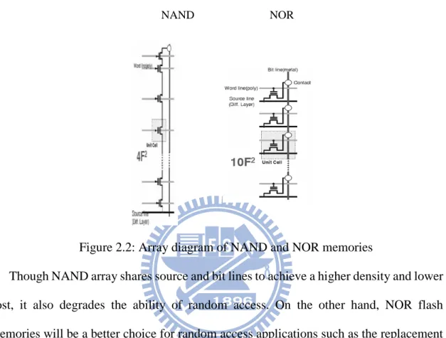
The cell array diagram of NAND and NOR memories are shown as Figure 2.2. Since NAND array shares both source lines and bit lines, its area per unit cell is only 40% of NOR array. Every word line of the NAND array represents a page entry, and the number
of word line which shares the same source line and bit line stands for the number of pages in a block. Block is the minimum unit of a NAND memory.
NAND NOR
Figure 2.2: Array diagram of NAND and NOR memories
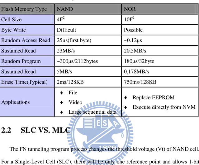
Though NAND array shares source and bit lines to achieve a higher density and lower cost, it also degrades the ability of random access. On the other hand, NOR flash memories will be a better choice for random access applications such as the replacement of EEPROM and uses as code memories. Other comparison of NAND and NOR memories are shown in Table 2.1. Since our target application is for large file storage, we choose NAND flash as the target for our controller architecture design.
Table 2.1: Comparisons between NAND and NOR flash
Flash Memory Type NAND NOR
Cell Size 4F2 10F2
Byte Write Difficult Possible
Random Access Read 25μs(first byte) ~0.12μs
Sustained Read 23MB/s 20.5MB/s
Random Program ~300μs/2112bytes 180μs/32byte
Sustained Read 5MB/s 0.178MB/s
Erase Time(Typical) 2ms/128KB 750ms/128KB
Applications
♦ File ♦ Video
♦ Large sequential data
♦ Replace EEPROM
♦ Execute directly from NVM
2.2
SLC VS. MLC
The FN tunneling program process changes the threshold voltage (Vt) of NAND cell. For a Single-Level Cell (SLC), there will be only one reference point and allows 1-bit operations per memory cell. On the other hand, the states stored in Multi-Level Cell (MLC) is determined by the number of Vt reference points, for instance, the most popular MLC cell has 3 reference points and stores 2-bit data per cell.
Since SLC has less reference point, it has higher performance and reliability. The endurance of SLC is ten times longer than MLC chips, and SLC chips also offer a shorter array operation time.
Generally, SLC chips require only 1 bit error correction code (ECC) per 512 bytes whereas MLC chips require 4 or more bits for ECC [2]. And SLC chips can operate at a lower voltage to achieve the same data integrity as MLC chips, which will be a better
choice to use in mobile applications. MLC chips gain advantages of its low manufacturing cost, capacity of a single chip doubles because of the number of bit stored in an MLC cell is twice as an SLC cell, thus it’s mainly used in consumer memory card, media player and applications where performance and reliability are not that important. Some applications also combined SLC and MLC chips together to obtain a better mix.
2.3
Operation principles
All array operations of NAND flash memories are similar to volatile memories; the address of the desired access block is decoded by mux selection signals. After that, all word lines are charged into different voltage levels to perform read/program operations. While reading, all unselected word lines are charged to 5V with the selected word line uncharged. If read current flows from bit line to source, it means data read out from cell is a “1”. Figure 2.3 shows the read voltage of an 8-page NAND memory block.
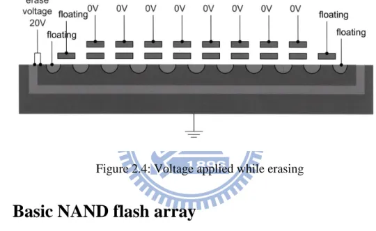
When NAND cell is being programmed, the selected word line is charged to 20V and all other cells shares the same bit line is charged to 10V, and then discharge bit line to 0V to perform a “0” programming. To erase the data in a block, the voltage of all word lines are discharged to 0V, and a 20V voltage is added on the source line to erase all cell to “1” therefore all pages that share the same source line must be erased at the same time. Figure 2.4 shows the array configuration while erasing.
Figure 2.4: Voltage applied while erasing
2.4
Basic NAND flash array
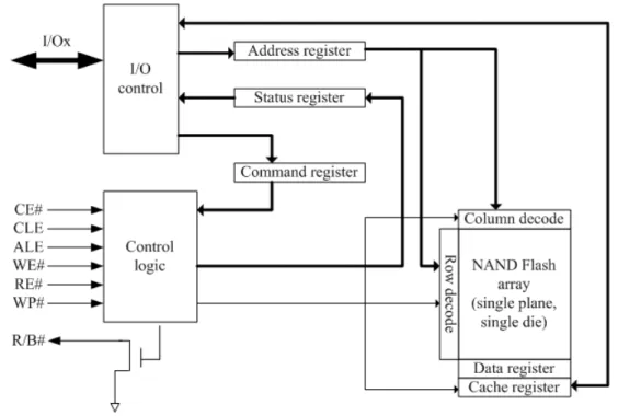
The array architecture of a basic NAND flash chip contains three functional blocks, which are I/O control, control logic and the NAND flash array.
NAND flash array includes all NAND flash cells and all column and row address decode multiplexers, the data to be programmed or the data read out from NAND flash are stored in data register and cache register. The traditional NAND flash cell array is organized as single plane, single die, so it only supports command which access one page at a time. NAND flash array uses two pages of register to maintain the ability to have a better performance of sequential access. I/O control logic controls the I/O signal of access,
I/O control relies on the status register which controlled by control logic to determine current I/O signal is a command, address or simply data to be transferred. The control logic receives input control signal to determine which action should be taken for I/O control and NAND flash array by the combinations of the input signals. Figure 2.5 shows the inner configuration of a NAND flash chip [7].
Figure 2.5: The NAND flash functional block diagram
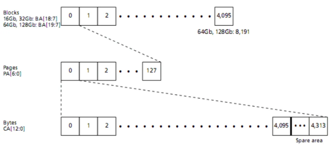
NAND flash does not contain dedicated address pins, therefore address are loaded using a five-cycle sequence. The detailed memory mapping and addressing are shown in Figure 2.6. The lower 13-bit are used to represent the column address of NAND flash
Figure 2.6: Memory mapping of a NAND flash chip
2.5
Advanced NAND flash array
The capacity of NAND flash device increases significantly as integrated circuit technique advances; the array organization of the NAND flash device also changes due to this capacity improvement. The inner architecture of an advanced NAND flash device is similar to a basic one but the NAND flash array is evolved to a multi-plane, multi-die one.
A multi-plane array packs more NAND cells on a same row entry, and separates it into different groups. When the row entry is selected, the data on this row can be accessed at the same time, so more than one page of data can be read/programmed with one flash array execution busy time, so the total access time can be saved. Figure 2.7 compares the basic NAND flash command with the advanced two-plane command. Multi-plane command must meet the address restriction: the command of two accesses must be the same, the page address of both commands must be identical and the least significant bit of the block address must be different [7], [8].
Figure 2.7: Comparison between basic command and two-plane command
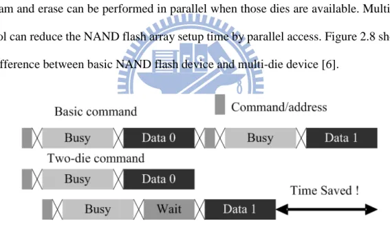
Multi-die array packs certain set of arrays together, each set of NAND flash array is like a basic one, but they share the same set of I/O signals. Basic commands like read, program and erase can be performed in parallel when those dies are available. Multi-die control can reduce the NAND flash array setup time by parallel access. Figure 2.8 shows the difference between basic NAND flash device and multi-die device [6].
Chapter 3
Functionalities of a Basic NAND Flash Controller
This chapter describes how a basic NAND flash controller works. Hardware architecture shows how NAND flash chips and controller are connected and the interface with higher level host.
3.1
System architecture of NAND flash chip
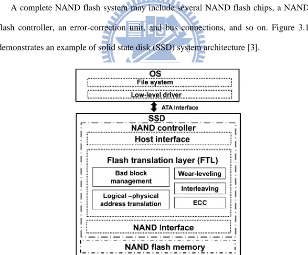
A complete NAND flash system may include several NAND flash chips, a NAND flash controller, an error-correction unit, and bus connections, and so on. Figure 3.1 demonstrates an example of solid state disk (SSD) system architecture [3].
The NAND flash controller receives command from host, and translates it into control signals accessing each NAND flash chip. Data reads out from NAND flash are sent to ECC unit to make sure the correctness of the desired information. Physical address translate block translates the virtual address from file system into the physical address that is being accessed [9]. Bad block management unit determines which block should not be accessed and how to deal with when the translated physical address is selected as a damaged block. Wear-leveling module dynamically changes the block to be programmed to make sure the write cycles of all good blocks are about the same.
3.2
The ONFi standard
Since the interface, addressing, device behavior of the NAND flash chips may differ by its vendor. The Open NAND Flash Interface (ONFi) tries to standardize all these specification to shorten the NAND flash system developing time [10]. The main philosophy of ONFi standard is described as below:
Ensure no pre-association with NAND flash at host design is required. All NAND flash parameters must self-describe through a parameter page; feature that cannot be self-describe shall be host discoverable, i.e. the number of CE#. ONFi should leverage existing NAND flash behavior to extent possible.
3.3
Basic command management
In order to control the NAND flash chip, four basic operations are required. Although the NAND flash array also supports some advanced command set like one time programmable (OTP) commands to perform data protection, these commands are seldom used and will not be introduce at this section.
Basic NAND flash commands include reset, read, program and erase. As mentioned in Section 2.3, NAND flash memory has to erase before a new data programmed, normal disk write command is divided into program and erase. Also by the architecture of the NAND flash array, more than one page is being erased while the minimum programming unit is one page. Therefore, sector based access will be a better choice for NAND flash file system.
Reset command is used to put the memory device into a known condition and to abort a command sequence in progress. Such command is used for simulation since the initial state of the NAND flash chip is unknown. The reset command clears all bytes in the NAND flash chip to 8’hff. Since all bytes are reset to an unprogrammed state, no other access address is needed. Controller sends command 8’hff and wait tRST for reset finished.
The ERASE command is used when another set of data needs to be programmed into a programmed page, old data must be erased before new data written. The erase command occurs at block level, and is operated at one block at a time. Since erasing is block aligned, only three cycles of address are required for a block erase operation, if a five-cycle address is transferred; only the last three cycles will be sent to the NAND flash chip. The actual command sequence is a two-step process. The ERASE SETUP (60h) command is first written to the command register. Then three cycles of address are written to the
device. Next, the ERASE CONFIRM (D0h) command is written to the command register. At the rising edge of WE#, R/B# goes low and the control logic automatically controls the timing of ERASE operation, R/B# stays low for tBERS for the entire erase time. Figure 3.4
shows the timing diagram of an ERASE operation [7].
Figure 3.2: Timing diagram of ERASE operation
The PROGRAM PAGE operation requires loading the SERIAL DATA INPUT (80h) command into the command register, followed by five address cycles, then the data. Serial data is loaded on consecutive WE# cycles starting at the given address. The PROGRAM (10h) command is written after input data loading is complete. The control logic automatically executes the proper algorithm and controls the entire timing program and verifies the operation. After tPROG, R/B# goes back to high and finishes the program
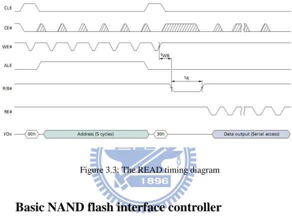
monitor the R/B# signal. After tR, the READ command can be re-issued, pulse RE# and
the data will output starting from the initial column address. Figure 3.5 shows the timing diagram of a READ operation [7].
Figure 3.3: The READ timing diagram
3.4
Basic NAND flash interface controller
The basic interface controller of a basic NAND flash device transfers an input command into corresponding control signal that controls the desired NAND flash chip. Each time one command is accessed since the basic NAND flash device can only access one page of data at a time. Under this control architecture, no command queues are needed and also I/O can share the same data buffer because data input/output won’t happen at the same time. The finite state machine of this interface controller is designed to suspend while NAND flash chip is executing; it simply ignores all requirements while execution.
Chapter 4
Proposed NAND Flash Controller
The proposed NAND flash controller architecture is introduced in this chapter. In order to achieve a higher operation speed, our proposed controller uses out-of-order (OOO) execution while commands in queues are independent. Also we use two-plane addressing to shorten the busy time of sequential data access. Controller uses OOO execution to enhance the ability of parallel access, meanwhile, in-order-commitment is used to simplify the protocol between host and controller.
4.1
Concept
The maximum performance that a NAND flash device can reach happens when the data transfer at a maximum rate with no chip busy waiting time needed. The minimum data transfer required cycle time of the NAND flash chip we use is 25ns, thus the maximum performance will be 40MB/s. In the following section, we introduce several ways to let the execution performance closer to the performance bound.
From the block diagram of the basic controller, all chips are connected to one interface control module, and only one command is accessed at a time. Therefore, only one small data buffer is needed while execution. The proposed controller use the sequencer to schedule parallel access cross chips, and the separate interface controller used two-plane command and distributed finite state machine is designed to improve the performance within a single chip; the I/O buffer of the controller also is separated into two sets to transfer input and output data at the same time. The proposed controller block diagram is shown at Figure 4.1.
The sequencer is designed to enhance the NAND flash device performance is to increase the probability of parallel access. For a basic NAND flash controller, only one interface controller is used, and control signal are set to each NAND flash chip through a de-multiplexer. Therefore, only one NAND flash chip is being accessed while other chips remain idle. For an advanced controller, a sequencer module is added to sense the probability of parallel access, and these commands are pre-loaded to other NAND flash chips to shorten the busy waiting time. Also, each NAND flash chip has its own interface controller to obtain the ability of parallel command controlling.
The interface controller extends its command set to shorten the average execution time of each access. A basic NAND flash controller uses only simple page read, program and erase commands. By the principal of locality, the data to be accessed are usually grouped together. The proposed NAND flash controller uses two-plane addressing and adds two-plane command set which can access two pages of data at a time. Thus the average data access time per page is cut down to half and the performance of the controller increases.
the same die must still access in-order. Only the command that access different dies may access in parallel when there is no data hazard.
For further hazard prevention, we discuss the four different scenarios that commands might appear in queues separately:
All commands in queues are all read type instructions. All commands in queues are all write type instructions. Write type commands follow by read.
Read type commands followed by write.
When all commands in queues are all read type commands, no data hazard will occur since there is no read after read (RAR) hazard. The execution order of read commands won’t affect the result of each data reads out from NAND flash. Therefore the read command of an idle chip can be sent first to shorten the data waiting time by increasing the number of parallel accesses among chips.
If the commands in queues are write-type, the data in NAND flash device may change after each write, so we must ensure that the data written to NAND flash chip is in the correct order. In order to avoid all data hazards, first we need to know the data dependency between commands. Write after write (WAW) hazard happens when the address of two write accesses are the same, so all these commands need to be executed in order. For simplicity, controller performs only chip and die address bit comparison to reduce the area of comparator, commands that access the same die are executed in order. Because the minimum execution unit is one die, there will be no performance lost if we
only compare the chip and die address bit. All commands that want to write to different dies can be executed in parallel to increase the performance.
For write-type commands that followed by read-type commands (RAW), the situation is similar to a WAW scenario. If both read and write commands are going to access the same page/block, the write-type commands must finish before data is read out. All write-type commands that must finish before the read type commands are on the same die, therefore commands that do not access the same die can be executed in parallel. Sequencer design is the same as the former configuration.
The last condition is write after read (WAR) hazard. In order to prevent this hazard, we shall explore the data dependency at this condition. Same as before, if the read type command and the write type command are going to access the same die, all read must be done before write happens, and the operation is the same as previous conditions. But, unlike those three conditions, read occurs at other dies also need to finish before write type command to ensure the data that writes into the NAND flash chip is correct. Figure 4.2 shows an example that write type commands on a different die needs to wait before read finish. First, it appears that we only need to ensure that the command which desired to access the same die must be executed in-order, so in Figure 4.2, the first, third, forth
Figure 4.2: Example of WAR prevention
For all these four situations above, only write after read needs further control logic to prevent data hazard; for other three situations, sequencer only needs to ensure that commands executed in each die are in order. Therefore for a sequencer to adapt all conditions, it simply halts all write after read until read type commands finish; otherwise the commands in queues are executed in parallel if the chip and die address are different from each other.
4.3
In-order commitment
The proposed NAND flash controller enables out-of-order execution; therefore the finish time of each command will also be out-of-order. However, in-order commitment is used to simplify the interface between host and controller since out-of-order commitment requires more interface handshaking and will increase the complexity of error handling, (e.g., interrupts).
All commands in queues are sent to the NAND flash chip in parallel to shorten the command setup time. After the executing command finished waiting, it is halt until all previous commands are committed. Figure 4.3 demonstrates an example of in-order commitment. Although the read command sent to chip 2 and chip 3 are ready for data transfer, they must wait until the command required to write chip 1 is finished and then start the data transfer.
Figure 4.3: The example of in-order commitment
locality, the address of command in queues are going to access is not far from each other, so it is hard for the controller to find two commands which can apply the two-plane commands from the command queue. Even though the controller finds commands that can apply two-plane commands, the in-order commitment made controller difficult to handle those situation efficiently. If we want to gain the advantage of two-plane command set, we must change the addressing mode to adapt the property of two-plane commands.
Figure 4.4 shows the comparison between two-plane addressing mode and the original one. Our proposed NAND flash controller left rotates the page address by one bit and thus changes the position of the LSB of the block address bit. This step is done by each interface controller before sending the address to the NAND flash device. Therefore the flash transfer layer still sees the same address as the original one. After this address transformation, every two sequential accesses naturally form a two-plane command and it is easy for controller to handle this change by introducing an extra sequential valid bit to tell the controller when to apply these two-plane commands.
Figure 4.4: Comparison between original and two-plane addressing mode
4.5
Interleaved command
Interleaved commands are used when dies in each NAND flash chip were idle. The interleaved commands act as the normal one, so the sequencer considers each die as a independent chip and does not need further comparison logic. In order to obtain the ability of interleaved access, the interface controller must made command input of idle dies possible while some other dies are during execution. The basic interface controller access one command at a time, so the chip finite state machine simply waits while NAND
Since interleaved command may occur when read command busy time, the interface controller need to inform the NAND flash chip which die is being accessed before the normal commands. Figure 4.5 shows an example of status monitoring for an interleaved page read command [7]. A status monitoring command 78h must sent to the NAND flash chip to inform the devices which die are going to be accessed for the correctness of the command. The interface controller is designed to send the address information to the NAND flash chip for all accesses even if the interleaved command is not activated to simplify the control logic. For erase and program commands, the command finish when the command/address/data transfer completes. Therefore we only need to ensure that the die finished execution before sending the next command to the die being accessed. The status monitoring command for erase and program will be optional and the controller simply skips that to reduce the complexity of the sequencer.
4.6
Conclusions
Our proposed NAND flash controller tries to improve the execution performance by enhancing the ability of parallel access and by reducing the average data access time per page.
The sequencer of the proposed NAND flash controller determines when the commands in command queue can be accessed in parallel while avoiding all data hazards and sends them to all interface controllers. The interface controller uses distributed finite state machine design to make interleaved command execution possible. Both sequencer and interface controller are designed to enable more commands to be accessed in parallel to improve performance.
The average access time per page is reduced by introducing the two-plane addressing mode. The interface controller automatically changes the page address of each command before sending it to the NAND flash chip. The flash transfer layer still sees a sequential address but every two commands automatically form a two-plane command to save data access setup time.
By the two methods above, our proposed NAND flash controller can improve the performance of command execution and the detailed comparison between the basic and
Chapter 5
Experimental Results
In this chapter, we demonstrate the ideal performance of a single NAND flash chip and show the experimental result of the basic and proposed NAND flash controller. Also, the comparison between the two NAND flash controllers is shown in this chapter.
5.1
Ideal Performance of commands
The performance of basic commands are determined by the data transfer time and the R/B# low waiting time. Table 5.1 shows the timing parameters of each type of access [7].
Table 5.1: Timing characteristic of different access
Parameter Symbol Min. Typ. Max. Unit
READ cycle time tRC 25 - - ns
RESET time tRST - - 5 μs
BLOCK ERASE operation time tBERS - 3.5 10 ms
PROGRAM PAGE operation time tPROG - 900 2200 μs
Data transfer from NAND flash array to
data register tR - - 50 μs
Data transfer time per page tD 107.85 - - μs
The minimum READ cycle time determines the minimum cycle time of the NAND flash controller, so the cycle time of the NAND flash controller will be 25/2=12.5ns. The address time and command time are 125/25ns, separately. Since the data transfer time and R/B# waiting time are significantly larger than the command time and address time, we
abbreviate the command time and address time to simplify the computation of NAND flash performance.
The execution time of an ideal NAND flash controller is simplified as the formula below by neglecting all command and address transfer time:
low R/B# D inst =t +t t
Thus the performance of all commands can be calculated by the equation:
low # B / R D+t t size data total = e performanc ideal
The ideal performance of each command is shown in Table 5.2. The performance is evaluated under a single die execution case and the maximum performance happens when the buffer transfers data at maximum rate.
Table 5.2: The ideal performance of NAND flash commands at a single die Instruction Type Ideal Performance (MB/s)
Max. performance 40 Read 26.1 Two-Plane Read 31 Program 4.1 Two-Plane Program 7.4 Erase 150.5
5.2
Experiment setup
Figure 5.1 shows the experiment setup. A virtual flash transfer layer sends the target physical address and the relative command to the proposed NAND flash controller; the controller is connected to four identical NAND flash devices.
Figure 5.1: The experiment setup of the NAND interface
The starting address of each scenario is generated randomly. Four scenarios of input commands are tested to measure the performance of the NAND flash controller:
Sequential read Random read Sequential program Random program
5.3
EDA environment and synthesis result
Table 5.3 shows the EDA tools used for simulation and synthesis.
Table 5.3: The EDA environment used for experiments
Frequency 80MHz
Simulator Cadence NC-Verilog Technology TSMC 0.18um
Synthesis Synopsis Design Compiler
The synthesis frequency is determined by the minimum read cycle time to achieve the maximum performance of the NAND flash controller. The properties of our proposed NAND flash controller are described as below:
Four interface channels. Eight command queue entries.
The synthesis result of both basic and proposed controller is reported as below, the area is shown by NAND-2 equivalent gate count:
and command queue enhanced the ability of out-of-order execution at the expense of increase in area of the proposed controller.
5.4
NAND Flash simulation model
Table 5.4 shows the NAND flash simulation model and its properties that we use to connect to the NAND flash controller.
Table 5.4: The properties of the NAND flash model used for simulation
Simulation model Micron MT29F32G08Q
Chip size 32Gb
Block size 128 pages
Page size 4314 bytes
Chip organization 2 planes, 2 dies
5.5
Experimental Results
Table 5.5 shows the sequential read performance comparison between the basic controller and the proposed controller. Since the basic controller only accesses one page at a time, the access length of the sequential read command does not affect the performance. Alternatively, our proposed controller improves the performance majorly by using the two-plane read command; the improvement is independent of access length because out-of-order execution may only happen when each set of sequential read access is finished.
Table 5.5: Experimental result of sequential read
Access Length (Blocks) 1 2 4 8
Basic (MB/s) 25.99 25.99 25.99 25.99
Proposed (MB/s) 30.84 30.79 30.78 30.77
Improvement 18.6% 18.5% 18.4% 18.4%
The experimental result of random read is shown in Table 5.6. The performance of the basic controller is identical to the sequential one since the access length is independent of the command set that the basic controller uses. A significant performance improvement of the proposed controller comes from the out-of-order execution between chips and dies for random read that only access one page at a time. Another 4.3% of improvement for the access length of sequential read increase from 1 page to 2 pages due to the usage of two-plane command. The performance drops from 2 pages to 16 pages because of the frequency that commands can be executed in parallel decreases due to the increment of the access length.
Table 5.6: Experimental result of random read
Access Length (Pages) 1 2 4 8 16
Basic (MB/s) 25.99 25.99 25.99 25.99 25.99 Proposed (MB/s) 35.7 36.83 33.52 32.09 31.41
performance is close to the ideal performance of a program command. The performance of the proposed controller is close to the ideal two-plane program command, but it has a greater improvement when the access length is smaller since there might be out-of-order execution between each set of sequential access. Sequential program has a better performance improvement than sequential read because the NAND flash busy time of program is longer than the data transfer time whereas it is shorter for a sequential read. The program command thus gains a better command parallelism so it has a higher performance improvement.
Table 5.7: Experimental result of sequential program
Access Length (Blocks) 2 4 8
Basic (MB/s) 4.02 4.02 4.02
Proposed (MB/s) 7.67 7.46 7.36
Improvement 90.9% 85.7% 83.2%
Table 5.8 shows the experimental result of random program. Although the access length of random program is less than one block, all data in the selected block must be erased before each program access due to the NAND flash program property. The frequency that the erase command is needed before program decrease as the access length increases. Therefore the performance becomes better as the access length increases for the basic NAND flash controller. The proposed NAND flash controller enhances the performance by out-of-order execution and two-plane command, but its performance is also affected by the performance drop of the erase command. The proposed controller has the best performance when the access length is 8 pages, and the performance decreases slightly as access length increases.
Table 5.8: Experimental result of random program
Access Length (Pages) 2 4 8 16 32
Basic (MB/s) 2.05 2.73 3.27 3.63 3.84
Proposed (MB/s) 9.59 11.59 12.47 11.51 10.8 Improvement 3.68x 3.25x 2.81x 2.17x 1.81x Comparing the performance of basic and proposed controller, we can see that the performance improvement decrease as the access length increases since we eliminate the effect of the erase command, which is a performance decreasing factor. The decrease of the performance comes from the frequency drop of the out-of-order execution as the access length increase.
From the experimental results above, we can see that the proposed controller outperforms the basic controller in all kinds of access. For sequential data access, the performance improvement is close to the improvement from single-plane command to a two-plane command. For random data access, it has a better improvement due to the ability of out-of-order execution; the improvement also drops as the access length increases since the frequency of the out-of-order execution decreases.
Chapter 6
Conclusions and Future Works
A high-performance NAND flash controller design is proposed in this thesis. The proposed NAND flash controller features out-of-order execution to improve the performance. The sequencer determines the out-of-order execution order by the two principals: the commands that desired to access the same dies are executed in-order and all the read commands before write commands must be finished first to avoid the potential WAR hazard. The interface controller changes the address of that commands required to access into two-plane addressing mode to improve the average access time per page by using two-plane commands.
The experimental results show that the proposed high-performance NAND flash controller can improve the performance of the four kinds of execution as follow:
Up to 18.6% for sequential read. Up to 41.7% for random read. Up to 90.9% for sequential program. Up to 3.68x for random program.
We will try to further enhance the performance by multi-channel data transfer between host and the NAND flash controller in the future.
References
[1] S. H. Lim and K. H. Park, "An efficient NAND flash file system for flash memory storage," In IEEE Transactions on Computers, vol.55, no.7, pp. 906-912, Jul. 2006.
[2] R. Bez, E. Camerlenghi, A. Modelli and A. Visconti, "Introduction to Flash Memory," In
Proceedings of the IEEE, vol.91, no.4, pp. 489-502, Apr. 2003.
[3] K. Takeuchi, “Novel Co-Design of NAND Flash Memory and NAND Flash Controller Circuit for Sub-30 nm Low-Power High Speed Solid-State Drives(SSD),” In IEEE Journal
of Solid-State Circuit, volume 44, pp. 1227-1234, Apr. 2009.
[4] International Technology Roadmap for Semiconductor, 2007.
[5] S. L. Min and E. H. Nam, “Current trends in flash memory technology,” In Asia and South
Pacific Conference on Design Automation, pp. 332-333, Jan. 2006.
[6] C. Park, P. Talawar, D. Won, M. Jung, J. Im, S. Kim and Y. Choi, “A High Performance Controller for NAND Flash-based Solid State Disk(NSSD),” In IEEE NVSMW Non-Volatile
Semiconductor Memory Workshop, pp. 17-20, 12-16, Feb. 2006.
[7] Micron Technology Inc., “Mass Storage: MT29F32G08QAAWP,” May 2008. Available: http://www.micron.com/products/partdetail?part=MT29F32G08QAAWP.
[10] ONFi, “Specifications,” Nov. 2007. Available: http://onfi.org/specifications/.
[11] J.L. Hennessy and D.A. Patterson, Computer architecture: a quantitative approach, 4th edition, Morgan Kaufman Publishers, 2007.
[12] C. S. Lin, K. Y. Chen, Y. H. Wang and L. R. Dung, "A NAND Flash Memory Controller for SD/MMC Flash Memory Card," In IEEE International Conference on Electronics, Circuits
![Figure 2.1 shows the transistor configuration of a single flash cell [2]. By adding the floating gate into a traditional MOSFET, flash cell uses Flowler-Nordheim (FN) tunneling to drive stored electrons to memorize data after power off](https://thumb-ap.123doks.com/thumbv2/9libinfo/8761577.208309/13.892.136.773.525.956/transistor-configuration-floating-traditional-flowler-nordheim-tunneling-electrons.webp)