A One-Transistor Synapse Circuit with an Analog LMS
Adaptive Feedback
for
Neural Network VLSI
T. C. Lu, M. L. Chiang and J. B. Kuo
Rm. 526, Uept. of Electrical Eng., Xa-ational Taiwan University
Roosevelt Rd. Sec. 4,
#1,
Taipei, Taiwan
FAX:886-2-363-8247,
Telephone:886-2-363-5251,
E-mail:t7503007@twntuccl.
bitnet
Abstract
Current integrated circuits realizing neural networks consume too much area for implementing synapses. This paper presents a one- transistor( 1T) synapse circuit, which uses a single MOS transistor, more efficient for VLSI implementation of adaptive neural networks, as compared to other synapse circuits. This 1T synapse circuit can be used t o implement multiply/divide/sum circuits for realizing an adaptive neural network. The feasibility of using this circuit in adap- tive neural networks is demonstrated by a 4-bit analog-t- digital converter circuit based on the Hopfield’s modified neural network model with an analog LMS adaptive feedback. DC and transient study shows that the 1T synapse circuits with an analog adaptive feedback circuit can be more efficiently used for VLSI implementa- tion of adaptive neural networks.
1.Introduction
Recently, VLSI implementation of neural networks [1],[2] receives widespread attention owing to better speed performance for the model realized by hardware compared t o by software. In most neural net- work ICs, most of the chip area is occupied by a large number of complicated synaptic connections. For example, Graql] uses four switches and two resistors to construct a synapse and nearly 90% of the chip area is occupied by the synapses. Although in other applications[2]-[5], simpler synapse circuits have been proposed, they are not concise enough for efficient VLSI implementation. It bas been pointed out that the number of neurons in a chip determines the the storage capacity of a neural network no matter what learning rules have been used[6]. In reality, the number of neurons can be placed in a N N chip is limited by the size of the synaptic connections area. How to reduce the size of the synapse circuits bas been the major task in designing neural network ICs. In this paper, a concise synapse circuit using a single MOS transitor will be described. It will also be shown that the multiply/divide/sum circuit implemented with this 1 T synapse circuit has a good linearity within the output dynamic range for the neural networks with an analog adaptive feed- back circuit. The feasibility of using this 1T synapse circuit will be demonstrated by a 4-bit analog-t-digital converter circuit using the Hopfield’s modified neural network model[7] with an LMS adaptive feedback.
11. The Multiply/Divide/Sum Circuit
In Hopfield’s modified neural network model, a neuron performs a sigmoid function of its input, which is the summation of other neu- rons’ outputs multiplied by the weights stored in the synapsts. Many synapse circuits have been proposed and implemented. Until now, the synapse circuit realized by a resistor is the most efficient. However, realization of a large amount of resistors requires special processing technologies[8]. Fundamentally, the resistor synapse serves as a role to transform the output voltage of one neuron’s output t o an input current for another neuron with a weight. Here, a single MOS tran- sistor with a zero threshold voltage, which can be easily realized by adjusting the doses of the channel implants in a CMOS fabrication process, operating in the triode region has been used t o replace the resistor for the synapse circuit. This 1T MOS synapse circuit per- f o r m as a programmable resistor with its conductance determined by the W/L ratio and the gate voltage. Figure 1 shows the multi- ply/divide circuit built with the 1T synapse circuits. With an NMOS synapse circuit a t the input and a PMOS one in the feedback path, the circuit provides a good linearity property for multiply/divide op- erations. Figure 2 shows the SPICE simulated characteristics of the multiply and the divide operations. For one input, x, with a swing between - l V and + l V and another input, y, with a positive swing and the other input, z , with a negative swing, the output, v,, = kxy/z, has a swing from - l V t o 1V. Within the output dynamic range, both the multiply and divide operations have an acceptable linearity for adaptive neural network applications.
III.The Analog Adaptive Circuit
Adaptation has been broadly used in signal processing, control and telecommunication systems t o remove non-ideal effects [9]. The adaptive circuit in neural networks is used t o compensate for the 1T synapse circuits and the neuron circuit with non-zero thresh- olds. Usually, adaptive neural networks, proposed in trainable pat- tern recognition [lo], are realized by either computer software or dig- ital circuits with analog-to-digital and digital-to-analog conversions required. During the training period, many iterations are required for convergence of the weight functions, which determine the conduc- tances of the synapses [SI. This d a t a conversion requirements severely limit not only the complexity of the patterns can be trained but also the storage capacity of the neural networks. Fig. 3 shows an ana, log adaptive feedback circuit. This analog adaptive circuit is derived from the digital LMS algorithm [9]: w k + 1 = wk
+
$$,ox, where wk+lis the next value of the weight vector, wk is the current value of the weight vector, X k is the current input vector, cr is a parameter to adjust, and c k is the error, which is defined as the difference between the desired output and the analog output [9].
-~ .___-
The transistor MN1 is a synapse circuit with the source end con- nected t o the input -I and the gate controlled by the weight function
w . With the -d conncected to the positive input, tlie op amp O A l
produces the error which is the difference between the tlie desired output, d and the product of the input and the weight. Then the error is integrated through the OA2 circuit as the new weight for the synapse circuit. During t h e training period, the switch SW is on and the weight w converges to a value such that I W = d. Based on the
analog adaptive feedback circuit, the weight function is written as:
w ( t ) = w 0
+
p o / * ( i - R [ ( w+
2)z - ---I)& 1 x 2O P
2 PPo = 5@op/c
where W O is the initial value of the weight vector, w(t), ~ ( t ) are the current values of the weight, the input respectively.
pa, 0
are tlie beta for the transistors MNO, M N 1 respectively, and C is tlie inte- grator capacitor. Fig. 4 shows the SPICE simulation results of tlie weight and the percentage error in terms of the maximum error dur- ing the training period, of the analog adaptive circuit designed for two different P O ’ S , which are determined by the corresponding circuit parameters. A larger PO results in a quicker response. However, a larger /I may also leads to instability. Generally speaking, in spite of the nonlinearity of tlie adaptive circuit, the weight converges to its final value within a few microseconds [ll]. Fig. 5 shows the available swings of the input I and the weight for different desired outputs, d .A
smaller d provides a larger swings a t the input and the weight. For the neural net applications, the available swings a t tlie input and tlie weight are sufficient for circuit design.IV.The ADC Circuit
In order t o show the applicability of the 1T synapse circuit, with the analog adaptive feedback, a 4-bit ADC circuit using Hopfield’s modified neural network model [7], [12] has been implemented with the 1T synapse circuits as shown in Fig. 6. P-channel and N-channel
MOS
devices with a zero threshold voltage have been used in the synapse array. In fact, the synapse array can still work with MOS devices having non-zero threshold voltages for the ADC with the ana- log adaptive feedback.The conductance zj of each synapse circuit is determined by tlie for- mulasdescribed below. Tzi
= C G 2 ’
,
T i j= C&-2’+J , TR,
= C k 2 ‘,
where VBB is the swing of the neuron output, VH is the swing of the inputI,
and N is the number of bits.With a 5V supply connected to all gates, the synapse circuits can be programmed by properly choosing the W / L ratios for their spec- ified T’s. Fig. 7 shows the layout of the synapses array based oil a
2pm, 1-layer metal, 1-layer poly, N-well CMOS process, for t.he ADC using adaptive nerual net. The
Zj’s
synapses are permut,ed vert.ically from left to right, followed by the TR,’s and the Tx,’s. Power sup- plies of V s s and VDD are connected from tlie bottom riglit. Inputs ofthe synapses are from the left, Vo, V I , Vz, V3, which are t.lie neuron outputs. The ouputs of the synapse array are 210, U ] , U ? , u s , at the right. Input signal, I , and reference voltage,
-VR,
are also from t.lieright. The hatch area shows the polysilicon layer, wliich is used for gates of the synapses and cross-overs. The synapse array occupies a silicon area of 140pm x 140pm. Overall layout of the synapse array is simple and efficient, which shows the strength of tlie 1 T synapse circuit for neural net VLSI.
The neuron performing a sigmoid function with a la.rge gain is re- alized by the CMOS op amp with an output stage served as a level shifter and an output drive as shown in Fig. 8(a). The small signal dc gain of the neuron circuit is about, 5000, which is high enough such that the energy maxima and minima locate at the corners of the hypercube where all the neuron outputs are ” 0 ’ and ”1” exact,ly
[13]. The compensa.tion capacitor C c of 2pF is used t,o provide a sta-
ble frequency response. The unity gain bandwidth product is about
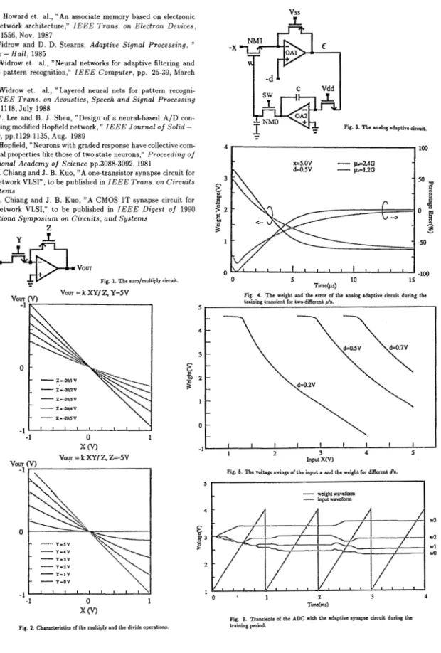
2 M H z . Fig. 8 (b) shows the layout of the neuron circuit. It oc- cupies a silicon area of 200pm x 240pm. The power dissipation of the neuron ciruit is about 2mW. Due to the variations during the fabrication process, the neuron circuit may have an un-predictable non-zero threshold voltage, whose effects can be removed by adjust- ing the weights of the synapses connected between the input of the neuron and the reference voltage -VR controlled by the adaptive cir- cuit during the adaptation period [14], [15].
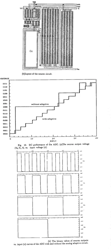
Figs. 9 and 10 show the transients of the ADC with the adaptive 1T synapse circuit during the training period. As shown in Fig. 9, initially, the synapse weights are set a t 3V. When is the adaptation is on, switches SWo-SW3 are closed, a repetitive training pattern of a linearly increasing waveform is imposed a t the input I. The adapt strategy used here is to adjust the T’i’s of four bits such that the nonideal effects associated with the neuron circuits can be reduced and the ADC characteristics for the overall input swing can be op- timized. After four reptitions of the input pattern, the four weights associated with synapses Tx0, Txl,
Txz,
Tx3 converge to their final values. Then, switches SWO - S W 3 are open, and the A/D converter begins to work with the adapted conductances stored in t,he capaci- tors CO - C3.Fig. 10 shows the dc performance of the ADC with tlie adaptive 1T synapse circuit. Fig. 10 (a) show the neuron output voltages (Vo, V I , Vz) vs. input (V,”) curves a t dc for output swings from 0 to -5V and from 0 to - l V respectively. The resolution of the A/D converter with the analog adaptive circuit within the input dynamic range (0-4V) is much more uniform as compared to the ADC with- out it. Fig. 10 (b) shows the binary values of neuron outputs vs. input ( x ) curves with and without the analog adaptive mechanism. Without the adaptive feedback circuit, the 4-bits ADC with the 1 T synapse circuits show an unacceptable performance. With the adap- tive feedback, the 1 / 0 transfer characteristics are linear.
So far, the adapt,ation of synapses for removing tlie noli-zero neuron offsets has been considered. In fact, the nonlinearity in the conduc- tance of the MOS transistor and the non-ideal neuron outputs, which affects tlie T,,’s, can be critical in the performance of the neural nets, too. Consequently, the TiJ’s need also be trained individually. We may expand the adaptation period to cover the individual training of each synapses other than offset correction related synapses. VI. References
[l] H. P. Graf, L. D. Jackel, and W. E. Hubbard, ”VLSI implementa- tion of a neural uet.work model,” I E E E Computer pp.41-49, hlarch
1988
[2] M. Verleysen, et.. al.,”A high-storage capacity content-addressable memory and its learning algorithm,” I E E E T r a n s . 07) Circuits a n d Systems, pp.762-766, May 1989
[3] M . Verleysen, et. al., ”Neural networks for high-st,orage content addressable memory: VLSI circuit and learning algorithnl,” I E E E
J o u r n a l of Solid - S t a t e Circuits, pp.562-569, J u n e 1989 [4] K. A. Boahen, et. al., ” A heteroassociative memory using current- mode MOS analog VLSI circuits,” I E E E T r a n s . on Circuits a n d Systems, pp.747-755, May 1989
[5] R. D. Reed and R. L. Geiger, ”A multiple-input OTA circuit for neural networks,” I E E E T r a n s . on Circuits and S y s t e m s . pp.767- 770, May 1989
[6] R. P. Lippman, ”An introduction to computing with neural nets,”
I E E E A S S P Maga:ine, April 1987
[7] D. W . Tank and J . J . Hopfield, ”Simple neural optimization net- works: An A/D converter, signal decision circuit, and a linear pr-
gramming circuit,” I E E E T r a n s . on Circuits and S y s t e m s , pp.533- 541, May 1986
[8]
R. E.
Howard et. al., ”An associate memory based on electronic neural network architecture,” IEEE T r a n s . on Electron Devices, pp.1553-1556, Nov. 1987[9]
B.
Widrow andD.
D. Stearns, Adaptive Signal Processing, ” Prentice - H a l l , 1985[lo] B. Widrow et. al., ”Neural networks for adaptive filtering and adaptive pattern recognition,” IEEE Computer, pp. 25-39, March 1988
(111 B. Widrow et. al., ”Layered neural nets for pattern recogni- tion,” IEEE T r a n s . on Acoustics, Speech a n d Signal Processing [12]B. W. Lee and B. J . Sheu, ”Design of a neural-based A/D con- verter using modified Hopfield network, ” IEEE J o u r n a l of Solid - Circuits, pp.1129-1135, Aug. 1989
[13]J. J . Hopfield, ”Neurons with graded response have collective com- putational properties like those of two state neurons,” Proceeding of the National Academy of Science pp.30883092, 1981
[14]M. L. Chiang and J . B. Kuo, ” A one-transistor synapse circuit for neural network VLSI”, to be published in IEEE T r a n s . on Circuits a n d Systems
[15]M. L. Chiang and J . B. Kuo, ” A CMOS 1T synapse circuit for neural network VLSI,” to be published in IEEE Digest of 1990 Internationa Symposium on Circuits, a n d Systems
pp.1109-1118, July 1988
Z
Vom
Fig. 1. The sum/multiply circuit.
-1
0
1x
(VI
Fig. 2. Characteristics of the multiply and the divide operations.
VSS
-xykjpi
100 4 p 2 A G x=5.OV-
d=OSV-
P U G j 5 0Fig. 4. The weight and the error of the analog adaptive circuit during the training transient for two different p’s.
5 1
11 1 I I I 1 I I I I
1 2 3 4 5
Input
XW)
Fig. 5. The voltage swings of the input I and the weight for different d’a.
’ 1
1
t
423
P
2 1 0-
weight waveform-
input waveform w3 UR w l WO 1 2 3 Time(ms)Fig. 9. Tkansientr of the ADC with the adaptive synapse circuit during the training period.
4
' T
Fig. 6. The 4 b i t ADC circuit using Hopfield's modified neural net model
...
I.:, ,I.- _ _ _ I ^ _ -A-..:...- ...--I.-- :--1
n r r
1 m
l x
Fig. 7. Layaut'of the synapse array for the ADC using adaptive neural net VDU
V V V vss
(b)Layout of the neuron circuit.
OUTPUT 1111 1110 1101 I 1 0 0 1011 1030 1001 without adaptive
-
-
- --
-
-
0111 0110 0101 0100 --
-
-
I , . , , I t * a . I . I . ' 0 1V 2v 3v 4v(b)Layout of the neuron circuit
OUTPUT 1111 1110 1101 I 1 0 0 1011 1030 1001 without adaptive
-
-
- --
-
-
0111 0110 0101 0100 --
-
-
I , . , , I t * a . I . I . ' 0 1V 2v 3v 4v mLTFig. 10. DC performance of the ADC. (a)Thc neuron output voltage ( ~ , V l , V z YS. input voltage (2).
(b) The binary values of neuron Outputs and without the analog adaptive circuit.
YS. input (z) curves the ADC
Fig. 8. (=)The neuron circuit.