Selective growth of single InAs quantum dots using strain engineering
B. C. Lee, S. D. Lin, C. P. Lee, H. M. Lee, J. C. Wu, and K. W. Sun
Citation: Applied Physics Letters 80, 326 (2002); doi: 10.1063/1.1433169 View online: http://dx.doi.org/10.1063/1.1433169
View Table of Contents: http://scitation.aip.org/content/aip/journal/apl/80/2?ver=pdfcov
Published by the AIP Publishing
Articles you may be interested in
Single InAs quantum dot coupled to different “environments” in one wafer for quantum photonics
Appl. Phys. Lett. 102, 201103 (2013); 10.1063/1.4807502
RHEED transients during InAs quantum dot growth by MBE
J. Vac. Sci. Technol. B 30, 02B128 (2012); 10.1116/1.3694019
Growth and characterization of Si-doped self-assembled InAs quantum dots
J. Vac. Sci. Technol. B 23, 1047 (2005); 10.1116/1.1900735
Selective growth of InAs quantum dots on patterned GaAs
J. Vac. Sci. Technol. B 23, 262 (2005); 10.1116/1.1856464
Area-controlled growth of InAs quantum dots and improvement of density and size distribution
Appl. Phys. Lett. 77, 3382 (2000); 10.1063/1.1327613
This article is copyrighted as indicated in the article. Reuse of AIP content is subject to the terms at: http://scitation.aip.org/termsconditions. Downloaded to IP: 140.113.38.11 On: Thu, 01 May 2014 06:27:55
Selective growth of single InAs quantum dots using strain engineering
B. C. Lee, S. D. Lin, and C. P. Leea)Department of Electronic Engineering, National Chiao Tung University, Hsinchu, Taiwan, Republic of China
H. M. Lee and J. C. Wu
Department of Physics, National Changhua University of Education, Changhua, Taiwan, Republic of China K. W. Sun
Department of Physics, National Don Hwa University, Hualien, Taiwan, Republic of China
共Received 31 July 2001; accepted for publication 5 November 2001兲
A method to achieve ordering and selective positioning of single InAs self-assembled quantum dots
共QDs兲 has been developed. The selective growth was achieved by manipulating the strain
distribution on the sample surface. The QDs are formed on predesigned mesas with added strain. Single dots were obtained on small mesas. Using this technique, two-dimensional single QD arrays have been achieved. © 2002 American Institute of Physics. 关DOI: 10.1063/1.1433169兴
The self-assembled quantum dots 共QDs兲 grown by Stranski–Krastanov共SK兲 mode are promising candidates for use in quantum devices because of their ease in fabrication and their high-quality, defect-free properties. Device applica-tions using QDs, such as QD lasers,1QD resonant tunneling devices,2and memory devices,3 have been intensively stud-ied for several years. However, QDs grown using SK growth mode are usually randomly distributed on the growth surface and suffer from fluctuations in size and strain in a random manner. It is almost impossible to place QDs in a organized way and at predesigned locations. The size fluctuation also results in large inhomogeneous broadening in their energy spectrum. This seriously limits potential-device applications of the QDs.
Recently, in order to solve these problems, there has been a great amount of effort expended in the study of self-assembled QD formation on patterned substrates to improve control of the size uniformity and position. Mui et al. made use of differences in atom diffusion on faceted surfaces to control QDs formation.4 Lee et al. combined lithography with in situ lateral strain engineering to control QDs formed on a mesoscopic surface.5 Tsui et al. utilized selective area epitaxy and an oxide-patterned substrate to position QDs on a GaAs facet.6As for fabrication of single QDs, recent stud-ies have demonstrated site control of individual QDs by in situ nanolithography combined with molecular beam epitaxy using an ultrahigh-vacuum multichamber system.7,8 But the main problems they are confronted with are direct QD growth on the etched surface, unknown materials introduced during the patterning process, and a complex multichamber system.
In this letter, we report a selective growth method that is capable of placing a single InAs QD at a given location on a GaAs substrate. The idea behind this technique comes from the following:共1兲 self-assembled QDs are formed because of strain relaxation during dot formation and result in a de-crease in the total strain energy of the epilayer/substrate
sys-tem, and 共2兲 if a local strain is artificially introduced into a given region, a two-dimensional 共2D兲-to-three-dimensional
共3D兲 morphology change will take place before a critical
thickness 关c⬃1.57 monolayer 共ML兲兴 is reached for InAs QD formation. In our method, selective growth of QDs is achieved by artificially introducing additional strain energy at certain predesigned locations that are defined by e-beam lithography. QDs are therefore grown only at the locations selected while in other regions only 2D growth takes place. We have demonstrated single QD formation on small e-beam defined mesas. Controlled single dot arrays have also been achieved using this technique.
Our experiment was carried out in a Varian Gen II mo-lecular beam epitaxy共MBE兲 system using As2共cracked As4兲
as the arsenic source. Figure 1 illustrates the sequence of our selective growth technique. First, in order to obtain local strain distribution, we deposited a 100 Å In0.2Ga0.8As layer
and a 200 Å GaAs capping layer on an epi-ready GaAs共001兲 substrate. The substrate was then coated with 2% PMMA, and exposed to an e-beam to define a square lattice of mesas. The linear dimension of each mesa was 200 nm⫻200 nm, and the mesas were separated by 500 nm. After PMMA development and wet chemical etching in a H2SO4:H2O2:H2O⫽1:8:80 solution, the patterns were
transferred onto the GaAs substrate. The etched mesas have a height of about 500 Å.
Before being introduced into the MBE system, the pat-terned GaAs共001兲 substrate was cleaned in solvent and then about 100 Å GaAs was removed by wet chemical etching using a H3PO4:H2O2:H2O⫽3:1:50 solution. The MBE re-growth started with oxide desorption under As2 flux at 610 °C. After the oxide layer was desorbed, the substrate temperature was lowered to 510 °C to deposit an 80 Å In0.1Ga0.9As buffer layer, which was used as a strain fine-tuning layer on the surface. This layer increases the strain energy to ensure subsequent QD formation on the mesas. Finally, 1.35 ML of InAs was deposited at a growth rate of
⬃0.05 ML/s and a V/III beam equivalent pressure ratio of ⬃100. The sample was cooled down under As2 flux
imme-diately afterward. While 1.35 ML of InAs is not enough to a兲Electronic mail: [email protected]
APPLIED PHYSICS LETTERS VOLUME 80, NUMBER 2 14 JANUARY 2002
326
0003-6951/2002/80(2)/326/3/$19.00 © 2002 American Institute of Physics
This article is copyrighted as indicated in the article. Reuse of AIP content is subject to the terms at: http://scitation.aip.org/termsconditions. Downloaded to IP: 140.113.38.11 On: Thu, 01 May 2014 06:27:55
cause QD formation on a regular GaAs surface, the added strain from this InAs deposition on the prestrained mesas is adequate to cause QD growth.
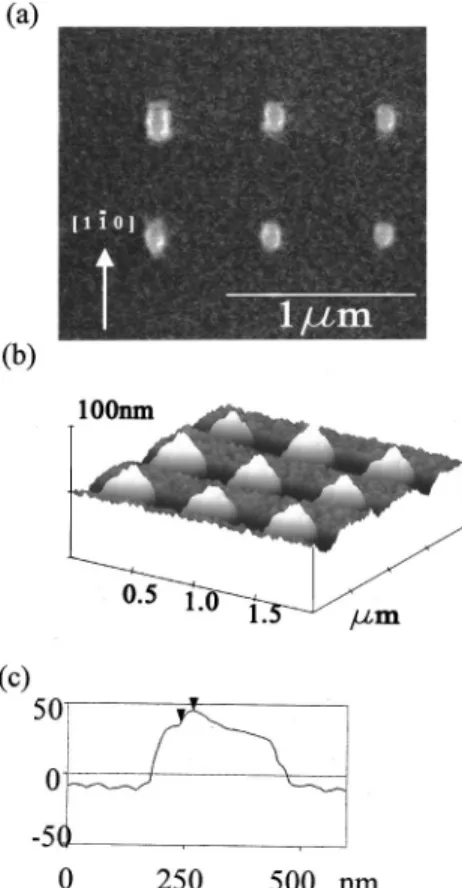
Figure 2共a兲 shows a scanning electron microscopy
共SEM兲 image of the mesa lattice after MBE regrowth. It
shows that the mesas in the lattice are elongated along the
关11¯0兴 direction resulting in a rectangular shape and giving a
new base dimension on the order of ⬃250 nm⫻150 nm. This anisotropic growth is caused by different atom diffusion rates along the two different 具110典 directions. The sample was also studied by a Digital Instruments DI 5000 atomic force microscope 共AFM兲 system using tapping mode. The AFM image is shown in Fig. 2共b兲. It shows that QDs formed on top of the mesas. No dots were found in the nonpatterned region; only surface roughness was observed. Figure 2共c兲 shows a surface profile across a mesa and a single QD. The dots on the mesas have an average base width of ⬃500 Å and an average height of⬃80 Å.
For SK growth mode, the strain is partially relaxed by reorganization of the epilayer material during InAs deposi-tion. Most of the epilayer is rearranged into 3D islands, while the rest remains in a thin wetting layer. With the ap-pearance of 3D islands, the strain distribution changes dras-tically. The transmission electron microscopy 共TEM兲 image in Fig. 3 shows the strain distribution of a single mesa after QD growth. The bright part is the area with little or no strain, which directly proves that no QDs have formed in this non-patterned region. The dark area is where the mesa is located. Because of the added strain layer on the mesa, it appears dark. On top of the mesa, there is an area of strain relief, which appears lighter in the image. But, in the center of the bright spot, there is a small dark region, which is due to the shape of QD. Specifically, because of QD formation, the
strain accumulated is partially relaxed near the periphery of the dot. But because the QD has a pyramid shape, the top appears to be dark. So the change in contrast provides good evidence of single QD formation.
In summary, we have demonstrated a technique for se-lective QD growth. By adding a strain layer in predefined regions, we can control the formation of QDs below the criti-cal thickness at any given region. Single dot formation has been achieved on small e-beam defined mesas. We have also
FIG. 1. Flow diagram of selective growth of single QDs. Sequentially from top to bottom, strain source preparation, e-beam patterning, and MBE
re-growth. FIG. 2. 共a兲 SEM image of a mesa lattice after MBE regrowth, 共b兲 AFM
image of a mesa lattice with QDs on top of the mesa, and共c兲 surface profile across a mesa and a single QD.
FIG. 3. TEM image showing that the strain field on the mesa changes fundamentally due to the formation of single QDs. There is a strain relief area in which there is higher contrast, however, in the center of the dark spot, there is a lower contrast area which is due to the formation of QDs and the partial relaxation of strain.
327
Appl. Phys. Lett., Vol. 80, No. 2, 14 January 2002 Leeet al.
This article is copyrighted as indicated in the article. Reuse of AIP content is subject to the terms at: http://scitation.aip.org/termsconditions. Downloaded to IP: 140.113.38.11 On: Thu, 01 May 2014 06:27:55
achieved two-dimensional arrays of single QDs using this technique. This technique of selectively placing single QDs should find application in many new generation quantum de-vices such as in single electron transistors, distributed feed-back lasers, and single-photon photodetectors.
This work was supported by the National Science Coun-cil under Contract No. NSC 89-2218-E-009-055.
1
N. Kirstaedter, N. N. Ledentsov, M. Grundmann, D. Bimberg, V. M. Us-tinov, S. S. Ruvimov, M. V. Maximov, P. S. Kop’ev, Zh. I. Alferov, U. Richter, P. Werner, U. Go¨sele, and J. Heydenreich, Electron. Lett. 30,
1416共1994兲.
2S. K. Jung, C. K. Hyon, J. H. Park, S. W. Hwang, D. Ahn, M. H. Son, B.
D. Min, Y. Kim, and E. K. Kim, Appl. Phys. Lett. 75, 1167共1999兲.
3
G. Yusa and H. Sakaki, Electron. Lett. 32, 491共1996兲.
4D. S. L. Mui, D. Leonard, L. A. Coldren, and P. M. Petroff, Appl. Phys.
Lett. 66, 1620共1995兲.
5
H. Lee, J. A. Johnson, J. S. Speck, and P. M. Petroff, J. Vac. Sci. Technol. B 18, 2193共2000兲.
6
R. Tsui, R. Zhang, K. Shiralagi, and H. Goronkin, Appl. Phys. Lett. 71,
3254共1997兲.
7
T. Ishikawa, S. Kohmoto, and K. Asakawa, Appl. Phys. Lett. 73,
1712共1998兲.
8S. Kohmoto, H. Nakamura, T. Ishikawa, and K. Asakawa, Appl. Phys.
Lett. 75, 3488共1999兲.
328 Appl. Phys. Lett., Vol. 80, No. 2, 14 January 2002 Leeet al.
This article is copyrighted as indicated in the article. Reuse of AIP content is subject to the terms at: http://scitation.aip.org/termsconditions. Downloaded to IP: 140.113.38.11 On: Thu, 01 May 2014 06:27:55