傳輸線模型下之連線效能最佳化
Performance Optimization Under the Transmission Line Model
計畫編號:NSC 90-2215-E-002-048
執行期限:90 年 8 月 1 日至 91 年 7 月 31 日
主持人:張耀文副教授 臺灣大學電子工程學研究所
一
﹑
中文摘要
隨著操作頻率增加到 Giga Hz 以及訊號上升時間小於 或相等於訊號從導線的一端傳輸到另一端的時間,傳統 利用電阻和電容的 RC 延遲模型(RC delay model)來計算 訊號延遲已經不夠準確。因為在這些情況下計算訊號延 遲需要考慮到傳輸線以及電感的特性。本計畫之目的為 (1)在傳輸線的模型下,發展一個計算時間延遲的解析型 公式;(2)對於一條考慮反射效應的傳輸線,找出其最小 時間延遲的特性;(3)基於我們所提出計算時間延遲的解 析型公式,對導線路徑和繞線樹(routing trees)發展一 個有效的時間延遲最佳化的演算法。 關鍵詞:傳輸線模型,RC 延遲模型,RLC 延遲模型二﹑英文摘要(Abstract)
As the operating frequency increases to Giga Hertz and the rise time of a signal is less than or comparable to the time-of-flight delay of a line, the traditional RC delay model is no longer accurate, and it is necessary to consider the transmission line behavior and the RLC model for delay computation. We propose in this project (1) to develop an analytical formula for the delay computation under the transmission line model, (2) to explore the properties of the minimum delay for a transmission line with the reflection consideration, and (3) to develop effective and efficient optimization scheme for circuit paths and routing trees based on the analytical formula.
Keywords: Transmission line model, RC delay model,
RLC delay model
三﹑
背景和目的
1. Background
As the operating frequency increases to Giga Hertz, the rise time of a signal is less than or comparable to the time-of-flight delay of a line. Also, the die size goes larger. These trends make it important to consider the transmission line behavior for delay computation [1]. When two transmission lines on a chip are connected and these two lines have different characteristic impedance, such mismatches of line impedance can cause reflections from the junction point [1]. Since reflections may cause logic failure or add additional delay, the discontinuities of impedance at junction points must be controlled in order to minimize the side effects of reflections. It is advantageous that a small amount of ringing could help to decrease delay [9]. Therefore, in practice, it is desirable to correctly transmit a signal between the two end points of a transmission line within one round trip, and the first undershoot must be sufficiently small to maintain the signal level.
Transmission phenomenon becomes significant when
t
t
r<
2
.
5
f , wheret
r is the rise time andt
f is thetime of flight determined by the line length l divided by the velocity v [1]. On one hand, if the driver resistance is larger than the line impedance, it requires multiple trips to switch the load; on the other hand, if the driver resistance is smaller than the line impedance, the load may be falsely triggered. We can eliminate the reflections by matching the driver resistance and the line impedance. Because the resistance of a gate or the impedance of a wire is inversely proportional to its width, gate sizing and wire sizing can affect the delay. Thus, sizing circuit components (buffer and wire) can optimize delay under reflection constraints.
Timing is a major concern in the high performance circuits. Many techniques such as wire sizing and gate sizing have been proposed to optimize timing (e.g., [3, 4, 10], etc); however, these techniques are all based on the Elmore delay model [6]. Not much work in the literature considers the minimization of delay under the transmission line model. The algorithm presented in [8] applies continuous wire-sizing to minimize delay under the transmission line model; however, they did not consider the influences of reflections. Besides, there are several previous works that develop modeling and analysis techniques for the simulation and timing characterization under the transmission line model, e.g., [7, 13, 14, 15, 19], but they do not consider delay optimization.
2. Objective
In this project, we focus on the performance optimization and avoid the false switching due to reflections. We shall first develop an analytical formula for the delay computation under the transmission line model and conduct extensive simulations with SPICE to show the accuracy of the formula for transmission lines (both of the lossy and the lossless transmission lines). Based on this formula, we shall explore the properties of a transmission line with reflection considerations. Then, we shall develop an effective and efficient optimization scheme for circuit paths and routing trees based on the analytical formula.
3. Transmission Line Model
When the rise time of a signal is less than or comparable to the time-of-flight delay from one end of a wire to the other end, the wire should be modeled as a transmission line.
3.1. Gate and Wire Modeling
Figure 1 illustrates the gate and the lossy transmission line models used in this project. For a gate i with size
g
i,
the gate resistance
r
bi isr
g
i b
/
ˆ
and the gatecapacitance
c
bi isc
g
i b
ˆ
, wherer
ˆ
b andc
ˆ
b are the unit-sized resistance and unit-sized capacitance of a gate, respectively.A uniform lossy transmission line i of width
w
i can
w
r
w/
i ^ , unit-length inductance,u
w
i w/
^ , and unit-length capacitance,c
ww
i ^ , where ^r
w, ^u
w, andc
ˆ
ware the sheet resistance, the unit-sized inductance, andthe unit-sized capacitance of a wire, respectively. The effect of inductance and capacitance can be represented by a
characteristic impedance,
Z
i , which equals)
(
^^
c
w
u
w i w . The propagation velocity of a wire i,v
i, equals^ ^
1
u
wc
w[1]. If the length of a wire isl
i, its total resistance, total inductance, and total capacitance arer
ˆ
wl
iw
i ,u
ˆ
wl
iw
i , andc
ˆ
ww
il
i , respectively.Figure 1: A gate is the loading of its upstream, but is the driver of its downstream. A lossy transmission line is represented by a serial of its resistance, inductance, and capacitance, or we can merge each section of inductances and capacitances into a characteristic impedance.
Therefore, with the gate and the lossy transmission line models, we can represent a circuit path by resistors, capacitors, and characteristic impedance. Figure 2 illustrates the resulting circuit modeling for a circuit path with n buffers, where
R
S and
C
L are the resistance ofsource and the capacitance of load, respectively.
Figure 2: A circuit path is a combination of resistors, capacitors, and characteristic impedance.
3.2. Reflections on a Wire
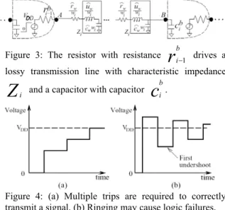
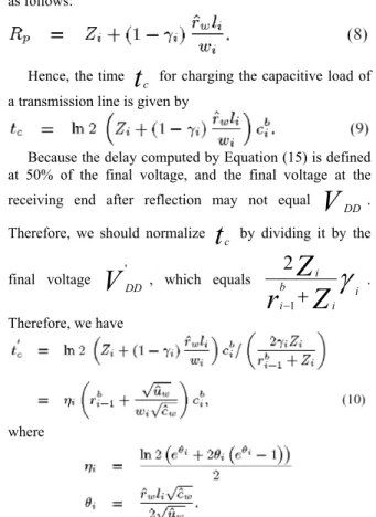
As shown in Figure 3, the gate i-1 drives lossy transmission line i and gate i. Inductive and capacitive discontinuities may occur at the points A and B. Due to the inductive and capacitive discontinuities, the resulting reflections may cause logic failure or excessively longer delay [1]. The initial voltage at the point B is the sum of the signal sent out from the point A and the reflection generated at the point B. When the reflection generated at the point B travels backward to the point A, a new reflection generated at the point A is transmitted toward to the point B. The new voltage at the point B is the sum of the incoming reflection, the new outgoing reflection, and the initial voltage. As shown in Figure 4(a), the initial voltage at point B does not reach the threshold voltage. Thus, multiple round trips along the line may be required to correctly transmit a signal. As shown in Figure 4(b), if the reflection generated at the point A is negative, the voltage may oscillate at the point B, causing overshoot or undershoot. This oscillating pattern is called ringing.
Figure 3: The resistor with resistance
r
bi−1 drives a
lossy transmission line with characteristic impedance
Z
i and a capacitor with capacitorc
b i .Figure 4: (a) Multiple trips are required to correctly transmit a signal. (b) Ringing may cause logic failures.
3.3. Voltage Attenuation on a Wire
On-chip interconnections and some thin film package wires, however, have significant resistance, and they should be treated as lossy transmission lines [5, 16]. When the line resistance becomes larger than the characteristic impedance, resistance dominates the electrical behavior, and the inductive effects disappear. Then the wire should be modeled as a distributed RC line [1, 11].
In a lossy transmission line, the resistance of a line causes voltage attenuation, and the voltage attenuation coefficient
γ
i along a lossy transmission line i is derived
in [1] as follows:
Therefore, in Figure 3, the voltage at the point B before reflection is given by
3.4. When to Use Transmission Line Analysis
According to [1, 11], the transmission line behavior is significant when
and
where
t
r=
2
.
2
r
ib−1(
c
ˆ
ww
il
i+
c
ib)
is the rise time of wire i,t
f=
l
iv
i is the time-of-flight delay,w
l
r
w i iRl
=
ˆ
is the total resistance, andZ
0=
Z
i is the characteristic impedance. As illustrated in Figure 6, we can rewrite Inequalities (3) and (4) as Inequalities (5) and (6) as follows:and
Besides, to make the voltage at the point B correctly
reflections should be greater than or equal to
V
t. In other words, the following inequality must be satisfied.where
Therefore, we should model a line as a lossy transmission line if Inequalities (5)--(7) are satisfied; it should be modeled as a distributed RC line, otherwise.
四
﹑
研究方法
We shall in this form discuss the problem formulation, delay model, Buffer and Wire Sizing for a Circuit Path, and Buffer and Wire Sizing for a Routing Tree.
1. Problem Formulation
In this project, we shall first develop an analytical formula for the delay computation under the aforementioned transmission line model with the reflection consideration and then develop an effective and efficient delay optimization scheme by sizing the components of circuit paths or routing trees based on the analytical formula. We formulate this problem as follows:
Input: A circuit path/routing tree and the lower and upper bounds for buffer and wire sizes.
Objective: Determine the optimal buffer and wire size for each segment in a circuit path/routing tree, so that delay is minimized.
2. Delay Model
The time
t
c for charging the capacitive load (defined
at 50% of the final value) of the lumped network equals
C
R
p L2
ln
, whereR
p is the pullup resistance and
C
L is the total capacitive load [16, 17, 18]. According to[1], the current that a lossless transmission line can supply is limited by its characteristic impedance. As a result, looking from the receiving end, the line behaves like a resistor with a value
Z
0. In a lossy transmission line, not only its characteristic impedance, but also its partial resistance of the line that causes voltage attenuation supplies the current. If the total resistance of a line causes voltage attenuation, the voltage at the receiving end becomes zero. We know that the voltage at the receiving endV
B equalsV
Ai
γ
inFigure 3. This implies that there is only
( )
γ
i
−
1
percentage of the total resistance for the line between nodes A and B,
r
i+1, causing voltage attenuation. Consequently,
the pullup resistance
R
i for the transmission line is equal to the sum of the characteristic impedance of the line, and partial resistance of the wire, which causes voltage attenuation. We have the pullup resistanceR
i for the line
as follows:
Hence, the time
t
c for charging the capacitive load of a transmission line is given byBecause the delay computed by Equation (15) is defined at 50% of the final voltage, and the final voltage at the receiving end after reflection may not equal
V
DD .
Therefore, we should normalize
t
c by dividing it by the final voltage
V
DD ' , which equalsγ
i i b i iZ
r
−1Z
+
2
. Therefore, we have whereBecause transmission line analysis always gives the correct answer irrespective of the rise time of the driver, delay is the sum of the time-of-flight
t
f along the wire,
and the time
t
c '
for charging the capacitive load [1, 16]. Thus, the propagation delay
(
g
g
)
i i−1
,
∆
from the gateg
i 1− to the next gateg
i in Figure 3 is given by
where n is the number of required round trips to correctly transmit a signal.
3. Buffer and Wire Sizing for a Circuit Path 3.1. Reflection Considerations
In practice, designers typically desire to optimize performance without generating undesirable reflections and transmit a signal correctly within a limited number of round trips. As the VLSI technology advances, the wire length is increasing and the capacitance of a gate is decreasing, making the time-of-flight delay dominate the delay. Therefore, we have the following theorem for the optimal number of round trips for delay optimization.
Theorem 1: The minimum delay for a circuit path with
reflection occurs when the number of round trips equals one. Thus, we can rewrite Equation (11) as follows:
3.2. Optimal Wire Sizing
In this section, we minimize the delay of a circuit path by wire sizing. If all buffer sizes and locations are fixed, the delay function of a circuit path from the source s to sink t with n+1 segments (
w
1, …,w
n 1+ ) can be calculated as follows:where
Notice that Equation (13) is a posynomial function in
w
1, …,w
n 1+ , implying that the wire-sizing problemhas a unique global minimum [2]. Thus, we can apply any efficient search algorithm, such as the well-known gradient search procedure, to find a locally optimal solution and thus the globally optimal solution.
3.3. Optimal Buffer Sizing
Similar to wire sizing, assume that all wire sizes and buffer locations are fixed, the delay function of a circuit path from the source s to sink t with n segments (
g
1, …,
g
n) can be calculated as follows:Notice that Equation (14) is also a posynomial function in
g
1, …,
g
n
,
implying that the buffer-sizing problemhas a unique global minimum [2]. Thus, we can apply any efficient search algorithm, such as the well-known gradient search procedure, to find a locally optimal solution and thus the globally optimal solution.
3.4. Optimal Simultaneous Buffer and Wire Sizing
Again, assume that all buffer locations are fixed, the delay function of a circuit path from the source s to sink t with 2n+1 segments (
w
1, …,w
n 1+ ,g
1, …,
g
n) isthe same as Equation (14).
Notice that Equation (14) is also a posynomial function in
w
1, …,w
n 1+ ,g
1, …,g
n , implying that thesimultaneous wire- and buffer-sizing problem has a unique
global minimum [2]. Thus, we can apply any efficient search algorithm, such as the well-known gradient search procedure, to find a locally optimal solution and thus the globally optimal solution.
五﹑
成果 (Publications)
1. S.-R. Pan and Y.-W. Chang, ``Performance optimization by wire/buffer sizing under the transmission line model," in Proceedings of The 11th VLSI Design/CAD Symposium, Pingdong, Taiwan, Aug. 2000
2. T.-C. Chen, S.-R. Pan, and Y.-W. Chang, ``Performance optimization by wire and buffer sizing under the transmission line model," in Proc. of IEEE International Conference on Computer Design (ICCD-01), pp. 192--197, Austin, TX, Nov. 2001.
3. T.-C. Chen, S.-R. Pan, and Y.-W. Chang, ``Performance optimization by wire and buffer sizing under the transmission line model," in revision, IEEE Trans. VLSI Systems.
六
﹑
參考文獻
1. H. B. Bakoglu, Circuit, Interconnections and Packaging for VLSI, Addison-Wesley Publishing Company, Inc., 1990.
2. M. S. Bazaraa, H. D. Sherali, and C. M. Shetty, Nonlinear Programming: Theory and Algorithms, John Wiley and Sons, Inc., NY, 1993.
3. C. P. Chen, Y. P. Chen, and D. F. Wong, ``Optimal Wire-Sizing Formula Under the Elmore Delay Model,'' in Proc. of IEEE/ACM Design Automation Conference, pp. 487--490, June 1996.
4. C. P. Chen, C. C. N. Chu, and D. F. Wong, ``Fast and Exact Simultaneous Gate and Wire Sizing by Lagrangian Relaxation,'' in Proc. of IEEE/ACM Int. Conf. on Computer Aided Design, pp. 617--624, November 1998.
5. A. Deutsch, et al., ``When are Transmission-Line Effects Important for On-Chip Interconnections?,'' in IEEE Trans. on Microwave Theory and Techniques, vol. 45, pp. 1836--1846, Oct 1997.
6. W. C. Elmore, ``The Transient Response of Damped Linear Networks with Particular Regard to Wide Band Amplifiers,'' in J. Applied Physics, Vol. 19, No. 1, 1948.
7. K. Gala, V. Zolotov, R. Panda, B. Young, W, Junfeng, D. Blaauw, ``On-Chip Inductance Modeling and Analysis,'' in Proc. of IEEE/ACM Design Automation Conference, pp. 63--68, 2000.
8. Y. Gao and D. F. Wong ``Shaping a VLSI Wire to Minimize Delay Using Transmission Line Model,'' in Proc. of IEEE/ACM Int. Conf. on Computer Aided Design, pp. 611--616, November 1998.
9. Y. Gao and D. F. Wong ``Wire-sizing for Delay Minimization and Ringing Control Using Transmission Line Model,'' in Proc. EDAC, pp. 512--516, 2000.
10. H. R. Jiang, J. Y. Jou, and Y. W. Chang, ``Noise-Constrained Performance Optimization by Simultaneous Gate and Wire Sizing Based on Lagrangian Relaxation,'' in Proc. of IEEE/ACM Design Automation Conference, pp. 90--95, June 1999.
11. F. Moll, M, Roca, A. Rubio, "Inductance in VLSI interconnection modeling," Circuits, Devices and Systems, IEE Proceedings, vol. 145, issue 3, pp. 175--179, June 1998.
12. S. G. Nash and A. Sofer, Linear and Nonlinear Programming, McGraw-Hill, Inc., 1996.
13. R. Gupta, S. Y. Kim, L. Pilegggi, ``Domain Characterization of Transmission Line Models and Analyses,'' in IEEE Trans. Computer-Aided Design of Integrated Circuits and Systems, vol. 15, NO. 2, pp. 184--193, Feb 1996.
14. R. Gupta, L. Pilegggi, ``Modeling Lossy Transmission Lines Using the Method of Characteristics,'' in IEEE Trans. on Circuits and Systems I, vol. 43, NO. 7, pp. 580--582, Jul 1996.
15. R. Gupta, B. Krauter, L. Pilegggi, ``Transmission Line Synthesis via Constrained Multivariable Optimization,'' in IEEE Trans. on Computer-Aided Design of Integrated Circuits and Systems, vol. 16, NO. 1, pp. 6--19, Jan 1999.
16. Jan M. Rabaey, Digital Integrated Circuits: A Design Perspective, Prentice Hall, Inc., 1996.
17. J. Rebinstein, P. Penfield, Jr., and M. A. Horowitz, ``Signal Delay in RC Tree Networks,'' in IEEE Trans. on CAD, vol. CAD, pp. 202--211, Jul 1983.
18. W. Wolf, Modern VLSI Design: Systems on Silicon, 2nd Editon Prentice Hall, Inc., 1996.
19. Q. Yu and E. S. Kuh, ``Exact Moment Matching Model of Transmission Lines and Application to Interconnect Delay Estimation,'' in IEEE Trans. VLSI Systems, vol. 3, no. 2, pp. 311--322, June 1995.