1
Don’t-Care Bits Filling for Capture Power
Reduction
Lung-Jen Lee1, Wang-Dauh Tseng, Rung-Bin Lin, and Zheng-Yi Xie
Department of Computer Science & Engineering Yuan Ze University, Chung-li, Taiwan, 32026, ROC
1s959101@mail.yzu.edu.tw
Abstract-In this paper, we propose a don’t-care-bit filling method to successfully reduce the test power dissipation during capture cycles. An induced activity function is applied on each scan cell which estimates the potential on incurring cascaded transitions in the circuit under test (CUT) and obtain an optimal order for don’t care bit filling. Results show, this method reduces switching activity in the CUT up to 40% during the capture cycles compared with random X-filling method, and outperforms LCP X-filling method. Moreover, no area and performance overhead are incurred.
Index Terms-X-filling, capture power, LCP X-filling
1.INTRODUCTION
Power consumption during test application is significantly higher than that during the circuit’s normal operation. It was reported in [1] that the power consumed during test could be twice as high as the power consumed during normal operation. Excessive power consumption may cause logical error in a fault-free chip leading to an unnecessary loss of yield and may even destroy chip during test [2]. Hence, it is important to limit the power consumption during test application.
In the capture cycle, the test vector loaded in the scan chain during the shift cycle is applied to the combinational part of the circuit and the response of the circuit is captured into the scan chain. For a scan cell, if the bit value in the applied test vector differs from that in the captured response, a transition will occur. For ease of description, throughout this paper, we refer to such two bits on a scan cell as “bit-pair”. The transition in the flip-flop will induce other gates in combinational
part of the circuit to switch. High density of switching activity occur in both the scan chain and the circuit under test (CUT) during a capture cycle can lead to excessive power consumption which may produce a high voltage drop which can corrupt the test response of the circuit. Therefore, reducing power consumption during capture cycle is critical for avoiding manufacturing yield loss [3]. However, compared with reducing test power during shift cycles, test power reduction during capture cycle is a less researched area. Only few techniques have been proposed to reduce the power during capture cycle [3]-[5]. The idea of [5] is assigning 0’s or 1’s to don’t-care bits in test vectors to reduce the switching activity in capture cycles. The order of don’t-care bits in response to be assigned is determined basing on the number of available don’t -care bits at primary inputs. Certain don’t-care bits are ensured to be with higher probability of successful justification. However, transitions at some scan cells causing a lot of switch activities in the circuit may fail to be reduced under the above priority strategy. In a fully specified test set, the method in [6] is designed for identifying as many don’t-care inputs of test vectors as possible. It applies the line justification operation similar to D algorithm to select the fault propagation paths. Those values of test vector on the inputs which are reachable by the fault propagation paths will be preserved while those not reachable will be marked as don’t-cares. This technique manipulates more don’t-care bits, thus more transitions will be reduced.
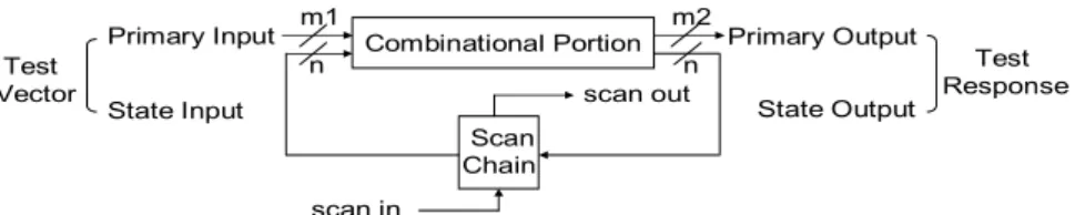
2 Combinational Portion Primary Input m1 Scan Chain scan in scan out n State Input m2 Primary Output State Output n Test Vector Test Response
Figure 1. A general full-scan circuit
In this paper, we combine the idea in [5] and utilize an induced activity function [7] to reduce power dissipation in capture cycles. Depending on the circuit structure, the transitions at some inputs cause more transitions at internal nodes than those at other inputs. The induced activity function can help give priority to each scan cell by which a don’t-care bit assigning order is scheduled. This order can effectively solve the conflicting problem during justifications and promise to minimize total induced transitions in a capture cycle.
Section 2 introduces the proposed don’t-care- bit-filling method. An experiment is carried out on ISCAS’89 benchmark circuits in section 3. Section 4 concludes the paper.
2. PROPOSED METHOD
Generally, a full-scan sequential circuit, as shown in Figure 1, is composed of a combinational part with m1 primary inputs and m2 primary outputs as well as n scan flip-flops which are connected serially as a chain. During testing, the n state inputs are applied from scan chain and then state outputs captured replacing current scan chain contents. The state input bit and state output bit occurred on the same flip-flop in some capture cycle thus form a “bit-pair” which is mentioned throughout this paper.
For scan-based circuit architecture, every scan cell impact the CUT differently due to their different cones spanned in the circuit structure. A transition on a scan cell during capturing During each capturing, the transitions in the CUT induced by the transition occurred on each scan cell are quite different. To efficiently reduce the induced transitions in a capture cycle, minimizing total transitions in the scan chain by properly assigning
don’t-cares in the bit-pair for each scan cell is a viable solution. However, some don’t cares may exist in state outputs, in order to fill the don’t-care bit in state output with proper value, we apply line justification algorithm [8] from the state output bit to related primary inputs. All nodes on the paths will be justified according to the desired logic value in state output. Finally, one more bit-pair is set to be (1, 1) or (0, 0) and one less transition will occur on the scan cell during capture cycle. Note that, during justification, the back tracking branches in the CUT justified from different state output bits may overlap each other. This implies conflicts may occur if results of justifications tracked back to same input ends but different logic values. In [7], the authors propose a gain function, called induced activity function, to identify among the inputs of the circuit that cause more transitions at internal nodes. This function measures the impact of a transition at a specified input on the switching activity of the complete circuit depending on its fanout value and is calculated from both the transition density Dpi(x) on each node x in the circuit and the fanout Fan(x) of the nodes. For each input pi, this function Fpi is briefly given by:
∑
∀ = x Fan(x) Dpi(x) Fpi (1)In order to measure the impact on the complete circuit caused by the transition on each position of scan chain, we modify this gain function and apply it on each scan cell. This doing provides us important information about the impact of each scan cell on the circuit. A scan cell with higher weight implies that the transition on it induces more other switching activity in CUT during capturing. By this information, we order the
3
Table I. Four cases of bit values in state input and state output
Case type Bit in state input Bit in state outputBit-pair
Case 1 0 or 1 0 or 1
Case 2 X 0 or 1
Case 3 0 or 1 X
Case4 X X
assigning process for those bit-pairs with don’t-care bits and thus, solve the conflict problem.
Table I describes four cases of bit values in the pair of state input and state output.
For case 1, both bits in bit-pair are already specified, so no action is taken.
For case 2, only the state input bit is don’t-care bit. We can reduce transitions occurred in capture cycles by simply filling don’t-care bits to make the bit-pairs (1, 1) or (0, 0) according to the logic value of target state output bit in a bit-pair.
For case 3, only the state output bit is don’t-care in the bit-pair. Line justification algorithm is applied on state output bit by setting it to the same logic value as current state input in the same bit-pair. A successful justification assigns one don’t-care bit in primary input to 1 or 0 and ensures the equivalence in the bit-pair.
However, due to the intrinsic limitation of circuit architecture, conflicts may occur among line justifications on two state outputs. The proposed method performs induced activity function on each scan cell and give priority to each bit-pair during don’t cares assigning.
For case 4, both bits in bit-pair are don’t-care. Two steps are taken. The first step is to assign 1 or 0 to the state input bit. It’s similar to case 2, except that it makes a decision for choosing 1 or 0 first to perform the assignment because state output bit is also don’t-care bit in case 4. In the proposed method, this decision is made in such way that it fulfils MT-fill [9] as the first choice. The second step is to justify the same value on state output, same as case 3. If this is successful, the probable transition on this scan cell during capture cycle will be eliminated. If not successful, return to the first step with taking the other assignment (0 or 1) on state input and then go through the line justification
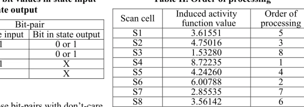
Table II. Order of processing
Scan cell Induced activity function value processingOrder of
S1 3.61551 5 S2 4.75016 3 S3 1.53280 8 S4 8.72235 1 S5 4.24260 4 S6 6.00788 2 S7 2.85535 7 S8 3.56142 6
on state output. If it is still not successful, the proposed method complies with MT-fill to assign don’t-care bit in state input to reduce the transitions during shift cycles.
The overall algorithm of our proposed method is illustrated as follows. First, for each circuit, it calculates the induced activity function value for every scan cell to decide the order of corresponding bit-pairs during execution. Second, for each test, it performs assignment, justification, both of them, or MT-fill assignment on those bit-pairs in the sequence determined in previous step. It is done until no more don’t-care bit in the test vector or response can be filled following the case procedure. The overall process is done until all test set have been manipulated.
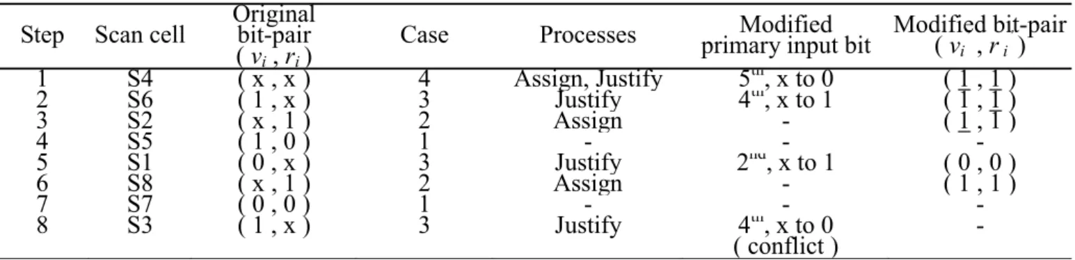
The following is an example. Consider a CUT with six primary input bits, four primary output bits, and one scan chain composed of eight scan cells. Table II shows the induced activity function values on each scan cell and the order in which bit-pairs corresponded to each cell are manipulated in the second step of proposed method. The bit-pairs on cell with larger values of induced activity function would be processed prior to others because the transitions on these bit-pairs during capture cycle will cause more switching activities then others. In this example, the order among eight scan cells is S4, S6, S2, S5, S1, S8, and S7. For the second step in algorithm, consider one test vector: 1x0xx1 0x1x110x as v and its test response: 001x x1xx0x01 as r. Figure 2 shows the relation between v and r in the CUT during capture cycle. For each bit-pair ( vi , ri ), Table III lists the categorization of
cases, the processes took on it according to the case, and the modified primary input bit and bit-pair
4 1 X 0 X X 1 Primary Input 0 0 1 X Primary Output State Input State Output Combinational Portion 1 X 1 1 0 X X 0 X X 0 X 0 1 1 X
Scan in Scan out
Figure 2. Relation between test vector and test response in CUT Table III. Illustration of procedures
Step Scan cell Original bit-pair ( vi, ri )
Case Processes Modified primary input bit Modified bit-pair( v
i’ , r i’ ) 1 S4 ( x , x ) 4 Assign, Justify 5th, x to 0 ( 1 , 1 ) 2 S6 ( 1 , x ) 3 Justify 4th, x to 1 ( 1 , 1 ) 3 S2 ( x , 1 ) 2 Assign - ( 1 , 1 ) 4 S5 ( 1 , 0 ) 1 - - -5 S1 ( 0 , x ) 3 Justify 2nd, x to 1 ( 0 , 0 ) 6 S8 ( x , 1 ) 2 Assign - ( 1 , 1 ) 7 S7 ( 0 , 0 ) 1 - - -8 S3 ( 1 , x ) 3 Justify 4th, x to 0 ( conflict )
-( vi’ , r i’ ). Table IV shows the evolvement of test
vector v and test response r. Note that there is nothing done for modification in step 4, 7, and 8. Among them, conflict situation is occurred in step 8. Therefore, no further modification has performed. In step 4 and 7, they are both case 1 and no action is supposed to be performed.
3. EXPERIMENTAL RESULTS
To validate the reduction of power dissipation during capture cycles by the proposed method, ten ISCAS’89 benchmark circuits are applied for experiments. The test set generations are implemented by SynTest Turbo Scan which generates a test set with don’t-care bits for all circuits. The generated test set is without random fill and static compaction. The total algorithm including proposed method and calculations of induced activity function at every scan cell is programmed in C language. The Power
Table IV. Evolvement of primary input, state input and state output
Step Primary
input State input State output 0 1 X 0 X X 1 0 X 1 X 1 1 0 X X 1 X X 0 X 0 1 1 1 X 0 X 0 1 0 X 1 1 1 1 0 X X 1 X 1 0 X 0 1 2 1 X 0 1 0 1 0 X 1 1 1 1 0 X X 1 X 1 0 1 0 1 3 1 X 0 1 0 1 0 1 1 1 1 1 0 X X 1 X 1 0 1 0 1 4 1 X 0 1 0 1 0 1 1 1 1 1 0 X X 1 X 1 0 1 0 1 5 1 1 0 1 0 1 0 1 1 1 1 1 0 X 0 1 X 1 0 1 0 1 6 1 1 0 1 0 1 0 1 1 1 1 1 0 1 0 1 X 1 0 1 0 1 7 1 1 0 1 0 1 0 1 1 1 1 1 0 1 0 1 X 1 0 1 0 1 8 1 1 0 1 0 1 0 1 1 1 1 1 0 1 0 1 X 1 0 1 0 1
consumption on each circuit is estimated by counting the number of transition counts during capture cycles. In order to realize the effectiveness of our proposed method, we also implement LCP X-filling in [5] by C language as a comparison. The results of the experiments are also compared with random X-filling method.
Only the transitions in capture mode are concerned in this experimental design because this
5
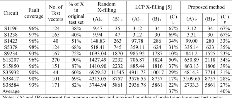
Table V. Comparison of proposed method and LCP X-filling to random X-filling
Circuit coverage Fault
No. of Test vectors % of X in original test set Random
X-filling LCP X-filling [5] Proposed method (A)R (B) R (A) L (B) L (C) L (A) P (B) P (CP )
S1196 96% 124 38% 9.47 35 3.12 34 67% 3.12 34 67% S1238 97% 165 40% 9.94 47 3.12 30 69% 3.31 30 67% S1423 96% 40 51% 148.83 263 97.78 286 34% 99.00 280 33% S5378 98% 124 68% 518.41 745 359.11 624 31% 335.14 623 35% S9234 93% 167 72% 1093.04 1870 985.92 1787 10% 841.2 1525 23% S13207 96% 270 90% 1427.49 2232 706.87 1824 50% 650.89 2118 54% S15850 96% 151 87% 1410.90 2232 885.44 1816 37% 863.13 1806 39% S35932 90% 44 60% 6929.52 11545 4911.73 10017 29% 4814.3 7714 31% S38417 98% 101 69% 4313.05 8757 3576.55 8757 17% 3109.65 8757 28% S38584 93% 171 82% 3744.94 5861 2936.78 5861 22% 2733.3 5861 27% Average 37% 40%
Notes: (A) and (B) represent the average number and maximal number of node transitions per test vector. (C) is the reduction percentage of total node transitions and is calculated as (C) L= [ (A)R - (A) L] / (A)R *100% and (C) P= [ (A)R - (A) P] / (A)R *100%.
research is focused on the reduction of power consumption generated during captures cycles. In capture mode, the average number of node transitions per test vector and the maximum number of node transitions among all test vectors are shown in Table V for each method. The fault coverage, the number of test vectors, and the percentage of don’t-care bits in the original test set are also reported. The reduction percentages of total node transitions in capture cycles compared to
random X-filling method are obtained for both LCP X-filling and our approach.
The result shows that our proposed method achieved about 40% reduction on average node transitions and 14% reduction on maximal node transitions in capture mode in average of ten circuits as compared with random X-filling method. In most cases, we can get higher reduction rate on both average and maximal node transitions than the LCP X-filling [5].
4. CONCLUSIONS
In this paper, to avoid the yield loss due to faulty response capturing in a fault free circuit, we propose a don’t-care-bit filling method to reduce the test power dissipation during capture cycles. Combing an induced activity function, the optimal order in assigning the don’t-care bits in test vectors or responses is obtained so as to prevent larger potential switching activity in CUT during capture cycles. This method assigns proper 0’s or 1’s to don’t-care bits on test vectors or response without any area overhead. Induced activity function can help deal with the conflict problem while double
assignments occurred on the same don’t-care bit in primary inputs. Experimental results show 40% reduction on excessive power consumption in capture mode as compared with random X-filling method and, in most cases, higher reduction rate than the LCP X-filling [5].
REFERENCES
[1] Y. Zorian, “A distributed BIST control scheme for complex VLSI devices,” in Proc. 11th
IEEE VLSI Test Symp., Apr. 1993, pp. 4-9.
[2] N. K. Jha and S. Gupta, Testing of Digital
Systems, Cambridge University Press, 2003.
6 Nicolici, “Scan architecture for shift and capture cycle power reduction,” in Proc.
International Symposium on Defect and Fault Tolerance in VLSI System, 2002, pp. 129-137.
[4] K.-J. Lee, S.-J. Hsu and C.-M. Ho, “Test power reduction with multiple capture orders,” in
Asian Test Symposium, Nov. 2004, pp. 26-31.
[5] X. Wen, Y. Yamashita, S. Kajihara, L.-T. Wang, K. K. Saluja, and K. Kinoshita, “On low-capture-power test generation for scan testing,” in VLSI Test Symposium, May 2005, pp. 265-270.
[6] K. Miyase and S. Kajihara, “XID: Don't-care identification of test patterns for combinational
circuits,” IEEE Trans. Computer-Aided Design, Vol. 23, No. 2, pp. 321-326, Feb. 2004.
[7] P. Girard, L. Guiller, C. Landrault, and S. Pravossoudovitch, “A test vector ordering technique for switching activity reduction during test operation”, in Proc. 9th Great Lakes Symp. VLSI, Mar. 1999, pp.24-27.
[8] M. Abramovici and M. A. Breuer, Digital
Systems testing and testable design, IEEE
Press, 1990.
[9] R. Sankaralingam and N. A. Touba, "Controlling peak power during scan testing," in Proc. VLSI Test Symposium, 2002. pp153 - 159.