行政院國家科學委員會專題研究計畫 成果報告
矽鍺量子點奈米級記憶元件及陣列之製作與研究(3/3)
研究成果報告(完整版)
計 畫 類 別 : 個別型 計 畫 編 號 : NSC 95-2221-E-002-366- 執 行 期 間 : 95 年 08 月 01 日至 96 年 07 月 31 日 執 行 單 位 : 國立臺灣大學電子工程學研究所 計 畫 主 持 人 : 管傑雄 共 同 主 持 人 : 蔡振水 計畫參與人員: 博士班研究生-兼任助理:蔣光浩 碩士班研究生-兼任助理:沈冠源、呂紹維 處 理 方 式 : 本計畫可公開查詢中 華 民 國 96 年 12 月 10 日
行政院國家科學委員會補助專題研究計畫成果報告
矽鍺量子點奈米級記憶元件及陣列之製作與研究
計畫類別:■個別型計畫 □整合型計畫
計畫編號:NSC 95-2221-E-002-366-
執行期間:
93 年 8 月 1 日至 96 年 7 月 31 日
計畫主持人:管傑雄
共同主持人:蔡振水
計畫參與人員:蔣光浩、呂紹維、沈冠源
執行單位:
國立台灣大學電子工程研究所中 華 民 國
96 年 9 月 29 日
矽鍺量子點奈米級記憶元件及陣列之製作與研究
計畫編號:NSC 95-2221-E-002-366-
執行期間:93 年 8 月 1 日 至 96 年 7 月 31 日
主持人:管傑雄 台灣大學電子工程系教授
一、中文摘要 傳統快閃記憶體存在尺寸微縮的限制, 即現今元件面臨最重要的問題之ㄧ。絕緣層厚 度影響了元件微縮的問題,特別是穿透氧化層 (tunnel oxide) 的厚度。當穿透氧化層厚度不斷 下降,卻與快閃元件所需要的最小厚度以達到 元件的可靠度相違背。換句話說,在保存模式 下 (retention),穿透氧化層需要提供較佳的絕 緣性進而維持超過十年以上的資料。然而,快 閃記憶體為了達到十年以上保存特性需要設 計較厚的穿透氧化層的厚度,相對來說這卻與 寫入與抹除的速度相矛盾 在穿透氧化層中的一個缺陷足夠創造一 個漏電的路徑,使得在浮動閘極裡電荷流失 掉,進而影響元件長期的非揮發性。使用奈米 晶體 (nanocrystals, NCs) 當作非揮發性記憶 體元件的浮動閘極在文獻中引起廣泛的研究 主要因為其優秀的電性和較高的微縮能力。與 傳統非揮發性記憶體比較,在奈米晶體非揮發 性記憶體中,電荷不是儲存在連續多晶矽浮動 閘極,而儲存在一層互相獨立,隔絕的結晶化 的奈米晶體或奈米點來降低傳統快閃記憶體 所遭遇電荷流失的問題,進而可以允許較薄穿 透氧化層且不會犧牲非揮發性,因此元件可以 操作在更小的操作電壓,較佳的耐用性和較快 的寫入與抹除速度,因為所儲存的電荷與氧化 層的缺陷較不敏感而且奈米點之間的間距可 以抑制從橫向路徑所造成的電荷流失。 在我們的研究中,我們使用鍺奈米晶體 (Ge nanocrystals)在二氧化矽(SiO2)中作為浮動 閘,製作出三層結構的金氧半電容元件。首 先,我們使用化學氣相沉積在二氧化矽上形成 鍺奈米晶體。在超高真空化學氣相沉積系統中, 一開始使用甲烷在二氧化矽表面上沉積隨機分布的矽原子核(Si nuclei)。接著,再通入 GeH4
氣體,並選擇在矽原子核上成長。而我們也另 一種物理氣相沉積的方法來製作鍺奈米晶體 埋在二氧化矽中。鍺奈米晶體是利用電子槍蒸 鍍機在二氧化矽上形成一層非晶鍺薄膜後再 經過高溫爐的退火來達成。從SEM 及 HRTEM 下,我們確實觀察到結晶化的鍺奈米晶體埋在 二氧化矽中。對於利用化學汽相沉積所形成的 鍺奈米晶體,在經過高溫熱退火 (PDA) 後, 其電荷保存的特性有明顯的改善。而利用蒸鍍 法所形成的鍺奈米晶體,我們發現在乾氧中所 形成之鍺奈米晶體有較好的電荷保存的特性。 對於電荷流失的機制,我們建立了一個陷 阱模型來證實電荷保存的特性與電荷流失的 時間常數的關係。我們的模型是建立在 SRH 的理論上在加入一個電荷流失的時間常數。我
們首先量測電容與電導對電壓的關係。再把陷
阱 電 容 (Trap capacitance) 跟 電 導 (Trap
conductance) 求出進而求出電荷流失的時間 常數 (charge loss time constant)。我們比較其 利用蒸鍍法所形成的鍺奈米晶體電容元件在
經過PMA 前後其電荷流失時間常數的改變。
本研究認為較小的電荷流失時間常數屬於較 淺的缺陷 (shallow trap) 部分。在經過 PMA 後的元件擁有較大的時間常數,其元件中較淺 的缺陷大部分被修復。從電保存的特性來看, 以電荷流失常數來分析,其經過PMA 的樣品 並無法從明顯的改善很多,吾人認為從我的量 測 只 能 得 到 的 較 短 電 荷 流 失 常 數 也 就 是 shallow trap 的部份,若要得到較大的時間 常數必須操作在較低頻的實驗上來量測。 英文摘要
Conventional Flash memories have the
scaling limitations. The most prominent one today is the limited potential for continued scaling of the device structure. This scaling limitation from the isolation layers thickness, in particular the tunnel oxide layer. The aggressive scaling of gate dielectric is incompatible with the need to preserve minimum dielectric thickness in flash devices to maintain oxide reliability. On the other hand, the tunnel oxide needs to provide superior isolation under retention in order to maintain the data information over periods of up ten years. However, flash memory cells designed for ten years data retention requiring the use of thick tunnel oxide that compromise both its write and erase speed. One weak spot in the tunnel oxide is sufficient to create a fatal discharge path, compromising long-term nonvolatility. Nonvolatile memory devices using nanocrystals (NCs) as a floating gate (FG) have received considerable attention because of its excellent memory performance and high scalability. As compared to conventionally stacked-gate NVM
devices, in a nanocrystal NVM device charge is not stored on a continuous FG poly-Si layer, but instead on a layer of discrete, mutually isolated, crystalline nanocrystals or‘dots’to reduce the problems of charge loss encountered in conventional flash memories, allowing for thinner injection tunneling oxides without sacrificing nonvolatility and, hence, smaller operating voltages, better endurance, and faster write/erase speeds because stored charges can be less sensitive to local oxide defects and the spacing between the dots suppresses the charge loss through lateral path.
In this work, we use germanium nano-crystals (Ge NCs) as a floating gate in silicon dioxide (SiO2) matrix, and then form a
MOS capacitor with a tri-layer structure. At First, we present a study on the CVD growth of Ge NCs on SiO2. The Ge NCs are grown by a two-step process. First, Si nuclei are deposited on SiO2 surface. Then, Ge is selectively grown on the Si nuclei. We also use a PVD method to synthesize Ge NCs embedded in SiO2 matrix. The Ge NCs are formed by furnace annealing of an E-gun evaporated ultra-thin Ge layer at 900oC for 300 s in a dry N2 ambient. From SEM and
HRTEM measurements, we ensure that Ge NCs exactly are embedded in SiO2 matrix and the
lattice fringes are pronounced. For Ge NCs grown by UHV/CVD system, the charge retention characteristics of the devices followed by PDA treatment is improved. For Ge NCs formed by furnace annealing of E-gun evaporated Ge layer, the better retention characteristic is improved by furnace annealing in a dry O2 ambient.
We also propose a single trap model based on SRH theory by introducing another charge
loss time constant in this model. In our work, we utilize our trap model to compare the charge retention characteristics between the devices with/without PMA treatment. We suggest the defects or surface states around Ge NCs are annealed out with PMA treatment, resulting in smaller amount of communication of charges between NCs/traps and caused by the reduction of conductive paths. The recover of these defects are belong to the shallow traps. During PMA treatment, the shallow traps in the oxide are annealed out, resulting in reduction of trap capacitance and trap conductance but the charge retention is not obviously improved due to the charges storing in the deeper traps or deeper potential well.
二、計畫的緣由與目的
Conventional Flash memories have the scaling limitations. The most prominent one today is the limited potential for continued scaling of the device structure. This scaling limitation from the isolation layers thickness, in particular the tunnel oxide layer. The aggressive scaling of gate dielectric is incompatible with the need to preserve minimum dielectric thickness in flash devices to maintain oxide reliability. On the other hand, the tunnel oxide needs to provide superior isolation under retention in order to maintain the data information over periods of up ten years. However, flash memory cells designed for ten years data retention requiring the use of thick tunnel oxide that compromise both its write and erase speed. Nonvolatile memory devices using nanocrystals (NCs) as a floating gate (FG) have received considerable attention because of its excellent memory performance and high scalability. As compared to conventionally
stacked-gate NVM devices, in a nanocrystal NVM device charge is not stored on a continuous FG poly-Si layer, but instead on a layer of discrete, mutually isolated, crystalline nanocrystals or`dots'to reduce the problems of charge loss encountered in conventional flash memories, allowing for thinner injection tunneling oxides without sacrificing nonvolatility and, hence, smaller operating voltages, better endurance, and faster write/erase speeds because stored charges can be less sensitive to local oxide defects and the spacing between the dots suppresses the charge loss through lateral path.
Compared to Si, Ge has a narrower band gap to provide superior retention time, and has high thermal condensation ability during high temperature process. Otherwise, the formation of Ge nanocrystals is compatible to the typical CMOS process. Y.-C. King et al. proposed a technique of Ge NCs formation in gate dielectric of a MOSFET through a sequence of thermal oxidation of Si1-xGex at various temperature
followed by high-temperature annealing [1]. Besides, the Ge NCs are usually formed by various other methods, such as a rapid thermal annealing (RTA) of co-sputtering Ge +SiO2 layer
[2], Ge implantation into SiO2 films [3], H2
reduction of Si1-xGexO2 or Ge-oxide [4],
ultra-thin electron-beam evaporated Ge layer embedded in SiO2 [5]. Thus co-sputtering allows
one to vary the Ge content in a vary broad range. Ion implantation allows incorporating more Ge species into the SiO2,but makes some damage in
SiO2 matrix. For previous fabrication methods, it
is difficult to control the thickness of the tunneling and control oxide layer, as well as the density and size of the Ge NCs. Recently, Ge
NCs or SiGe dots on SiO2 or a high–k dielectric
have been performed by chemical vapor deposition [6][7]. Figure 1-1-4 shows the schematic of various fabrication methods of Ge nanocrystals embedded in the SiO2 matrix in the
literatures.
In our work, the key process is the formation of Ge nanocrystals embedded in SiO2
matrix. The difficulty of the NCs formation is the size control and density. We use the two methods include chemical vapor deposition and physical vapor deposition to form Ge NCs. For CVD methods, we use a two-step process with ultrahigh vacuum chemical vapor deposition system. In addition, we use electron-gun thermal evaporator to evaporate ultrathin amorphous Ge film on thermal oxide and then cap with SiO2
film on Ge film to form tri-layer structure followed by thermal annealing treatment. Then, we form the MOS capacitor to be nonvolatile memory structure. The electrical performance of charge storage and retention characteristics will
be discussed. Finally, we analyze the
experimental results using a trap model to study the charge exchange from communication between Ge NCs and Si substrate and charge loss mechanism in the evaporated Ge NCs based nonvolatile memory capacitor for comparison between the devices with/without PMA treatment.
In the past literatures, the formation of Ge nanocrystals is extensively investigated in different methods consist of Ge ion implantation into SiO2 matrix, oxidation of poly SixGe1-x film
on Si substrate or thin SiO2 layer, and
co-sputtering of Ge + SiO2 followed by thermal
treatment, etc. For previous fabrication methods, it is difficult to control the thickness of the
tunneling and control oxide layer, as well as the density and size of the Ge NCs. In our work, we propose a two step process using a commercial ultra-high vacuum / chemical vapor deposition (UHV/CVD) system. This two-step process has been proposed using LPCVD (low temperature chemical vapor deposition) by T. Baron et al. in
2003 [8]. The UHV/CVD system was
demonstrated by Meyerson in 1986 [9]. The system consists of a growth chamber, a loading chamber, and a computer-control gas source switching box. The reaction chamber utilizes a hot-wall isothermal furnace with a quartz tube of 6 inches in diameter. The furnace is a conventional 3-zone furnace with a flat temperature zone. The bass pressure in the growth chamber is about 2 ×10⁻⁸ Torr.
On the other hand,compared to the various methods of Ge NCs formation in the literatures, another physical vapor deposition (PVD) method, i.e. electron-gun (E-gun) thermal evaporator system to form Ge NCs is also used in our work differently from the chemical vapor deposition (CVD), i.e. UHV/CVD. This high vacuum e-gun evaporation system consists of an e-beam gun with a four-crucible hearth. It can evaporate four different materials without breaking the vacuum. A crystal monitor will monitor the film deposition ratio and thickness. The vacuum system is configured with a roughing pump and a cryopump. The typical base pressure is 2x10⁻⁷ Torr. E-beam evaporator can deposit refractory metals such as W, Ta and Mo. Inside the high vacuum chamber a high-energy e-beam is focused onto the surface of source materials. The kinetic energy of electrons is transformed to heat via the impact. The overall energy released can be as high as several million watts per square
inch. Therefore the heat can melt any refractory materials. The hearth which holds the evaporate materials is water-cooled to keep from overheating and melting.
In our work, one of the advantages that we use E-gun evaporator to form Ge NCs is not expensive compared to UHV/CVD system and easily try different size of Ge NCs from various thicknesses of the evaporated amorphous Ge films. The fabrication process of Ge NCs using the E-gun system is as follows: Firstly, a rapid thermal oxide (RTO) layer with a thickness of 3 nm is grown on a p-type Si substrate followed by RCA clean. Next, the sample and the crucible with pure Ge granules (99.999%) are loaded in the chamber in the E-gun evaporator system. When the pressure of the chamber is lower than 1E-4 Pa, the vacuum for evaporation is ready. Because the melting point of Ge is around ~938oC, we increase the current to make the Ge granules melting. Then, an amorphous Ge (a-Ge) layer is deposited on the RTO layer by E-gun evaporation. Ge is evaporated at a rate of about 0.1 Åsec-1. The z-ratio of Ge is 0.516 and the density is 5.4 g/cm3. After the a-Ge layer deposition, we evaporate titanium (Ti) ~1000 Å to coverage the a-Ge near the crucible in order to prevent the Ge evaporating to contaminate the non-Si based sample in the next evaporation due to the thermal radiation. Finally, a SiO2 layer
(~40 nm) is capped on the a-Ge layer by the PECVD system as the control oxide. The three-layer structure (tunnel SiO2/RTO/ a-Ge
layer/Capping SiO2) is then heated by furnace
annealing treatment in a dry N2 ambient at 900oC
for 300 seconds. This thermal treatment is called “PDA.” The PDA treatment is in order to form well-separated Ge NCs.
三、研究方法及成果
In our work for Ge NCs fabrication using the UHV/CVD system and E-gun evaporator, we observer these device structure characteristics under various growth conditions, such as the growth temperature and durations for UHV/CVD system and the thickness of the evaporated a-Ge films followed by PDA treatment for E-gun evaporation. These results about the dot size and density obtained from the SEM and HRTEM images.
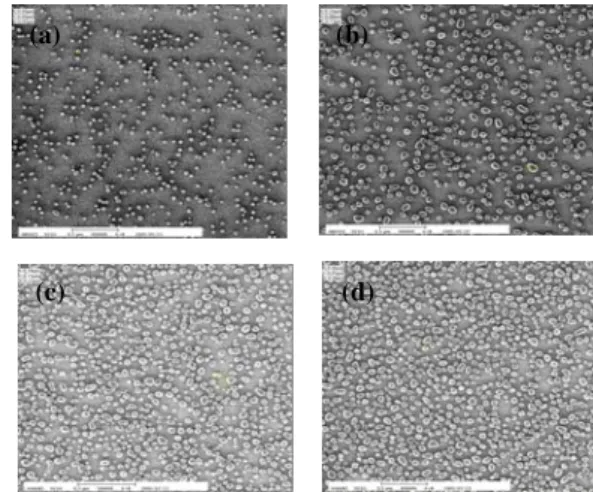
It is shown the Ge NCs deposited by UHV/CVD system do not penetrate through the tunnel oxide after the PDA treatment at high temperature. Figure 1 shows the SEM images taken from the Ge NCs formation deposited by UHV/CVD. A series of experiments are investigated in such conditions shown as caption of Fig. 1. The size of the Ge NCs is clearly larger as the growth duration increased (shown as Figure 1). We adjust the growth temperature and duration to obtain the maximum dot density to be 1.8 × 1010 cm-2. Compare to Figure 1 (c) and (d), we observe the size of Ge NCs grown at 600oC is almost larger than that at 550oC due to the faster growth rate at higher growth temperature.
Fig. 1. SEM images of Ge NCs layer grown on SiO2 with different
(a) (b)
groth time/ temperature: (wa) 90 min/ 600oC, (b) 150 min/ 600oC, (c)
120 min/ 550oC, (d) 180 min/ 550oC
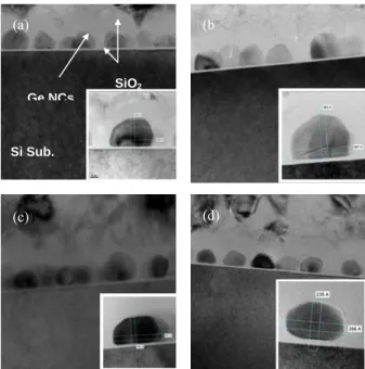
Figure 1 shows the scanning electron microscope (SEM) images taken from the Ge NCs formation after Fig. 1(c). A series of experiments are investigated in such conditions shown as Table I. The size of the Ge NCs is clearly larger as the growth duration increased (shown as Table I). We adjust the growth temperature and duration to obtain the maximum dot density to be 1.8 × 1010 cm-2. Compare to Fig. 2(b) and 2(d), we observe the size of Ge NCs is almost the same due to the faster growth rate at higher growth temperature. Fig. 3 shows the cross-sectional HRTEM image of the 120-min Ge NCs embedded in MOS capacitor for the as-deposited, 600oC, 800oC, and 950oC annealing samples. A high resolution image of one typical Ge NC is inserted for revealing the geometrical characteristics. It is clearly shown the as-deposited Ge NCs has been well-crystallized. Besides, we find the shape of the bigger Ge NCs was hemisphere-like due to the some small spherical Ge NCs combine to form bigger hemi-spherical Ge NCs. As annealing temperature increases, some of the Ge NCs aggress to each other, resulting in the formation of the bigger Ge NCs but we observe the Ge NCs do not diffuse somewhere seriously to be pushed down to the SiO2/Si interface. During
the 950oC annealing condition over its melting point, the Ge transfers from the liquid state to the solid state to rebuild the Ge NCs structure during quenching of the samples. However, the mean size and the density of the Ge NCs are not enough small and high, respectively. We
suggest the density of the Ge NCs is controlled by the first Step and the size of the Ge NCs is determined by the second step, such as gases flow, growth temperature and duration. Using exactly the same growth parameters, we have exposed the SiO2 surface without Si nuclei
to only GeH4 in the UHV/CVD system. We
find there are no exactly Ge NCs present on SiO2 surface observed by SEM.
Fig. 2. Cross-sectional HRTEM micrograph of the MOS capacitor containing Ge NCs. The inset shows an enlarged view of a Ge NC: (a) as-deposited and (b) 600oC (c) 800oC (d) 950oC annealing in N
2 ambien
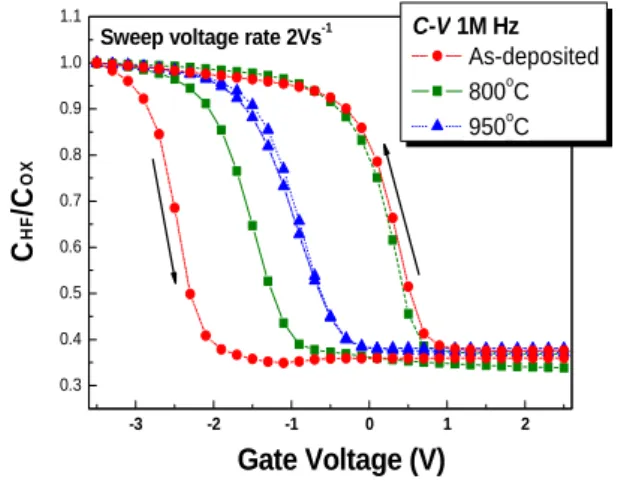
For C-V measurement, a HP4284A LCR meter is used. Fig. 5 shows typical high-frequency C-V characteristics of the MOS capacitor embedding Ge NCs grown for 120 min with as-deposited, 800oC annealing and 950oC annealing.
The measurements are performed at room temperature with a constant sweep rate of 2 Vs-1. It is seen that the devices yields a counter-clockwise hysteresis. All three samples are held for 30s at -3.5 V before being swept to
Si Sub. Ge NCs SiO2 (a) (b (c)) (d) (e)
2.5 V and then held at this voltage for 30s before returning to -3 V. The hold time ensures that the structure are fully charged or discharged by the holding bias before commencement of the voltage sweep. From the results of C-V curve, we observe the width of the hysteresis decreases significantly from the as-deposited sample to the 950oC-annealing sample at the same sweep bias range. We suggest the Ge NCs of the as-deposited sample have interfacial states or bulk deep traps to capture the electrons or holes. For the 800oC-annealing sample, the presence of unstable thermodynamically GeOx results in the
critical charge loss. Compare to as-deposited sample and 800oC annealing sample, it is shown the hole trapping effect is decreased during annealing. As to 950oC annealing sample, it indicates there is no hysteresis effect. After the high temperature annealing up to 950oC, the disappearance of the Ge-O bonds exhibits the improvement of the oxide quality. Also, the original interface states and bulk defects were annealed out. Maybe this is one of the reasons why there is no charge trapping in the high temperature annealing samples.
Fig. 3. HF-CV curves of the MOS capacitor embedding Ge NCs
grown for 120 min with as-deposited, 800oC-annealing and
950oC-annealing sample.
On the other hand, The fabrication process of Ge NCs using the E-gun system is as follows: The sample is fabricated by thermally grown 3nm-thick dry SiO2 layer as a tunneling oxide on
p-type (100) silicon substrate at 950oC after standard RCA recipes. Then, a Ge (a-Ge) layer is
deposited on the SiO2 layer by E-gun
evaporation. The following 40nm control oxide layer is grown by plasma enhanced chemical vapor deposition (PECVD). The three-layer structure (tunnel SiO2/Ge layer/Capping SiO2) is
then heated by furnace annealing treatment in a dry N2 ambient at 950oC for 300 seconds. This
treatment is in order to form well-separated Ge NCs. Last, 300nm Al contacts are deposited on both front and back surface to complete the gate stack formation of MOS capacitor. After evaporation, the sample is annealed at 4500C in either pure N2 or forming gas (90%N2+10%H2)
ambient as post-metallization-anneal (PMA) to investigate the effects of interface traps and defects inducing from the nanocrystals fabrication process.
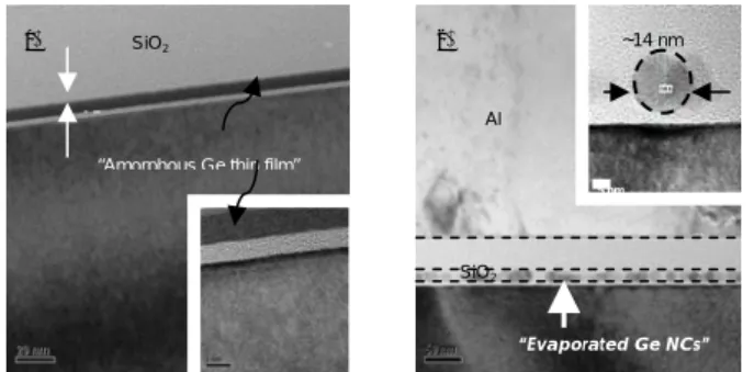
A cross-sectional TEM micrograph of a control oxide/Ge thin layer/tunnel oxide stack structure is shown in Fig. 4(a). From lack of lattice fringes shown in the inset of Fig.4(a),the Ge layer appears amorphous, as expected for an electron gun evaporated Ge film on room temperature. From TEM images, the thickness of Ge layer is about 4.5 nm. After annealing treatment at 950oC for 300 seconds in a dry N2
ambient, the crystalline Ge nanocrystals are formed in SiO2 matrix shown in Fig. 4 (b). The
lattice fringes is obviously shown in the inset images, which indicates the crystallization of the
whole amorphous layer at 950oC annealing
provides the enough thermal energy to
-3 -2 -1 0 1 2 0.3 0.4 0.5 0.6 0.7 0.8 0.9 1.0 1.1 C HF /C OX Gate Voltage (V) C-V 1M Hz As-deposited 800oC 950oC
agglomerate the Ge atoms due to high diffusivity of Ge atoms under heating. The Ge NCs size is about 14 nm
High frequency (1 MHz) C-V measurements are carried out using HP4284A impedance analyzer with various scanning range of gate bias in Fig. 5. Obviously, the counterclockwise hysteresis is widened by applying a higher gate voltage. The hysteresis is contributed by the trapping of charges in SiO2
during the scanning bias. In the experiment, MOS capacitor is first scanned between -1 and +1 V, and a small hysteresis (~0.1 V) is found, indicating little charging or discharging .After that, in the scanning of ±2V and ±3V, the wider hytsersises are observed about ~0.21V and
~0.48V. The insert is also shown the sweep
voltage increase up to 10 V, the hytsersis windows reaches to be ~8 V, respectively. This indicates that the charge storage capability of the structure increase with increasing the gate bias. Moreover, for further deliberating upon the detail charge mechanisms in Ge nanocrystals MOS capacitor and better understanding of the HF-C-V results, the frequency dependence of capacitance-voltage and conductance-voltage measurements under majority charged are
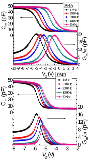
investigated (Fig.2). The measured capacitance (Cm) and the parallel measured conductance (Gm), normalized with angular frequency (ω=2πf) plot against gate voltage with frequency (f) ranging from 50 kHz to 1 MHz. In Fig.2, the upper data is Cm as a function of gate voltage and lower data is Gm/ω as a function of gate voltage. The device are first held at a gate voltage of -10 V for 30 seconds to ensure the positive charge storage, followed by a forward gate voltage sweep from -10 V to 10V. It is seen that the measured capacitance has the obvious frequency dispersion phenomenon with frequency. As the frequency decreases, the C-V shifts towards more positive voltage. This is a typical respond from exchange of charges between the NCs/traps to Si substrate. This causes an increase in total capacitance due to the additive effect of the capacitance due to NCs/traps. In addition, a strong measured conductance peak close to the flat band voltage is also observed during the G-V measurement, showing the existence of tunneling paths results in exchange of charges with a.c. signal modulation between the nanocrystals and the Si substrate.
Figure 5 High frequency C-V characteristics of evaporated Ge NCs embedded in MOS capacitor.
4 5
SiO2
“Amorphous Ge thin film”
(a) Al SiO2 “Evaporated Ge NCs” ~14 nm 5 nm (b)
Figure 4 (a) Cross-sectional HRTEM images of evaporated Ge NCs embedded in SiO2 for As-evaporated (amorphous Ge film ~ 4.5 nm) (b)
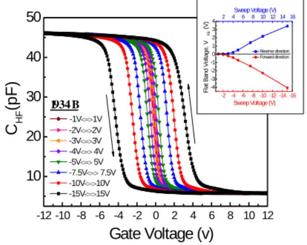
After PDA treatment at 950oC for 300 s in N 2 -14-12-10 -8 -6 -4 -2 0 2 4 6 8 10 12 14 10 20 30 40 50 -4 -6 -8-10 -12 -14 -16 -8 -6 -4 -2 0 2 4 6 4 6 8 10 12 14 16 Sweep Voltage (V) F la t B and V o lt ag e, V FB (V ) Sweep Voltage (V) Reverse direction Forward direction Gate Voltage, V G (v) C HF (pF) 1934 A (w/o PMA) -1V <=> 1V -2V <=> 2V -3V <=> 3V -4V <=> 4V -5V <=> 5V -7.5V <=> 7.5V -10V <=> 10V -15V <=> 15V
A post-metallization annealing (PMA) is performed on both the devices for 300 seconds at 400oC in a N2 ambient. The sample of 1934 A
with PMA treatment is called “1934 B”, respectively. Figure 6 shows the hysteresis of C-V relation in the evaporated Ge NCs devices with PMA treatment. An improvement of the stretch-out phenomenon in the C-V curves is observed on these two devices indicating possible passivation of interfacial traps between Ge NCs and surrounding oxide. Therefore, the PMA process reduces the interface states density and passivation of some dangling bonds in tri-layer structures. We suggest that the interfacial traps between Ge NCs and surrounding oxide is very close to the Si substrate observed from HRTEM images because evaporated Ge atoms aggressive each other and then ripens to form spherical-like Ge NCs during post-deposition annealing. The distance of Ge NCs and Si substrate becomes smaller than 3 nm. However, the window of hysteresis is not decreased by PMA treatment. This indicates the main mechanism of trapping electrons or holes is not due to the interfacial traps.
Figure 6 High frequency C-V characteristics of evaporated Ge NCs
embedded in MOS capacitor for 1934 B samples.
In order to further understand the involved shallow traps, the C-V, G-V technique with different frequencies is used to measure the devices since the associated trap characteristic is frequency-dependent. The frequency-dependent
C-V and G-V characteristics are measured at
frequency between 50KHz and 1000KHz with a small-amplitude (50mV) sine-wave voltage (AC) signal and the DC bias ranging from -10V to 10V. The measured apparent capacitance (Cm) and parallel apparent conductance (Gm) over the angular frequency (ω=2πf) versus the gate voltage with different frequency are shown in the top and bottom plots of Figs. 7(a) and (b) for Samples 1934A and 1934B which are directly obtained by HP 4284 A LCR meter respectively. It is seen that the Cm and Gm both shift towards much more positive bias for Sample 1934A than
1934B. In addition, the Gm magnitude is
suppressed by PMA treatment for Sample B, especially at low frequency. It is also attributed to PMA treatment curing the traps and reducing the leakage current.
In addition, strong measured conductance peak close to the flat band voltage are also
observed during the Gm-V measurement in
bottom data of Fig. 7(a) and (b), respectively, corresponding to the respective Cm-V curves
while the Gm-V curves of sample A are
strench-out relating to Cm-V curves, the Gm-V curves of sample B are comparatively sharp, showing the existence of tunneling paths results in exchange of charges with AC signal between traps and Si substrate. The peak of Gm-V curves are shifted according to flat band voltage shift of
Cm-V curves. And the peak shifting is considered as different traps states throughout the silicon
-12 -10 -8 -6 -4 -2 0 2 4 6 8 10 12 10 20 30 40 50 -2 -4-6-8 -10 -12 -14 -16 -4 -3 -2 -1 0 1 2 3 4 2 4 6 8 10 12 14 16 Sweep Voltage (V) Fl at Ba nd Vo lta g e , V FB (V ) Sweep Voltage (V) Reverse direction Forward direction Gate Voltage (v) CHF (pF) 1934 B -1V<=>1V -2V<=>2V -3V<=>3V -4V<=> 4V -5V<=> 5V -7.5V<=> 7.5V -10V<=>10V -15V<=>15V
band, which produce a conductance peak at different Fermi level positions under different frequency. On the other hand, comparing to
Cm-V characteristics of the samples, the wider peak shifts, larger magnitudes and broadening FWHMs are found in sample A, these phenomena are believed as a lot of defects existence in the defective oxide and surface states between Ge NCs or substrate. These defects offer more energy loss paths and energy trap levels to contribute the conductance characteristics.
Fig. 7 The measured capacitance and the parallel measured conductance VS. the gate voltage with frequency as parameter for 1934 A and 1934 B sample. It is clearly shows the smaller frequency dispersion
phenomena for the 1934 B sample.
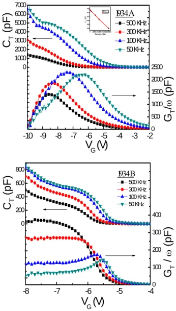
For further deliberating upon the detail traps characteristics and mechanisms, the measured apparent capacitance and conductance of the MOS structure with embedded Ge NCs are used to find the associated trap capacitance and trap conductance. If we assume the position of NCs/trap is close enough to that of Si/SiO2
interface, then the detailed equivalent circuit can be approximated as that shown in Fig.4. and the trap model derived by Nicollian and Goetzgergen used in the MOS structure can still be utilized here. In the Fig. 4, the series resistance, Rs, is approximated by the bulk and back contact resistance, which is bias-dependent. Series resistance can cause an error in the extraction of substrate admittance from admittance measurements. The oxide
capacitance, Cox is found as maximum
capacitance in strong accumulation region. And,
Cd is depletion layer capacitance, CT is the trap capacitance, GT is the trap conductance.
From the Shockley-Read-Hall (SRH) theory with the small signal approximation for trap model throughout the depletion region in considering majority carriers (holes), the trap admittance, YT, is given by the following expression:[12] T T T
G
j
C
A
j
A
Y
ω
ωτ
ω
τ
ω
=
+
+
+
=
2 2)
(
1
(1) where ω is measured frequency, τ is the characteristic time constant, GT is the trap conductance represents the loss process of capture-emission carriers by traps, CT is the trap capacitance. Trap admittance consists of the trap conductance shunted by the trap capacitance.-8 -7 -6 -5 -4 -3 -2 -50 -40 -30 -20 -10 0 10 20 30 40 50 0 4 8 12 16 20 24 28 32 1934 B 1 MHz 500 KHz 300 KHz 100 KHz 50 KHz
G
m/
ω(p
F)
C
m(pF)
V
G(V)
-10-9 -8 -7 -6 -5 -4 -3 -2 -1 0 1 2 3 4 -50 -40 -30 -20 -10 0 10 20 30 40 50 0 5 10 15 20 25 30 35 40 G m / ω (pF) C m (pF) VG (V) 1934 A 1 MHz 500 KHz 300 KHz 100 KHz 50 KHzTherefore, 2
)
(
1
+
ωτ
=
A
C
T (2)τ
ω
ωτ
τ
ω
2 2 2 ) ( 1 T T C A G = + = (3)To extract the trap admittance, the real series resistance (Rs) of MOS devices is subtracted
from the measured capacitance (Cma) and
conductance (Gma) in strong accumulation region.
The oxide capacitance (Cox) is found as
maximum capacitance in strong accumulation region at the given frequency. [12] Eliminating the Rs and Cox effect, the equivalent parallel capacitance (Cp) shunted with the equivalent parallel conductance (Gp) are obtained. The Cp consists of the depletion layer capacitance (Cd) and the trap capacitance (CT) can be expressed parallel as Cp= Cd + CT. Also, the trap conductance, GT is the same as the equivalent parallel conductance Gp=GT. At enough high frequency (~1000KHz), it is assumed that the contribution of trap capacitance to the total capacitance is negligibly small because charges exchange between NCs/traps and Si substrate cannot follow the AC signal approximately. Consequently, at 1000KHz the trap capacitance,
CT(ω) is determined as CT = 0 for reference state. In addition, the deep trap contribute to the capacitance is also disregarded due to its maintaining the same hysteresis windows under various measured frequency. So under these assumptions, the depletion layer capacitance is approximately subtracted from 1000KHz measured capacitance.
Figure 8 The trap capacitance and the parallel trap conductance VS. gate voltage for 1934 A sample and 1934 B sample. It is clearly shown trap capacitance is suppressed by PMA process due to recovery of defects. The inset of figure shows the Cox value at ω=0 is extrapolated
from Cox VS. f curve
The trap capacitance (CT) and the parallel trap conductance (GT) normalized with angular frequency as functions of gate voltage of sample A and B are extracted from the measured apparent Cm-V and Gm-V shown in Fig. 8. The result of sample 1934A from the top plots in Fig. 8(a), we can observe the trap capacitance variations by different gate bias and measured frequency. Obviously, the trap capacitance is represented the decrement as measured
-10 -9 -8 -7 -6 -5 -4 -3 -2 -7000 -6000 -5000 -4000 -3000 -2000 -1000 0 1000 2000 3000 4000 5000 6000 7000 0 500 1000 1500 2000 2500 3000 3500 4000 4500 5000
V
G(V)
G
T/
ω(p
F)
C
T(pF)
1934 A 500 KHz 300 KHz 100 KHz 50 KHz 0250000 500000 7500001000000 48.6 48.8 49.0 49.2 49.4 49.6 Cox (pF ) Frequency, f (Hz) 1934 Extrapolated -8 -7 -6 -5 -4 -800 -600 -400 -200 0 200 400 600 800 0 100 200 300 400 500 600 700G
T/
ω(pF)
C
T(pF)
V
G(V)
1934 B 500 KHz 300 KHz 100 KHz 50 KHzfrequency increasing. This phenomenon is explained by changing the DC bias, the silicon Fermi level can be moved through the energy levels in the Ge NCs or the interfacial traps, once the Fermi level is aligned with the energy level in Ge NCs or traps while measured frequency is slow enough to prompt the carriers keeping up with AC signal, the carriers can be synchronized between the Ge NCs/traps and Si substrate with AC signal and yield an excess capacitance. Therefore, at low modulation frequency the charges distributed in high energy level and deeper energy level all follow the AC signal to allow more exchange charges to achieve larger trap capacitance. Besides, another important point of the trap capacitance versus gate voltage characteristics is that the trap capacitance as function of gate voltage is very broad. This is resulted from the broad energy level distribution of Ge NCs caused by size fluctuations or traps around Ge NCs. In addition, the huge increment in the trap capacitance at a higher negative bias might come from the higher energy levels in Ge NCs or traps because the charges which resides in the higher energy levels.Lastly, in top plots in Fig. 8(b); the sample 1934B which is treated by PMA, its extracted value of trap capacitance is dramatically reduced and frequency dispersion is also strongly suppressed. The result is also consisted with previous high frequency C-V hysteresis with PMA effect that atomic hydrogen can effectively passivate the dangling bonds and shallow interfacial traps.
四、結論與討論
In this work, we present an extensive study about the formation of Ge nanocrystals, including chemical and physical vapor
deposition. First, Ge nanocrystals formation by using UHV/CVD system is used a two-step process as follows: The first step is Si
pre-growth seeding: the SiO2 surface is
randomly functionalized by the deposition of Si nuclei using SiH4 flow. The second step is Ge
dot growth: once the Si nuclei are deposited, we stop the SiH4 gas flow, and GeH4 is introduced
to selectively grown on the Si nuclei. We control
SiH4 and GeH4 flow rate, the furnace
temperature at 550oC or 600oC. Among different growth temperature and duration, the diameter of Ge dot could be controlled between 20 nm and 130 nm. The maximum density of Ge NCs is adjustable to be 1.8E10 cm-2.
Then, the tri-layer structure (control oxide/Ge NCs/tunnel oxide) is treated by post-deposition annealing at 500 oC ~ 950 oC for 20 min in a dry N2 ambient. We find the oxide
quality is improved during high temperature annealing. The capacitance-voltage hysteresis shows the charge storage effect in MOS capacitor with embedded CVD Ge NCs. The memory window shows a maximum value for as-deposited sample, and then decreases with higher annealing temperature up to 950 oC. However, the charge retention time is also related with annealing temperature. A maximum memory window of 2.6 V is observed after 104 seconds in the 950 oC annealed sample. The 950
oC annealed sample also shows the lowest charge
loss rate of ~ 46%.
Another fabricating method of Ge NCs is formed by furnace annealing of an evaporated, ultra-thin Ge layer at 900 oC for 300 s in a N2
ambient followed by a N2 ambient. C-V
measurements show the amount of electrical charges (electrons or holes) which can be stored
or trapped in the devices varies with the thickness of a-Ge thin films. The larger coverage rate of Ge NCs on tunnel oxide surface which results from thick a-Ge thickness causes the larger amount of charges stored in the devices. Comparison between the devices with PMA treatment and without PMA treatment, the devices with PMA treatment shows better retention characteristic of and lower charge loss rate.
We also propose a single trap model based on SRH theory by introducing another charge loss time constant in this model. In our work, we utilize our trap model to compare the charge retention characteristics between the devices with/without PMA treatment. From the measured admittance, we extract the values of trap capacitance and trap conductance. Trap capacitance in the device without PMA treatment is larger than that with PMA treatment. We suggest the defects or surface states around Ge NCs are annealed out by PMA treatment, resulting in smaller amount of communication of charges between NCs/traps caused by the reduction of conductive paths. In addition, the amount of trap conductance is also reduced. The charge loss time constant for the devices with PMA treatment is larger than that for the device without PMA treatment due to the reduction of surface state density or oxide defectd around Ge NCs caused by PMA treatment, resulting in the suppression of trap-assisted tunneling through the tunnel oxide to decrease the charge loss behavior. During PMA treatment, the shallow traps in the oxide are annealed out, resulting in reduction of trap capacitance and trap conductance but the charge retention is not obviously improved due to the charges storing in
the deeper traps or deeper potential well.
五、參考文獻
[1] Y.-C. King, T.-J. King, and C. Hu, “Charge-trap memory device fabrication by oxidation of Si1-XGeX,” IEEE Trans.
[2] W. K. Choi, V. Ng, S. P. Ng, H. H. Thio, Z. X. Shen and W. S. Li, “Raman characterization of germanium nanocrystals in amorphous silicon oxide films synthesized by rapid thermal annealing,” J. Appl. Phys., vol. 86, no. 3, pp. 1398-1403, 1999.
[3] K. S. Min, K. V. Shcheglov, C. M. Yang, H. Atwater, M. L. Brongersman and A. Polman, “ The role of quantum-confined excitons vs defects in the visible luminescence of SiO2 films containing Ge nanocrystals,”
Appl. Phys. Lett., vol. 68, pp. 2511-2513, 1996.
[4] G. Taraschi, S. Sanini, W. W. Fan, L. C. Kimerling,and E. A. Fitzgerald, “Nanostructrue and infrared photo-luminesence of nanocrystalline Ge fomed by reduction of Si0.75Ge0.25O2/ Si0.75Ge0.25 using various H2
pressures,” J. Appl. Phys., vol. 93, no. 12, pp. 9988-9996, 2003.
[5] C. L. Heng, W. W. Tjiu, and T. G. Finstad, “Charge-storage effects in a metal-insulator-semiconductor structure containing germanium nanocrystals formed by rapid thermal annealing of an electron-beam evaporated germanium layer;” Appl. Phys. A : Material Science &
Processing, vol. 78, pp. 1181-1186, 2004
[6] D.-W. Kim, S. Hwang, T. F. Edgar, and S. Banerjeea, “Characterization of SiGe quantum dots on SiO2 and HfO2
grown by rapid thermal chemical deposition for nanoelectronic devices,” J. Electrochem. Soc., vol. 150, no. 4, 2003
[7] J. H. Chen, Y. Q. Wang, W. J. Yoo, Y.-C. Yeo, Ganesh, D. SH Chan, A. Y. Du, and D.-L. Kwong, “Nonvolatile Flash Memory Device Using Ge Nanocrystals Embedded in HfAlO high-k Tunneling and control oxide: Device Fabrication and Electrical performance,” IEEE Trans.
[8] T. Baron, B. Pelissier, L. Perniola, F. Mazen, et al., “Chemical vapor deposition of Ge nanocrystals on SiO2,”
Appl. Phys. Lett., vol. 83, no. 7, pp. 1444-1446, 2003.
[9] B.S. Meyerson, “low-temperature silicon epitaxy by ultra-high vacuum/ chemical vapor deposition,” Appl.