國 立 交 通 大 學
電子物理學系
碩士論文
新穎堆疊矽/鍺 T 型閘極複晶矽薄膜電晶體
A Novel Poly-Silicon Thin-Film Transistors with
Stacked Si/Ge T-Gate
研 究 生:謝佩珊
指導教授:趙天生 博士
新穎堆疊矽/鍺 T 型閘極複晶矽薄膜電晶體
A Novel Poly-Silicon Thin-Film Transistors with Stacked
Si/Ge T-Gate
研 究 生:謝佩珊 Student:Pei-Shan Hsieh
指導教授:趙天生 博士 Advisor:Tien-Sheng Chao
國 立 交 通 大 學
電子物理學系
碩士論文
A Thesis
Submitted to Department of Electrophysics
National Chiao Tung University
In partial Fulfillment of the Requirements
For the Degree of Master of Science
In
Electrophysics
June 2006
HsinChu, Taiwan, Republic of China
新穎堆疊矽/鍺 T 型閘極複晶矽薄膜電晶體
研究生:謝佩珊 指導教授:趙天生 博士
國立交通大學
電子物理學系
摘要
多晶矽薄膜電晶體擁有高載子遷移率目前被廣泛地運用在主動矩陣式液晶顯示器開 關元件,然而,在汲極端產生的強電場會造成嚴重漏電流和元件不穩地性,將會阻礙多 晶矽薄膜電晶體在高效能積體電路的應用。造成漏電的主要因素是由於在汲極端附近的 強電場經由顆粒邊界的受限載子引起場發射而使漏電上升。 在本論文中,我們針對多晶矽薄膜電晶體提出新的製程方法,此製程簡單無需額外 的光罩,或是離子佈植步驟,即可形成堆疊矽/鍺T型閘極元件,期可達到抑制電場效果。 利用模擬軟體來分析證明,藉由T型閘極可有效降低汲極端附近的電場。 我們對於堆疊矽/鍺T型閘極複晶矽薄膜電晶體,探討其元件特性,包括傳輸性能、 開/關電流比、漏電強度、輸出性能,以及熱載子可靠度分析。由結果顯示,堆疊矽/鍺 T型閘極複晶矽薄膜電晶體,可使漏電流降低,並提升開/關電流比,此外Kink效應及熱 載子可靠度也明顯優於傳統元件。
A Novel Poly-Silicon Thin-Film Transistors with
Stacked Si/Ge T-gate
Student:Pei-Shan Hsieh Advisors:Dr. Tien-Sheng Chao
Department of Electrophysics
National Chiao Tung University
Abstract
Polycrystalline silicon thin-film transistors (poly-Si TFTs) are commanding increasing interest in the field of active matrix addressed flat panel display because the higher carrier mobility in this material compared with a-Si:H TFTs, which makes it suitable for the integration of addressing circuits in the displays. However, a large off-state leakage current and device instability caused by a high electric field near the drain junction are obstacles to the high-performance circuit application of the poly-Si TFTs. The dominant mechanism of the high off-state leakage current is known to be the field emission via grain boundary traps due to a high electric field in the drain depletion region.
In this thesis, we have proposed a new fabrication method of poly-Si TFT without a troublesome ion implantation or any additional mask. This device employs the stacked Si/Ge T-Gate to suppress the electric field. It was verified by the devices simulator that the electric field is reduced near the drain junction by the T-Gate structure.
including the transfer characteristics, On/Off current ratio, off -state leakage, output characteristics and hot carrier stress. The results show that the Si/Ge T-Gate TFT give low off-state leakage, the suppress of floating body effect, good On/Off current ratio and better hot carrier reliability.
誌謝
兩年短暫的碩班生活,匆匆走過卻不虛此行,而此論文也為求學生涯畫下短暫的句 點。一路走來,受到許多人的關心幫助,在此表達感謝之意。首先要感謝指導教授趙天 生老師在學業及實驗上給予最大的支持與協助,此外在為學處世及待人接物上也都讓我 有相當多啟發。此外,我要特別感謝東海大學的蕭錫鍊老師,大學兩年的專題指導,讓 我更早認知研究生態,及學習實驗研究精神。 再者要特別感謝郭柏儀學長,在實驗、研究上熱心無私的指導,使我獲得許多寶貴 的實驗經驗,而學長的認真執著的研究精神,也是我永遠的學習榜樣。此外,也感謝當 初和我們同時進入實驗室的吳偉成學長,絕佳領導風範及特別的人生哲學,讓我有更開 闊的視野及想法。另外,還要感謝浪費寶貴時間聽我們報告的羅文政學長,告訴我們許 多人生道理的李耀仁學長,熱心認真的吳家豪學長,以及協助我找到好工作的張宗憲學 長,有大家這一路的提攜照顧,實在感激不盡。 同時,也要謝謝竣祥、彥學、武欽、棟煥,有幸能夠當同學,一起上課、做實驗、寫論 文,度過充實的兩年,真的非常有緣。另外也要感謝可愛搞笑的學弟妹,美君、國興、 宗諭、德馨、宜憲、妍心、明宏、家塵,枯燥單板的碩班生活,有了妳們的加入,讓實 驗室常常充滿歡笑,也讓我的回憶更加美好精采,然而也要特別謝謝宗諭,在實驗模擬 上的幫忙,使我的論文更加完整。 感謝國家奈米元件實驗室和交通大學奈米中心在儀器設備上的支援,以及每位工程 師在製程上的幫忙。對於諸位口試委員的建議與指證也表感激之意。 最後,我要對我的父母表達我最深的敬意及感謝,二十多年來,辛苦工作省吃儉用, 讓我擁有優良的讀書環境,無怨無悔地付出,令我非常感激,還有非常感謝我摯愛的弟 弟、妹妹,在人生路上的陪伴支持與鼓勵。Contents
Abstract (Chinese)………I
Abstract (English)………II
Acknowledge………...IV
Contents………V
Table captions………VII
Figure captions……….VIII
Chapter 1 Introduction……….1
1.1 Overview of Thin-Film Transistor Technology………....1
1.2 Motivation……….... 2
1.3 Thesis Outline……….. 3
Chapter 2 Experimental Process and Electrical Parameters Extraction….
……… 5
2.1 Fabrication of the thin-film transistors (TFTs)……….... 5
2.1.1 Fabrication of the Si/Ge T-Gate TFTs………...5
2.1.2 Fabrication of the Conventional TFTs……….. 6
2.2 Method of device parameter extraction………... 8
2.2.1 Threshold Voltage (VTH)………... 8
2.2.2 Subthreshold Swing (S.S.)……….. 8
2.2.3 On/Off Current Ratio………... 9
2.3 Material analysis………... 10
Chapter 3 Electrical Characterization of the Si/Ge T-Gate TFTs... 17
3.1 Device Simulation………. 17
3.2.1 Transfer Characteristics……….... 18
3.2.2 On /Off Current Ratio………... 20
3.2.3 Off -State Leakage……….... 21
3.2.4 Output Characteristics………... 21
3.2.5 Hot Carrier Stress………... 23
Chapter 4 Conclusions and Future Works……… 64
4.1 Conclusions……….64
4.2 Future Works………...65
Table Captions
Chapter 2
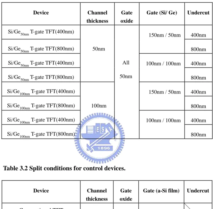
Table2.1 Split condition for all samples with different thickness of stacked Si/Ge and undercut length.
Figure Captions
Chapter 2
Fig.2.1 The schematic cross section of the Si/Ge T-gate TFTs with TEOS passivation Fig.2.2 The schematic cross section of the Si/Ge T-gate TFTs with Si3N4 passivation
Fig.2.3 The schematic cross section of conventional TFTs Fig.2.4 Process flows of Si/Ge T-gate TFTs.
Chapter 3
Fig.3.1 Stacked Si/Ge gate with the germanium undercut structure observed by cross section TEM microphotographs.
Fig.3.2 Thickness of channel film, gate oxide, gate, and undercut length are shown in this picture.
Fig.3.3 SEM image of the Stacked Si/Ge gate with undercut structure.
Fig.3.4 The simulated lateral electric field along the channel (10μm) direction near the drain the VG= -10V, VD= 10V. The different stacked Si/Ge gate thichness with
TEOS passivation of (a) Undercut length is 400nm. (b) Undercut length is 800nm. Fig.3.5 The simulated vertical electric field along the channel (10μm) direction near the
drain the VG= -10V, VD= 10V. The different stacked Si/Ge gate thichness with
TEOS passivation of (a) undercut length is 400nm. (b) undercut length is 800nm. Fig.3.6 The simulated lateral electric field along the channel (10μm) direction near the
drain the VG= 0V, VD= 15V. The different stacked Si/Ge gate thichness with TEOS
passivation of (a) undercut length is 400nm. (b) undercut length is 800nm. Fig.3.7 The simulated vertical electric field along the channel (10μm) direction near the
drain the VG= 0V, VD= 15V. The different stacked Si/Ge gate thichness with TEOS
Fig.3.8 The simulated lateral electric field along the channel (10μm) direction near the drain the VG= -10V, VD= 10V. The different stacked Si/Ge gate thichness with
SiNx passivation are shown.
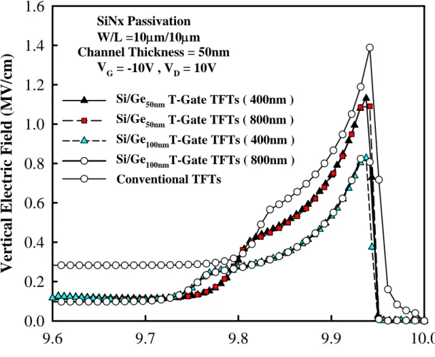
Fig.3.9 The simulated vertical electric field along the channel (10μm) direction near the drain the VG= -10V, VD= 10V. The different stacked Si/Ge gate thichness with
SiNx passivation are shown.
Fig.3.10 The simulated lateral electric field along the channel (10μm) direction near the drain the VG= 0V, VD= 15V. The different stacked Si/Ge gate thichness with SiNx
passivation are shown.
Fig.3.11 The simulated vertical electric field along the channel (10μm) direction near the drain the VG= 0V, VD= 15V. The different stacked Si/Ge gate thichness with SiNx
passivation are shown.
Fig.3.12 The transfer characteristics of the Si/Ge T-Gate TFTs with different thickness of stacked Si/Ge and undercut length. The channel thickness is 50nm and gate length is 5μm.
Fig.3.13 The transfer characteristics of the Si/Ge T-Gate TFTs with different thickness of stacked Si/Ge and undercut length. The channel thickness is 50nm and gate length is 8μm.
Fig.3.14 The transfer characteristics of the Si/Ge T-Gate TFTs with different thickness of stacked Si/Ge and undercut length. The channel thickness is 50nm and gate length is 5μm.
Fig.3.15 The transfer characteristics of the Si/Ge T-Gate TFTs with different thickness of stacked Si/Ge and undercut length. The channel thickness is 50nm and gate length is 3μm.
Fig.3.16 The transfer characteristics of the Si/Ge T-Gate TFTs with different thickness of stacked Si/Ge and undercut length. The channel thickness is 100nm and gate
length is 10μm.
Fig.3.17 The transfer characteristics of the Si/Ge T-Gate TFTs with different thickness of stacked Si/Ge and undercut length. The channel thickness is 100nm and gate length is 8μm.
Fig.3.18 The transfer characteristics of the Si/Ge T-Gate TFTs with different thickness of stacked Si/Ge and undercut length. The channel thickness is 100nm and gate length is 5μm.
Fig.3.19 The transfer characteristics of the Si/Ge T-Gate TFTs with different thickness of stacked Si/Ge and undercut length. The channel thickness is 100nm and gate length is 3μm.
Fig.3.20 The transfer characteristics of the Si/Ge T-Gate TFTs with different thickness of stacked Si/Ge and undercut length. The channel thickness is 50nm, gate length is 10μm.
Fig.3.21 The transfer characteristics of the Si/Ge T-Gate TFTs with different thickness of stacked Si/Ge and undercut length. The channel thickness is 50nm, gate length is 8 μm.
Fig.3.22 The transfer characteristics of the Si/Ge T-Gate TFTs with different thickness of stacked Si/Ge and undercut length. The channel thickness is 50nm, gate length is 5 μm.
Fig.3.23 The transfer characteristics of the Si/Ge T-Gate TFTs with different thickness of stacked Si/Ge and undercut length. The channel thickness is 50nm, gate length is 3μm.
Fig.3.24 Gate length dependence of On/ Off current ratio in Si/Ge T-gate TFTs with TEOS passivation and conventional TFT. (a) The channel thickness is 50nm (b) The channel thickness is 100nm.
passivation and conventional TFT.
Fig.3.26 Off-state leakage Characteristics in Si/Ge T-gate TFTs with TEOS passivation which compared with conventional TFT. (a) The channel thickness is 50nm (b) The channel thickness is 100nm.
Fig.3.27 Off-state leakage Characteristics in Si/Ge T-gate TFTs with Si3N4 passivation
which compared with conventional TFT.
Fig.3.28 The output characteristics of the Si/Ge T-Gate TFTs with TEOS passivation. The channel thickness is 50nm. (a) Germanium layer thickness is 50nm (b)
Germanium layer thickness is 100nm.
Fig.3.29 The output characteristics of the Si/Ge T-Gate TFTs with TEOS passivation .The channel thickness is100nm. (a) Germanium layer thickness is 50nm (b)
Germanium layer thickness is 100nm.
Fig.3.30 The output characteristics of the Si/Ge T-Gate TFTs with Si3N4 passivation. The
channel thickness is 50nm. (a) Germanium layer thickness is 50nm (b) Germanium layer thickness is 100nm.
Fig.3.31 Stress time dependence of Ion variation in Si/Ge T-Gate TFTs and conventional
TFT. (a) Channel length is 10μm. (b) Channel length is 5μm.
Fig.3.32 Variations of the threshold voltage under hot carrier stress in conventional TFT and Si/Ge T-Gate TFTs. (a) Channel length is 10μm. (b) Channel length is 5μ m.
Chapter 4
Fig.4.1 The schematic cross section of stacked Si/Ge T-Gate TFT with O/N/O tripping layer.
Chapter 1
Introduction
1.1. Overview of Thin-Film Transistor Technology
A thin film transistor (TFT) is defined as a field-effect transistor built using a semiconductor thin film which is originally deposited on an insulating material [1].We usually use the amorphous-Si and poly-Si as the thin film materials.
Most of TFT-LCD products were fabricated using a-Si:H TFTs as the pixel devices because of their advantages, such as low processing temperature (<350°C), good compatibility with large area glass substrate, simple process, and low leakage current, which is suitable for pixel switching. However, a-Si:H TFT’s have some inherent undesirable properties. First of all, its carrier mobility is extremely low (typically below 1 cm2/V-s), which will prohibit the integration of driver circuitry on the active matrix plate. Furthermore, the quality of gate dielectric and oxide-poly interface is not good enough because of the low temperature process. Therefore, the mobile carriers from the source may somewhat leak to gate terminal or suffer lots of scatterings at the interface during the transport process. As the display area and pixel density of TFT-LCD are increasing, the TFT-LCD pixel driver needs to use high mobility in order to shorten the charging time of pixel electrodes. It is very difficult for a-Si:H TFT because of its low carrier mobility.
Recently, polycrystalline silicon thin-film transistors (poly-Si TFTs) are commanding increasing interest in the field of active matrix addressed flat panel display because the higher carrier mobility in this material, compared with a-Si:H TFTs, makes it suitable for the integration of addressing circuits in the displays.[2] In comparing poly-Si devices with their single-crystal counterparts, the main difference in their characteristics arises because of the
presence of grain boundaries in the poly-Si, which will affects the device performances including the on-state current, threshold voltage, and field-effect mobility. In addition, these defects also generate junction leakage current at the source and drain which increases the off-state leakage current.[3][4] The off-state leakage current has been found to increase exponentially with increasing different between gate and drain voltage, and has been attributed to the field emission of carriers via the traps by high electric-field near the drain junction.[5][6][7]
Recently, dozens of researches have been made to develop various technologies for improving the performance and reliability of LTPS TFTs. Poly-Si films crystallized from a-Si usually results in a larger grain size has been considered the most important process for fabrication high-performance LTPS TFTs. Many techniques about crystallization of amorphous silicon, such as solid phase crystallization (SPC)[10][11], excimer-laser annealing (ELA)[12][13], rapid thermal annealing (RTA)[14][15], metal induced lateral crystallization (MILC)[16][17], have been proposed. However, other low-temperature process technologies in the procedure of fabricating LTPS TFTs, such as gate dielectric formation, thin film deposition, ion doping/dopant activation, defect passivation, lithography, and etching are also indispensable for producing high-performance LTPS TFTs. [18]
1.2. Motivation
In poly-Si film, carrier mobility large than 10 cm2/Vs can be easily achieved, that is enough to used as peripheral driving circuit including n- and p-channel devices.[17][18] For the drive circuits, the carrier field effect mobility is a key issue, but for the pixel TFT the leakage current is the major concern. Before poly-Si can be used for the switching transistor, a leakage current must be reduced below 1pA. [19]
known to present several undesired effects, including large off-current [20], kink effect [21] and electrical instabilities induced by hot-carrier effects (HCEs) [22][23]. The dominant mechanism of the high off-state leakage current is known to be the field emission via grain boundary traps due to a high electric field in the drain depletion region [24][25].
In order to reduce the abovementioned effects, a poly-Si TFT with an offset gate, a lightly doped drain (LDD), and a field-induced drain structure have been widely used to reduce the drain electric field. [26][27][28][29] Since the offset region between gate and source/drain suppresses the drain electric field, the offset gated poly-Si TFT has a low off-state leakage current. However, these structures inevitably decrease the on-state current due to the extra series resistance of the offset region is a serious problem. To alleviate this problem, an additional step of spacer formation followed by implantation is employed. Although a poly-Si TFT with LDD has better turn-on characteristics than an offset-gated TFT, device degradation due to implant damage and difficulty in doping control at the grain boundaries are important issues.[30] A poly-Si TFT with field-induced drain (FID) have high ON/OFF current ratio, because this structure can effectively reduce the drain electric field and is free from implant damage.[31] Compared with LDD structure, the FID structure is attractive obviously because it can overcome the shortcomings existed in LDD approach.
In the thesis, the novel poly-Si thin film transistor with stacked Si/Ge T-gate is proposed and experimentally demonstrated. The process dose not require any additional mask step or ion implantation process. It is found that this device structure provides low off-state leakage current compared with the conventional TFTs by reduced the electric field near the drain junction.
1.3. Thesis Outline
In this thesis, experimental process and electrical parameters extraction are shown in chapter 2. Inchapter 3, the electrical characterization of the Si/Ge T-gate TFTs are compared
with the conventional TFT.In chapter 4, the conclusions of this thesis and the future work are given.
Chapter 2
Experimental Process and Electrical Parameters Extraction
2.1 Fabrication of the thin-film transistors (TFTs)
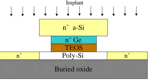
The schematic cross sections of the Si/Ge T-Gate TFT is shown in Fig.2.1 and Fig.2.2.
And the schematic cross section of conventional device is shown in Fig.2.3. The fabrication procedures of these devices are described as following (Fig.2.4):
2.1.1 Fabrication of the Si/Ge T-Gate TFTs
I. Substrate:
The 6-in single crystalline silicon wafers with (100) orientation were used as the starting materials. After an RCA initial cleaning procedure, 550 nm thick thermal oxide was grown in steam oxygen ambient at 980°C.
II. Poly-Si thin film active region formation:
Undoped amorphous silicon layers of thickness about 50/100nm were deposited by low pressure chemical vapor deposition (LPCVD) on buried oxide by hydrolysis of silane (SiH4)
at 550°C. Then, the amorphous silicon films were recrystallized by solid phase crystallization (SPC) method at 600°C for 24 hrs in an N2 ambient. These recrystallized poly silicon films
were then patterned into active region islands by transformer couple plasma (TCP) etching using the mixture of Cl2 and HBr.
III. Gate dielectric and gate electrode formation:
After defining the active region, the 50nm thick gate TEOS oxide was deposited by low pressure chemical vapor deposition (LPCVD). Then, the germanium layer and the a-Si layer
were deposited as a gate, as shown Table 2.1. Table 2.2 shows the conditions for control devices.
Then, the wafers were ion implanted by phosphorous. The energy and the dose of implantation were 60keV and 5E15cm-2. After the ion implantation, the germanium film and the a-Si layer were patterned and etched by transformer couple plasma (TCP-9400) to be the gate electrode.
IV. Si/Ge T-gate structure formation:
The T-gate was etched by selective wet etch method to form a T-shape structure. Then, Source and drain region were implanted by phosphorus (P) at 15keV /25keV to a dose of 5E15 cm-2.
V. Passivation layer and contact metal:
Following, 300nm thick TEOS oxide by LPCVD was deposited and the contact hole was defined. TEOS oxide was etched by buffer oxide etchant (BOE) dip. Then, 500nm Aluminum sputtering and defines the metal pad. After etching Aluminum, the device was finished.
The nitride was also used to be a passivation material compare with the TEOS passivation device. In the chapter3, the electrical characteristics of the Si/Ge T-gate TFTs with Si3N4
passivation would compare with the TEOS passivation device.
2.1.2 Fabrication of the conventional TFTs
I. Substrate:
The 6-in single crystalline silicon wafers with (100) orientation were used as the starting materials. After an RCA initial cleaning procedure, 550 nm thick thermal oxide was grown in steam oxygen ambient at 980°C.
II. Poly-Si thin film active region formation:
Undoped amorphous silicon layers of thickness about 50/100nm were deposited by low pressure chemical vapor deposition (LPCVD) on buried oxide by hydrolysis of silane (SiH4)
at 550°C. Then, the amorphous silicon films were recrystallized by solid phase crystallization (SPC) method at 600°C for 24hrs in an N2 ambient. These recrystallized poly silicon films
were then patterned into active region islands by transformer couple plasma (TCP) etching using the mixture of Cl2 and HBr.
III. Gate dielectric and gate electrode formation:
After defining the active region, the 50nm thick gate TEOS oxide was deposited by low pressure chemical vapor deposition (LPCVD). Then, the 200nm a-Si film was deposited immediately on the gate dielectric by LPCVD at 550°C. (Table2)
Then, the wafers were ion implanted by phosphorous. The energy and the dose of implantation were 60 keV and 5E15 cm-2. After the ion implantation, the a-Si layer were patterned and etched by transformer couple plasma (TCP-9400) to be the gate electrode.
IV. Source/Drain region formation:
Source and drain region were implanted by phosphorus (P) at15 keV /25 keV to a dose of 5E15 cm-2.
V. Passivation layer and contact metal:
Following, 300nm thick TEOS oxide by LPCVD was deposited and the contact hole was defined. TEOS oxide was etched by buffer oxide etchant (BOE) dip. Then, a 500 nm Aluminum was sputtered and patterned as for the metal pad. After etching Aluminum, the device was finished.
2.2 Method of device parameter extraction
In this thesis, all the electrical characteristics of proposed poly-Si TFTs were measured by HP 4156B-Precision Semiconductor Parameter Analyzer. Many methods have been proposed to extract the characteristic parameters of poly-Si TFTs. In this section, extractions of various electrical parameters are introduced. These parameters induced the threshold voltage (VTH) and subthreshold swing (S.S.), maximum On-current (Ion), minimum Off-current
(Ioff), and the On/Off current ratio.
2.2.1 Threshold voltage (VTH)
In this thesis, the threshold voltage (VTH) is defined at a fixed drain current
(
/)
D DN
I =I × W L where IDN is a normalized drain current. Here, IDN is 100 nA and the same
for all devices. This definition corresponds to approximately the same surface band bending for all devices and avoids the ambiguity associated with an extrapolated threshold which arises in devices where the effective channel mobility depends strongly on the gate bias.
2.2.2 Subthreshold swing (S.S.)
The drain current in the saturation region (VD>VGS-VTH) is expressed as the following
equation: 1
(
)
2 2 DS FE ox GS TH W I C V V L μ = − (Eq.1)Where W is gate width and L is gate length. Cox is the gate oxide capacitance.
μ
EF isthe field effect mobility.
It appears that the current abruptly vanishes while VG is reduced to zero from the
equation. In reality, there is still some drain conduction below threshold, and this is known as subthreshold conduction. This current is due to the weak inversion in the channel between flat-band and threshold, which leads to a diffusion current from source to drain.
The subthreshold swing (S.S.) is defined as the reciprocal of slope of the ID-VG curve
in weak inversion region. It means that a change in the input VG, S.S. (V) will change the
output current ID by an order of magnitude. It is a typical parameter to describe the control
ability of gate toward channel.
2.2.3 On/Off current ratio
A poly-Si TFT with good characteristics should not only provides high On state driving current but also low Off state leakage current. For pixel transistors, the Off state is frequently encountered in normal operation. Therefore, On/Off current ratio is obviously a more appropriate evaluation parameter compared with On state current alone. In addition, the mechanism of leakage current in poly-Si TFT’s quite differs from that in MOSFET’s. In MOSFET’s, it is the single crystalline that consists of the channel film and the leakage current is due to the tunneling of minority carrier from drain region to accumulation layer located in channel region. However, in poly-Si TFT’s, the channel film is composed of polycrystalline. Lots of traps located in grain boundaries play a dominant role in this situation.
Consider large negative gate bias VG is applied, a hole channel forms under the gate.
In principle, little current flows because the junction between the hole channel and the drain is revered-biased. However, due to the large electric field and the existing numerous trap states in the polysilicon film, electron and hole emission from trap states becomes a strongly increasing function of electric field. Here, a trap could be modeled by a potential well. For large electric fields, it is possible for electrons to escape the potential well by quantum mechanical tunneling. The tunneling rate increases strongly with electric field because the barrier thickness decreases. The effect is a rapid increase in leakage current. The tunneling rate depends upon the total electric field, and consequently the leakage current is increased when both drain and gate voltages are high.
and drain voltage is 10V. The Off current is specified as the minimum current when drain voltage equals to 10V.
2.3 Material analysis
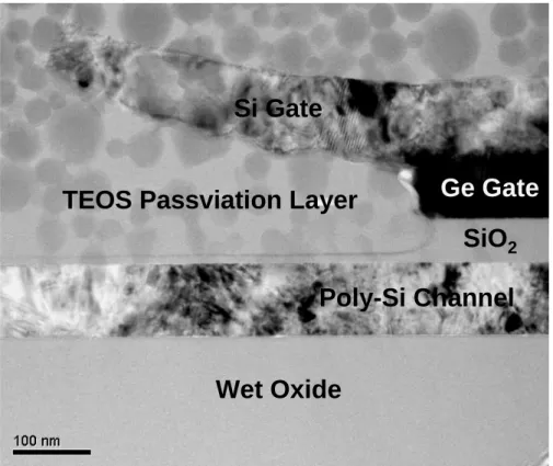
In order to demonstrate that the T- gate structure has been fabricated, and the length of the T-gate undercut region, weuse the transmission electron microscope (TEM) and scanning electron microscopy (SEM) to confirm.
Fig.2.1 The schematic cross section of the Si/Ge T-Gate TFTs with TEOS passivation
Fig.2.2 The schematic cross section of the Si/Ge T-Gate TFTs with Si3N4 passivation
Fig.2.3 The schematic cross section of conventional TFTs
TEOS
Poly-Si
n
+Si
Buried oxide
n+ n+TEOS
Al Al AlTEOS
TEOS
TEOS
Poly-Si
n
+Si
Buried oxide
n
+Ge
n
+n
+TEOS
Al Al Al Si3N4 Si3N4TEOS
Poly-Si
n
+Si
Buried oxide
n
+Ge
n+ n+TEOS
Al Al Al TEOS TEOS(1) 550 nm thick buried oxide and 50/100nm thick a-Si were deposited.
(2) 600°C annealing for 24-hr and active region definition.
(3) 50 nm thick TEOS oxide was deposited.
(4) 50/100nm thick germanium layer and 150/100nm thick a-Si were deposited.
Buried oxide
Poly-Si
TEOS
Buried oxide
Poly-Si
Buried oxide
a-Si
a-Si
Buried oxide
Poly-Si
TEOS
Ge
(5) Phosphorous implantation.
(6) Gate definition.
(7) Si/Ge T-Gate structure formation.
a-Si
Buried oxide
Poly-Si
TEOS
Ge
Implant
a-Si
Buried oxide
Poly-Si
TEOS
Ge
a-Si
Buried oxide
TEOS
Ge
Poly-Si
(8) Source/Drain region formation.
(9) TEOS passivation layer.
(10) Contact hole and metal pad.
Fig. 2.1 Process flows of Si/Ge T-Gate TFTs.
Implant
n
+a-Si
Buried oxide
Poly-Si
Ge
n
+n
+TEOS
n
+TEOS
Poly-Si
n
+Si
Buried oxide
n
+Ge
n
+n
+TEOS
TEOS PassivationTEOS
Poly-Si
n
+Si
Buried oxide
n
+Ge
n
+n
+TEOS
Al Al Al TEOS TEOSTable 3.1 Split condition for all samples with different thickness of stacked
Si/Ge and undercut length.
Device Channel thickness
Gate oxide
Gate (Si/ Ge) Undercut
Si/Ge50nm T-gate TFT(400nm) 400nm Si/Ge50nm T-gate TFT(800nm) 150nm / 50nm 800nm Si/Ge50nm T-gate TFT(400nm) 400nm Si/Ge50nm T-gate TFT(800nm) 50nm 100nm / 100nm 800nm Si/Ge100nm T-gate TFT(400nm) 400nm Si/Ge100nm T-gate TFT(800nm) 150nm / 50nm 800nm Si/Ge100nm T-gate TFT(400nm) 400nm Si/Ge100nm T-gate TFT(800nm) 100nm All 50nm 100nm / 100nm 800nm
Table 3.2 Split conditions for control devices.
Device Channel thickness
Gate oxide
Gate (a-Si film) Undercut
Conventional TFT 50nm 200nm
Conventional TFT 100nm
50nm
Chapter 3
Electrical Characterization of the Si/Ge T-gate TFTs
At first, the cross-section TEM of T-gate TFTs is shown in Fig.3.1. Thickness of channel film, gate oxide, gate, and undercut length are shown in Fig.3.2. Fig. 3.3 shows the SEM image of the Stacked Si/Ge gate with undercut structure. The T-Gate structure was successfully fabricated, which had shown in the TEM and SEM pictures clearly. In this chapter, the electrical characteristics of the Si/Ge T-gate TFTs and conventional TFTs are discussed carefully. The device parameters including threshold voltage (VTH), subthreshold
swing (S.S.), On current (ION), Off current (IOFF), and On/Off current ratio are all extracted. In
order to verify the effect of the T-Gate structure on the vertical and lateral electric field near the drain, the electric field in the TFT was simulated by employing the commercial 2-D simulator for semiconductor device.
3.1 Device Simulation
As we know that the undesirable effect, anomalous leakage current, kink effect, and hot-carrier effect, are related to the lateral electric field in the channel. In order to study the electric field effects of the various LTPS TFT structures, the two-dimensional (2D) numerical device simulator TCAD- ISE (Integrated Systems Engineering) was utilized.
The 2D cross-section of TFTs structure obtained from DIOS-ISE process simulation. The device simulation grids for the structures are generated using MDRAW-ISE. For electrical analysis is then carrier out in DESSIS-ISE on the structures. We consider the drift-diffusion model in our calculation.
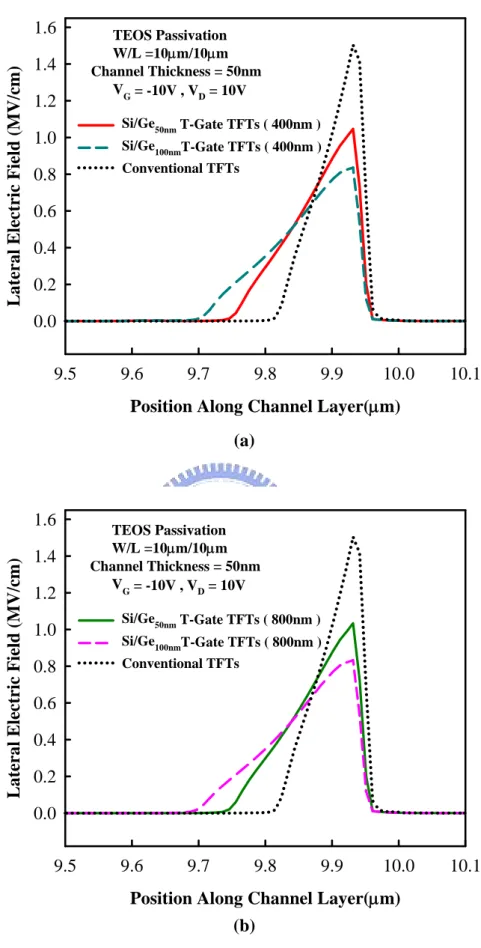
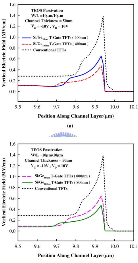
interface for VG= -10V and VD= 10V. At the active layer surface under the T-Gate structure,
the vertical electric field and lateral electric field are reduced considerably compared with conventional TFT. Especially, the Si/Ge T-Gate TFTs with high thickness of the germanium layer have shown a lower electric field than that of the Si/Ge T-Gate TFTs with 400nm germanium layer thickness.
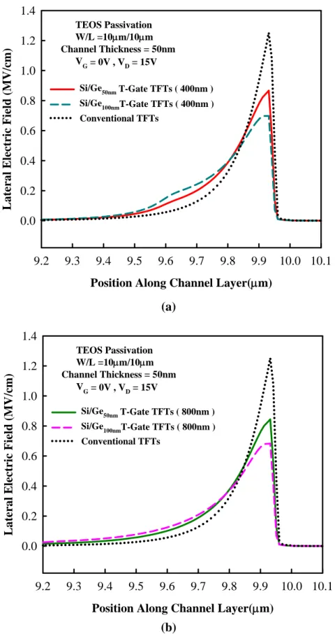
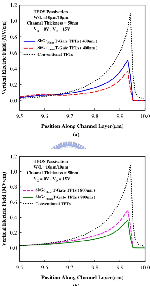
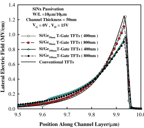
Fig.3.6 and Fig.3.7 show the electric field distribution along the channel/gate insulator interface for VG= 0V and VD= 15V. It is also found that the Si/Ge T-Gate TFTs with TEOS
passivation reduce both horizontal and vertical electric fields.
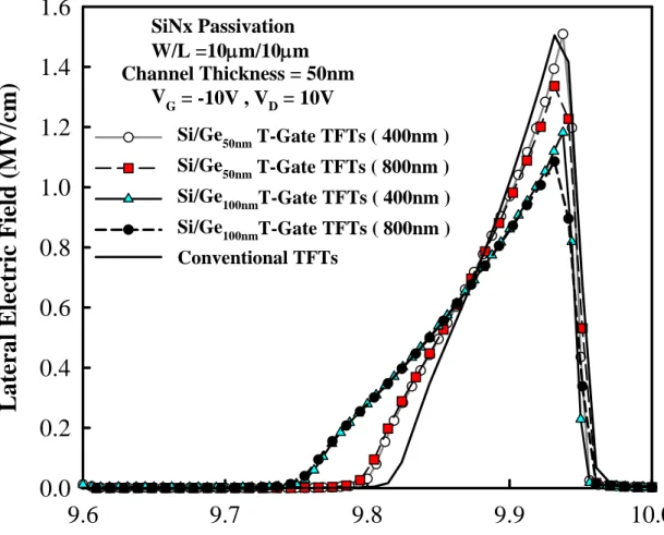
Fig. 3.8 and Fig.3.9 show the simulated electric field distribution for Si/Ge T-Gate TFTs with Si3N4 passivation. Results show that higher electric field at the drain edge of the
high-k passivation TFT compared to the TEOS passivation TFT. The vertical and lateral electric field distribution along the channel/gate insulator interface for VG= 0V and VD= 15V
are shown in Fig.3.10 and Fig.3.11.
It is well known that the leakage current increases significantly with the increase of gate voltage and drain voltage due to the field enhanced generation [32][33]. The lateral peak electric field in the depletion region between the p+ accumulation layer and the n+ drain causes the field emission via trap states, which makes the leakage current increase with drain voltage. Increase of gate voltage increases the vertical electric field around the interface between the gate oxide and the active poly-Si near the drain, which causes the serious increase of leakage current due to the enhanced thermal generation [34].
3.2 Basic Electrical Characteristics of Si/Ge T-Gate TFTs
3.2.1 Transfer Characteristics
The ID-VG characteristics of an n-channel Si/Ge T-Gate TFTs with different gate length
(10μm、8μm、5μm、3μm) are shown in Fig.3.12~Fig.3.15. The leakage current of the Si/Ge T-Gate TFTs is lower bytwo orders of magnitudethan that of conventional devices at
VG = -10V. It is because that T-Gate TFTs could effectively reduce the electric field near the
drain junction. For an LPCVD polysilicon TFT, according to the trap-assisted field-emission model, the leakage current can be expressed as [32]
1 D L e T TC TV y V I qZx N E τ τ ⎛ ⎞ ⎛ ⎞ ≈ ⎜ ⎟⎜⎜ ⎟⎟ + ⎝ ⎠⎝ ⎠ (Eq.2)
wherex is the effective depth of the junction region, Z is the channel width, and Ne T is the trap
density. The time constantsτTCandτTVrepresent the probability per unit time that a trapped carrier will tunnel through a triangular barrier at the channel/drain junction, which is exponentially dependent on the inverse of the strength of the lateral electric field Ey.
Therefore, the leakage current can be reduced by decreasing the electric field at the channel/drain junction region.
The off-state current of the Si/Ge T-Gate TFTs are much lower than that of the conventional TFT. When the germanium layer thickness is increased, the off-state leakage current is reduced at VD = 10V, compared to the conventional TFT, which is due to the
vertical electric field and lateral electric field near the drain edge are both reduced. As channel length is reduced, the leakage current is lower with increase of the T-Gate height is obviously.
Fig.3.16~Fig.3.19 show the transfer characteristics of the Si/Ge T-Gate TFTs with high channel thickness (100nm), the leakage current are also reduced significantly with increase of germanium layer thickness and undercut length.
The off-state leakage current was effectively suppressed in the Si/Ge T-Gate TFTs with channel thickness 50nm, especially when the increase of germanium layer thickness and undercut length. However, the on-current for these conditions is decreased due to the increased series resistance caused by the undercut regions. Hence, the Si3N4 with higher
dielectric constant was used to improve the on-state characteristic.
The ID-VG characteristics of the Si/Ge T-Gate TFTs with a Si3N4 passivation for
TFTs have better subthreshold swing and high Ion than those TFTs with a TEOS passivation.
High dielectric constant materials have been used to increase capacitance Cox which could
improve the on-state current. The combination of T-Gate structure and Si3N4 material can
suppress the electric field and improve the on-state characteristics.
3.2.2 On/Off Current Ratio
Fig.3.24 show the gate length dependence of On/Off current ratio in Si/Ge T-gate TFTs with TEOS passivation and conventional TFT. The devices with 50/ 100nm thickness of channel film are shown in the figure (a) and (b). The higher series resistance of the undercut regions slightly degrades the on-current of the Si/Ge T-Gate TFTs with thick germanium film. For this reason, the On/Off current ratio is lower than the thin germanium film devices, as shown in figure (a).
For the channel thickness is increased, shown in Fig.3.24 (b), the influence of series resistance is slightly released when increasing the thickness of germanium layer. In addition, the off-state leakage current of the Si/Ge T-Gate TFTs with thick germanium film is lower than other devices. TheSi/Ge T-Gate TFTs with 100nm thickness of germanium layer have increased the On/Off current ratio relative to the Si/Ge T-Gate TFTs with 50nm thickness of germanium film.
The Si/Ge T-Gate TFTs with a Si3N4 passivation was shown in Figure 3.25. The
On/Off current ratio trend is similar in the T-Gate devices because of the on-state current is considerably increased and off-state leakage current is almostthe same.
All conventional TFTs show a smaller On/ Off current ratio among these devices, which is due to the leakage current can not be effectively suppressed with large electric field near the drain edge.
3.2.3 Off-State Leakage
The temperature dependence of the mobile holes in equilibrium with the trapped charge is given by [35] 0 a E kT off
I
=
I e
− (Eq.3)I0 = constant independent of temperature, and Ea = drain current activation energy which
measures the difference between the valence band edge and the energy of the grain boundary states within kT of the Fermi level. In TFTs, the increase in the electric field strength causes the decrease of the leakage current activation energy [36]. As the drain bias increases, the drain depletion field increases and Ea decreases. This suggest that the high electric field in the
drain depletion region has reduced the barrier that carrier must overcome. This leakage current mechanism is thermionic field emission[35].
The Off-state leakage current characteristics are shown in Fig.3.26 and Fig.3.27. The Si/Ge T-Gate TFTs show the leakage current as low as 1pA/μm. It is because the T-Gate structure can effectively suppress the electric field near the drain edge. In the conventional TFT, Ioff abruptly increases with increasing Vd because of the thermionic field emission
current at drain junction [37].
3.2.4 Output Characteristics
The current increase in the output characteristics at large VDS, usually referred to as
“kink effect,” is explained by impact ionization occurring in the high-field region at the drain end of the channel. Its effect is enhanced by the action of a parasitic bipolar transistor in the back-channel region, whose base current arises from the impact generated holes[38].
Figure 3.28~ Figure 3.30 show the output characteristics of conventional TFTs and Si/Ge T-gate TFTs with W/L=10μm/10μm. The ID-VD performances of the Si/Ge T-gate TFTs
effect at high drain biases is a result of the exaggerated avalanche multiplication near drain junction caused by the high drain field and large amount of traps [39].
Impact ionization has been modeled by the Chynoweth expressions of the ionization rates for electrons (αn) and holes (αp) [40]
exp n n an b F α = ⎛⎜− ⎞⎟ ⎝ ⎠ exp p p p b a F α = ⎛⎜− ⎞⎟ ⎝ ⎠ (Eq.4)
where F∥ is the component of the electric field along the current-flow direction. The
ionization rate is reduced by suppressing lateral electric field. Therefore, at very high source-drain voltages, drain avalanche is unobvious for T-Gate structure.
Figure 3.28 shows the result for (a) germanium layer thickness is 50nm, and (b) germanium layer thickness is 100nm. The device with thickness of germanium layer 100nm exhibits a smaller on-current than that of 50nm germanium layer case. This is because the series resistance is increased under the undercut region. However, floating body effect is reduced in Si/Ge T-gate TFTs with thick thickness of germanium film which caused by suppressed lateral electric field.
The kink effect in SOI MOSFETs is a combination of the channel avalanche multiplication occurred in the high-field region near the drain and the floating body effect at the channel of the device [41]. However, in poly-Si TFTs, there is an additional mechanism that causes the poor saturation characteristics. It is the high grain-boundary trap density in the poly-Si material that exaggerates the effect of the avalanche multiplication [42] [43].
When channel film is increased, the grain-boundary trap density in the channel will cause the sever kink effect at high drain biases, as shown in Figure 3.29. But it is found that the Si/Ge T-gate TFTs exhibits with good current saturation characteristics compared with conventional TFT. In the conventional TFT, the higher lateral electric field will generate more hot carriers which cause seriously floating body effect to occur.
in the Fig.3.30. The anomalous current was suppressed at VD< 15V and the on-current
characteristic are better than those TFT with a TEOS passivation. But the drain avalanche occurs as the drain voltage is increased, which is due to the lateral electric field is larger than the Si/Ge T-Gate TFTs with a TEOS passivation. In order to obtain excellent saturation characteristics in the low temperature poly-Si (LTPS) TFT’s, both the high electric field and high grain-boundary trap density at the channel near the drain must to be reduced effectively.
3.2.5 Hot Carrier Stress
Hot carrier stress was used to test the long-term reliability of LTPS TFT in this work. Hot carrier instabilities in poly-Si thin film transistors are caused by high electric fields at the drain. These high fields are determined mainly by the abruptness of the lateral n+ doping profile in the drain and the two-dimensional (2D) coupling of the x and y components of the electric field between the gate and drain [44]. Fig.3.31 illustrating the time evolution (0 < t < 103) of the relative on-current degradation that bias-stressing at VGS = 10V, VDS = 20V cause
minor Δ for the Si/Ge T-gate TFTs which compared with conventional TFTs. The trend Ion of Si/Ge T-gate TFTs with different conditions were shown in these figures. The device with the 100nm-thick of germanium layer shows larger on-current degradation than that of 50nm case. This is because the increased series resistance under the undercut region causing a reduced I×R drop and on-state current. However, the Si/Ge T-gate TFTs still have lower Ion
variation than the conventional TFTs, since thelateral electric field is reduced.
Figure 3.32 (a)~(b) show the ∆VTH versus stress time for conventional TFTs and Si/Ge
T-gate TFTs with different channel length ( W/L=10μm/10μm, 5μm). These figures illustrate the threshold voltage variations and the degradation in a poly-Si TFTs under static hot-carrier stress and the DC stress conditions are VDS = 10V and VGS = 20V for 1000s. The
large drain junction electric field under hot carrier stress resulted in serious degradation on conventional TFTs, was due to the high electric field at the drain junction. The high electric
field promotes impact ionization, resulting in numerous grain-boundary traps being created in the drain junction. On the other hand, the Si/Ge T-gate TFTs exhibited better hot carrier endurance than conventional one resulted from the relief of drain junction electric field.
Fig. 3.1 Stacked Si/Ge gate with the germanium undercut structure observed by cross section TEM microphotographs.
Fig. 3.2 Thickness of channel film, gate oxide, gate, and undercut length are shown in this picture.
Ge Gate
Si Gate
SiO
2Poly-Si Channel
TEOS Passviation Layer
Wet Oxide
Ge Gate
Si Gate
SiO
2Poly-Si Channel
TEOS Passviation Layer
(a)
(b)
Fig. 3.4 The simulated lateral electric field along the channel (10μm) direction near the drain the VG= -10V, VD= 10V. The different stacked Si/Ge gate thichness with TEOS passivation of
(a) Undercut length is 400nm. (b) Undercut length is 800nm.
TEOS Passivation
W/L =10μm/10μm
Channel Thickness = 50nm
VG = -10V , VD = 10V
Position Along Channel Layer(μm)
9.5 9.6 9.7 9.8 9.9 10.0 10.1
Lateral Electric Field (MV/cm)
0.0 0.2 0.4 0.6 0.8 1.0 1.2 1.4 1.6 Si/Ge50nm T-Gate TFTs ( 400nm ) Si/Ge100nmT-Gate TFTs ( 400nm ) Conventional TFTs TEOS Passivation W/L =10μm/10μm Channel Thickness = 50nm VG = -10V , VD = 10V
Position Along Channel Layer(μm)
9.5 9.6 9.7 9.8 9.9 10.0 10.1
Lateral Electric Field (MV/cm)
0.0 0.2 0.4 0.6 0.8 1.0 1.2 1.4 1.6 Si/Ge50nm T-Gate TFTs ( 800nm ) Si/Ge100nmT-Gate TFTs ( 800nm ) Conventional TFTs
(a)
(a)
(b)
Fig. 3.5 The simulated vertical electric field along the channel (10μm) direction near the drain the VG= -10V, VD= 10V. The different stacked Si/Ge gate thichness with TEOS
passivation of (a) undercut length is 400nm. (b) undercut length is 800nm.
TEOS Passivation
W/L =10μm/10μm
Channel Thickness = 50nm
VG = -10V , VD = 10V
Position Along Channel Layer(μm)
9.5 9.6 9.7 9.8 9.9 10.0 10.1 Ver ti ca l El ec tri c Fi eld (MV/ cm ) 0.0 0.2 0.4 0.6 0.8 1.0 1.2 1.4 1.6 Si/Ge50nm T-Gate TFTs ( 400nm ) Si/Ge100nmT-Gate TFTs ( 400nm ) Conventional TFTs TEOS Passivation W/L =10μm/10μm Channel Thickness = 50nm VG = -10V , VD = 10V
Position Along Channel Layer(μm)
9.5 9.6 9.7 9.8 9.9 10.0 10.1 Ver ti ca l El ec tri c Fi eld (MV/ cm ) 0.0 0.2 0.4 0.6 0.8 1.0 1.2 1.4 1.6 Si/Ge 50nm T-Gate TFTs ( 800nm ) Si/Ge100nmT-Gate TFTs ( 800nm ) Conventional TFTs
(a)
(b)
Fig. 3.6 The simulated lateral electric field along the channel (10μm) direction near the drain the VG= 0V, VD= 15V. The different stacked Si/Ge gate thichness with TEOS passivation of
(a) undercut length is 400nm. (b) undercut length is 800nm.
TEOS Passivation
W/L =10μm/10μm
Channel Thickness = 50nm
VG = 0V , VD = 15V
Position Along Channel Layer(μm)
9.2 9.3 9.4 9.5 9.6 9.7 9.8 9.9 10.0 10.1 Late ral Ele ctric Field (MV/cm) 0.0 0.2 0.4 0.6 0.8 1.0 1.2 1.4 Si/Ge 50nm T-Gate TFTs ( 800nm ) Si/Ge100nmT-Gate TFTs ( 800nm ) Conventional TFTs TEOS Passivation W/L =10μm/10μm Channel Thickness = 50nm VG = 0V , VD = 15V
Position Along Channel Layer(μm)
9.2 9.3 9.4 9.5 9.6 9.7 9.8 9.9 10.0 10.1 Late ral Ele ctric Field (MV/cm) 0.0 0.2 0.4 0.6 0.8 1.0 1.2 1.4 Si/Ge50nm T-Gate TFTs ( 400nm ) Si/Ge100nmT-Gate TFTs ( 400nm ) Conventional TFTs
(a)
(b)
Fig. 3.7 The simulated vertical electric field along the channel (10μm) direction near the drain the VG= 0V, VD= 15V. The different stacked Si/Ge gate thichness with TEOS
passivation of (a) undercut length is 400nm. (b) undercut length is 800nm.
TEOS Passivation
W/L =10μm/10μm
Channel Thickness = 50nm
VG = 0V , VD = 15V
Position Along Channel Layer(μm)
9.5 9.6 9.7 9.8 9.9 10.0 Vert ic a l El ect ric Fiel d (M V/ cm ) 0.0 0.2 0.4 0.6 0.8 1.0 1.2 Si/Ge50nm T-Gate TFTs ( 400nm ) Si/Ge 100nmT-Gate TFTs ( 400nm ) Conventional TFTs TEOS Passivation W/L =10μm/10μm Channel Thickness = 50nm VG = 0V , VD = 15V
Position Along Channel Layer(μm)
9.5 9.6 9.7 9.8 9.9 10.0 Vert ic a l El ect ric Fiel d (M V/ cm ) 0.0 0.2 0.4 0.6 0.8 1.0 1.2 Si/Ge50nm T-Gate TFTs ( 800nm ) Si/Ge100nmT-Gate TFTs ( 800nm ) Conventional TFTs
Fig. 3.8 The simulated lateral electric field along the channel (10μm) direction near the drain the VG= -10V, VD= 10V. The different stacked Si/Ge gate thichness with SiNx
passivation are shown.
SiNx Passivation W/L =10μm/10μm Channel Thickness = 50nm VG = -10V , VD = 10V
Position Along Channel Layer(
μm)
9.6
9.7
9.8
9.9
10.0
Lateral Electric Field
(MV/cm)
0.0
0.2
0.4
0.6
0.8
1.0
1.2
1.4
1.6
Si/Ge50nm T-Gate TFTs ( 400nm ) Si/Ge50nm T-Gate TFTs ( 800nm ) Si/Ge100nmT-Gate TFTs ( 400nm ) Si/Ge100nmT-Gate TFTs ( 800nm ) Conventional TFTsFig. 3.9 The simulated vertical electric field along the channel (10μm) direction near the drain the VG= -10V, VD= 10V. The different stacked Si/Ge gate thichness with SiNx
passivation are shown.
SiNx Passivation W/L =10μm/10μm Channel Thickness = 50nm VG = -10V , VD = 10V
Position Along Channel Layer(
μm)
9.6
9.7
9.8
9.9
10.0
Vertical Electric Field
(MV/cm)
0.0
0.2
0.4
0.6
0.8
1.0
1.2
1.4
1.6
Si/Ge50nm T-Gate TFTs ( 400nm ) Si/Ge50nm T-Gate TFTs ( 800nm ) Si/Ge100nmT-Gate TFTs ( 400nm ) Si/Ge100nmT-Gate TFTs ( 800nm ) Conventional TFTsFig. 3.10 The simulated lateral electric field along the channel (10μm) direction near the drain the VG= 0V, VD= 15V. The different stacked Si/Ge gate thichness with SiNx
passivation are shown.
SiNx Passivation W/L =10μm/10μm Channel Thickness = 50nm VG = 0V , VD = 15V
Position Along Channel Layer(
μm)
9.5
9.6
9.7
9.8
9.9
10.0
Lateral Electric Field
(MV/cm)
0.0
0.2
0.4
0.6
0.8
1.0
1.2
1.4
Si/Ge50nm T-Gate TFTs ( 400nm ) Si/Ge50nm T-Gate TFTs ( 800nm ) Si/Ge100nmT-Gate TFTs ( 400nm ) Si/Ge100nmT-Gate TFTs ( 800nm ) Conventional TFTsFig. 3.11 The simulated vertical electric field along the channel (10μm) direction near the drain the VG= 0V, VD= 15V. The different stacked Si/Ge gate thichness with SiNx
passivation are shown.
SiNx Passivation W/L =10μm/10μm Channel Thickness = 50nm VG = 0V , VD = 15V
Position Along Channel Layer(
μm)
9.6
9.7
9.8
9.9
10.0
Vertical Electric Field (MV/cm)
0.0
0.2
0.4
0.6
0.8
1.0
1.2
1.4
Si/Ge50nm T-Gate TFTs ( 400nm ) Si/Ge50nm T-Gate TFTs ( 800nm ) Si/Ge100nmT-Gate TFTs ( 400nm ) Si/Ge100nmT-Gate TFTs ( 800nm ) Conventional TFTs(a) (b) TEOS Passivation W/L = 10μm/ 10μm Channel Thickness = 50nm VD= 10.0V Gate Voltage VG ( V ) -10 -5 0 5 10 15 20 D rain Curr ent I ( A D ) 10-12 10-11 10-10 10-9 10-8 10-7 10-6 10-5 10-4 10-3 Si / Ge 100nmT-Gate TFTs ( 400nm ) Si / Ge 100nmT-Gate TFTs ( 800nm ) Conventional TFTs TEOS Passivation W/L = 10μm/ 10μm Channel Thickness = 50nm VD= 10.0V Gate Voltage VG ( V ) -10 -5 0 5 10 15 20 D rain Curr ent I ( A D ) 10-12 10-11 10-10 10-9 10-8 10-7 10-6 10-5 10-4 10-3 Si / Ge 50nm T-Gate TFTs ( 400nm ) Si / Ge 50nm T-Gate TFTs ( 800nm ) Conventional TFTs
(c)
(d)
Fig.3.12(a) ~ (d)The transfer characteristics of the Si/Ge T-Gate TFTs with different thickness of stacked Si/Ge and undercut length. The channel thickness is 50nm and gate length is 5μm.
TEOS Passivation W/L = 10μm/ 10μm Channel Thickness = 50nm VD= 10.0V Gate Voltage VG ( V ) -10 -5 0 5 10 15 20 Drain Current I ( AD ) 10-12 10-11 10-10 10-9 10-8 10-7 10-6 10-5 10-4 10-3 Si / Ge 50nm T-Gate TFTs ( 400nm ) Si / Ge 100nmT-Gate TFTs ( 400nm ) Conventional TFTs TEOS Passivation W/L = 10μm/ 10μm Channel Thickness = 50nm VD= 10.0V Gate Voltage VG ( V ) -10 -5 0 5 10 15 20 D rain Curr ent I ( A D ) 10-12 10-11 10-10 10-9 10-8 10-7 10-6 10-5 10-4 10-3 Si / Ge 50nmT-Gate TFTs ( 800nm ) Si / Ge 100nmT-Gate TFTs ( 800nm ) Conventional TFTs
(a) (b) TEOS Passivation W/L = 10μm/ 8μm Channel Thickness = 50nm VD= 10.0V Gate Voltage VG ( V ) -10 -5 0 5 10 15 20 Drain Current I ( AD ) 10-12 10-11 10-10 10-9 10-8 10-7 10-6 10-5 10-4 10-3 Si / Ge 50nm T-Gate TFTs ( 400nm ) Si / Ge 50nm T-Gate TFTs ( 800nm ) Conventional TFTs TEOS Passivation W/L = 10μm/ 8μm Channel Thickness = 50nm VD= 10.0V Gate Voltage VG ( V ) -10 -5 0 5 10 15 20 D rain Curr ent I ( A D ) 10-12 10-11 10-10 10-9 10-8 10-7 10-6 10-5 10-4 10-3 Si / Ge 100nmT-Gate TFTs ( 400nm ) Si / Ge 100nmT-Gate TFTs ( 800nm ) Conventional TFTs
(c)
(d)
Fig.3.13(a) ~ (d)The transfer characteristics of the Si/Ge T-Gate TFTs with different thickness of stacked Si/Ge and undercut length. The channel thickness is 50nm and gate length is 8μm.
TEOS Passivation W/L = 10μm/ 8μm Channel Thickness = 50nm VD= 10.0V Gate Voltage VG ( V ) -10 -5 0 5 10 15 20 Drain Current I ( AD ) 10-12 10-11 10-10 10-9 10-8 10-7 10-6 10-5 10-4 10-3 Si / Ge 50nm T-Gate TFTs ( 400nm ) Si / Ge 100nmT-Gate TFTs ( 400nm ) Conventional TFTs TEOS Passivation W/L = 10μm/ 8μm Channel Thickness = 50nm VD= 10.0V Gate Voltage VG ( V ) -10 -5 0 5 10 15 20 Drain Current I ( AD ) 10-12 10-11 10-10 10-9 10-8 10-7 10-6 10-5 10-4 10-3 Si / Ge 50nm T-Gate TFTs ( 800nm ) Si / Ge 100nmT-Gate TFTs ( 800nm ) Conventional TFTs
(a) (b) TEOS Passivation W/L = 10μm/ 5μm Channel Thickness = 50nm VD= 10.0V Gate Voltage VG ( V ) -10 -5 0 5 10 15 20 Drain Current I ( AD ) 10-12 10-11 10-10 10-9 10-8 10-7 10-6 10-5 10-4 10-3 10-2 Si / Ge 50nm T-Gate TFTs ( 400nm ) Si / Ge 50nm T-Gate TFTs ( 800nm ) Conventional TFTs TEOS Passivation W/L = 10μm/ 5μm Channel Thickness = 50nm VD= 10.0V Gate Voltage VG ( V ) -10 -5 0 5 10 15 20 D rain Curr ent I ( A D ) 10-12 10-11 10-10 10-9 10-8 10-7 10-6 10-5 10-4 10-3 10-2 Si / Ge 100nm T-Gate TFTs ( 400nm ) Si / Ge 100nm T-Gate TFTs ( 800nm ) Conventional TFTs
(c)
(d)
Fig.3.14(a) ~ (d)The transfer characteristics of the Si/Ge T-Gate TFTs with different thickness of stacked Si/Ge and undercut length. The channel thickness is 50nm and gate length is 5μm.
TEOS Passivation W/L = 10μm/ 5μm Channel Thickness = 50nm VD= 10.0V Gate Voltage VG ( V ) -10 -5 0 5 10 15 20 Drain Current I ( AD ) 10-12 10-11 10-10 10-9 10-8 10-7 10-6 10-5 10-4 10-3 10-2 Si / Ge 50nm T-Gate TFTs ( 400nm ) Si / Ge 100nmT-Gate TFTs ( 400nm ) Conventional TFTs TEOS Passivation W/L = 10μm/ 5μm Channel Thickness = 50nm VD= 10.0V Gate Voltage VG ( V ) -10 -5 0 5 10 15 20 D rain Curr ent I ( A D ) 10-12 10-11 10-10 10-9 10-8 10-7 10-6 10-5 10-4 10-3 10-2 Si / Ge 50nmT-Gate TFTs ( 800nm ) Si / Ge 100nmT-Gate TFTs ( 800nm ) Conventional TFTs
(a) (b) TEOS Passivation W/L = 10μm/ 3μm Channel Thickness = 50nm VD= 10.0V Gate Voltage VG ( V ) -10 -5 0 5 10 15 20 D rain Curr ent I ( A D ) 10-12 10-11 10-10 10-9 10-8 10-7 10-6 10-5 10-4 10-3 10-2 Si / Ge 50nm T-Gate TFTs ( 400nm ) Si / Ge 50nm T-Gate TFTs ( 800nm ) Conventional TFTs TEOS Passivation W/L = 10μm/ 3μm Channel Thickness = 50nm VD= 10.0V Gate Voltage VG ( V ) -10 -5 0 5 10 15 20 D rain Curr ent I ( A D ) 10-12 10-11 10-10 10-9 10-8 10-7 10-6 10-5 10-4 10-3 10-2 Si / Ge 100nm T-Gate TFTs ( 400nm ) Si / Ge 100nm T-Gate TFTs ( 800nm ) Conventional TFTs
(c)
(d)
Fig.3.15(a) ~ (d)The transfer characteristics of the Si/Ge T-Gate TFTs with different thickness of stacked Si/Ge and undercut length. The channel thickness is 50nm and gate length is 3μm.
TEOS Passivation W/L = 10μm/ 3μm Channel Thickness = 50nm VD= 10.0V Gate Voltage VG ( V ) -10 -5 0 5 10 15 20 D rain Curr ent I ( A D ) 10-12 10-11 10-10 10-9 10-8 10-7 10-6 10-5 10-4 10-3 10-2 Si / Ge 50nm T-Gate TFTs ( 400nm ) Si / Ge 100nmT-Gate TFTs ( 400nm ) Conventional TFTs TEOS Passivation W/L = 10μm/ 3μm Channel Thickness = 50nm VD= 10.0V Gate Voltage VG ( V ) -10 -5 0 5 10 15 20 D rain Curr ent I ( A D ) 10-12 10-11 10-10 10-9 10-8 10-7 10-6 10-5 10-4 10-3 10-2 Si / Ge 50nm T-Gate TFTs ( 800nm ) Si / Ge 100nmT-Gate TFTs ( 800nm ) Conventional TFTs
Fig.3.16 The transfer characteristics of the Si/Ge T-Gate TFTs with different thickness of stacked Si/Ge and undercut length. The channel thickness is 100nm and gate length is 10μm.
TEOS Passivation W/L = 10μm/10μm Channel Thickness = 100nm VD= 10.0V Gate Voltage VG ( V ) -10 -5 0 5 10 15 20 Drain Current I D ( A ) 10-12 10-11 10-10 10-9 10-8 10-7 10-6 10-5 10-4 10-3 Si / Ge 50nmT-Gate TFTs ( 400nm ) Si / Ge 50nmT-Gate TFTs ( 800nm ) Si / Ge 100nmT-Gate TFTs ( 400nm ) Si / Ge 100nmT-Gate TFTs ( 800nm ) Conventional TFTs
Fig.3.17 The transfer characteristics of the Si/Ge T-Gate TFTs with different thickness of stacked Si/Ge and undercut length. The channel thickness is 100nm and gate length is 8μm.
TEOS Passivation W/L = 10μm/ 8μm Channel Thickness = 100nm VD= 10.0V Gate Voltage VG ( V ) -10 -5 0 5 10 15 20 Drain Current I D ( A ) 10-12 10-11 10-10 10-9 10-8 10-7 10-6 10-5 10-4 10-3 10-2 Si / Ge 50nmT-Gate TFTs ( 400nm ) Si / Ge 50nmT-Gate TFTs ( 800nm ) Si / Ge 100nmT-Gate TFTs ( 400nm ) Si / Ge 100nmT-Gate TFTs ( 800nm ) Conventional TFTs
Fig.3.18 The transfer characteristics of the Si/Ge T-Gate TFTs with different thickness of stacked Si/Ge and undercut length. The channel thickness is 100nm and gate length is 5μm.
TEOS Passivation W/L = 10μm/ 5μm Channel Thickness = 100nm VD= 10.0V Gate Voltage VG ( V ) -10 -5 0 5 10 15 20 Drain Current I D ( A ) 10-12 10-11 10-10 10-9 10-8 10-7 10-6 10-5 10-4 10-3 10-2 Si / Ge 50nmT-Gate TFTs ( 400nm ) Si / Ge 50nmT-Gate TFTs ( 800nm ) Si / Ge 100nmT-Gate TFTs ( 400nm ) Si / Ge 100nmT-Gate TFTs ( 800nm ) Conventional TFTs
Fig.3.19 The transfer characteristics of the Si/Ge T-Gate TFTs with different thickness of stacked Si/Ge and undercut length. The channel thickness is 100nm and gate length is 3μm.
TEOS Passivation W/L = 10μm/ 3μm Channel Thickness = 100nm VD= 10.0V Gate Voltage VG ( V ) -10 -5 0 5 10 15 20 Drain Current I D ( A ) 10-12 10-11 10-10 10-9 10-8 10-7 10-6 10-5 10-4 10-3 10-2 Si / Ge 50nmT-Gate TFTs ( 400nm ) Si / Ge 50nmT-Gate TFTs ( 800nm ) Si / Ge 100nmT-Gate TFTs ( 400nm ) Si / Ge 100nmT-Gate TFTs ( 800nm ) Conventional TFTs
(a) (b) SiNx Passivation W/L = 10μm/10μm Channel Thickness = 50nm VD= 10V Gate Voltage VG ( V ) -10 -5 0 5 10 15 20 Drain Current I D ( A ) 10-12 10-11 10-10 10-9 10-8 10-7 10-6 10-5 10-4 10-3 Si / Ge 50nmT-Gate TFTs ( 400nm ) Si / Ge 50nmT-Gate TFTs ( 800nm ) Conventional TFTs SiNx Passivation W/L = 10μm/10μm Channel Thickness = 50nm VD= 10V Gate Voltage VG ( V ) -10 -5 0 5 10 15 20 Drain Current I D ( A ) 10-12 10-11 10-10 10-9 10-8 10-7 10-6 10-5 10-4 10-3 Si / Ge 100nmT-Gate TFTs ( 400nm ) Si / Ge 100nmT-Gate TFTs ( 800nm ) Conventional TFTs
(c)
(d)
Fig.3.20(a) ~ (d)The transfer characteristics of the Si/Ge T-Gate TFTs with different thickness of stacked Si/Ge and undercut length. The channel thickness is 50nm, gate length is 10μm.
SiNx Passivation W/L = 10μm/10μm Channel Thickness = 50nm VD= 10V Gate Voltage VG ( V ) -10 -5 0 5 10 15 20 Drain Curr ent I D ( A ) 10-12 10-11 10-10 10-9 10-8 10-7 10-6 10-5 10-4 10-3 Si / Ge 50nmT-Gate TFTs ( 400nm ) Si / Ge 100nmT-Gate TFTs ( 400nm ) Conventional TFTs SiNx Passivation W/L = 10μm/10μm Channel Thickness = 50nm VD= 10V Gate Voltage VG ( V ) -10 -5 0 5 10 15 20 Drain Current I D ( A ) 10-12 10-11 10-10 10-9 10-8 10-7 10-6 10-5 10-4 10-3 Si / Ge 50nmT-Gate TFTs ( 800nm ) Si / Ge 100nmT-Gate TFTs ( 800nm ) Conventional TFTs
(a) (b) SiNx Passivation W/L = 10μm/8μm Channel Thickness = 50nm VD= 10V Gate Voltage VG ( V ) -10 -5 0 5 10 15 20 Drain Curr ent I D ( A ) 10-12 10-11 10-10 10-9 10-8 10-7 10-6 10-5 10-4 10-3 Si / Ge 50nmT-Gate TFTs ( 400nm ) Si / Ge 50nmT-Gate TFTs ( 800nm ) Conventional TFTs SiNx Passivation W/L = 10μm/8μm Channel Thickness = 50nm VD= 10V Gate Voltage VG ( V ) -10 -5 0 5 10 15 20 Drain Current I D ( A ) 10-12 10-11 10-10 10-9 10-8 10-7 10-6 10-5 10-4 10-3 Si / Ge 100nmT-Gate TFTs ( 400nm ) Si / Ge 100nmT-Gate TFTs ( 800nm ) Conventional TFTs
(c)
(d)
Fig.3.21(a) ~ (d)The transfer characteristics of the Si/Ge T-Gate TFTs with different thickness of stacked Si/Ge and undercut length. The channel thickness is 50nm, gate length is 8μm.
SiNx Passivation W/L = 10μm/8μm Channel Thickness = 50nm VD= 10V Gate Voltage VG ( V ) -10 -5 0 5 10 15 20 Drain Curr ent I D ( A ) 10-12 10-11 10-10 10-9 10-8 10-7 10-6 10-5 10-4 10-3 Si / Ge 50nmT-Gate TFTs ( 400nm ) Si / Ge 100nmT-Gate TFTs ( 400nm ) Conventional TFTs SiNx Passivation W/L = 10μm/8μm Channel Thickness = 50nm VD= 10V Gate Voltage VG ( V ) -10 -5 0 5 10 15 20 Drain Current I D ( A ) 10-12 10-11 10-10 10-9 10-8 10-7 10-6 10-5 10-4 10-3 Si / Ge 50nmT-Gate TFTs ( 800nm ) Si / Ge 100nmT-Gate TFTs ( 800nm ) Conventional TFTs