國
立
交
通
大
學
資訊科學與工程研究所
碩
士
論
文
管線化非同步 PIC18 微控制器之實作
A Novel Asynchronous Implementation of Pipelined
PIC18 Microcontroller
研 究 生:巫仁傑
指導教授:陳昌居 博士
管線化非同步 PIC18 微控制器之實作
ANovel Asynchronous Implementation of Pipelined PIC18
Microcontroller
研 究 生:巫仁傑 Student:Jen-Chieh Wu
指導教授:陳昌居 Advisor:Dr. Chang-Jiu Chen
國 立 交 通 大 學
資 訊 科 學 與 工 程 研 究 所
碩 士 論 文
A Thesis
Submitted to Institute of Computer Science and Engineering College of Computer Science
National Chiao Tung University in partial Fulfillment of the Requirements
for the Degree of Master
in
Computer Science June 2006
Hsinchu, Taiwan, Republic of China
中華民國九十五年七月
管線化非同步 PIC18 微控制器之實作
研究生:巫仁傑 指導教授:陳昌居 國立交通大學 資訊科學與工程學系摘要
非同步的電路設計可以很自然的解決同步電路設計的缺點,像是頻率歪斜,耗 電量,..等等的問題.但是目前使用非同步電路設計最大的問題就在於能使用的輔 助設計工具不夠多.PIC18 是由 Microchip 公司所開發出來的一系列 8 位元 RISC 架構的微控制 器.應用於許多嵌入式系統的設計.
我們的目標就是利用非同步電路的方式設計出與 PIC18 指令集相容的微處 理器. 同時也加入了管線的設計,以增加處理器的效能. 設計的工具我們選擇使 用 Verilog HDL. 最後我們模擬及驗證設計的正確性以效能.
A Novel Asynchronous Implementation of Pipelined
PIC18 Microcontroller
Student : Jen-Chieh Wu Advisor : Dr. Chang-Jiu Chen Department of Computer Science
National Chiao-Tung University
Abstract
Asynchronous design has a potential of solving some problems in synchronous design, such as clock skew and higher power consumption. However, the difficulty for asynchronous design is lack of CAD tools.
PIC18 is a serious of the 8-bit RISC architecture microcontroller developed by Microchip Technology Inc.. It is widely used in many embedded system designs.
Our goal is to design an asynchronous microprocessor compatible with PIC18 instruction sets. To increase the performance, the processor uses micropipeline design style. The design tool we choose is Verilog. Finally, the simulations show the correctness of the function and performance of its operation.
Acknowledgements
I would like to thank my advisor Prof. Chang-Jiu Chen for teaching me on my research, Prof. Fu-Chiung Cheng and his research group at Tatung University for their advices and contributions on the asynchronous PIC design. Also thanks to Mr. Wei-Ming Cheng for his careful proofreading of this thesis and my teammate Hung-Yue Tsai for discussing and co-working on this project. Thanks all the people who had ever helped me.
Contents
Abstract in Chinese……….…2 Abstract……….….…..3 Acknowledgements………..……4 Contents………..…..5 List of Figures………..……7 List of Tables………..…..9 Chapter 1: Introduction……….10 1.1 Overview………10 1.2 Motivations………...……….101.3 The Organization of This Thesis………11
Chapter 2: Background……….12 2.1 Synchronous Logic……….12 2.1.1 Synchronous Circuit………..…..12 2.1.2 Synchronous Pipeline………..12 2.2 Asynchronous Circuits………...…13 2.2.1 Handshake Protocols………...13
2.2.2 Classification of Asynchronous Circuits……….17
2.2.3 The Advantages of Asynchronous Circuits……….18
2.3 Asynchronous Pipeline………...19
2.3.1 C-element………....19
2.3.2 4-phase dual-rail Pipeline………20
Chapter 3: Asynchronous PIC18 Design………..23
3.1 Introduction of Microchip’s PIC18 microcontroller………..…23
3.1.2 Data Memory Map………..24
3.1.3 Instruction Set……….25
3.2 The Asynchronous PIC18 microprocessor architecture……….29
3.2.1 Instruction Set……….30
3.2.2 Construction of the Basic Elements………31
3.2.3 Pipeline Latch………..32
3.2.4 Design for each Stage………..33
3.2.5 Memory………...38
3.2.6 Register………39
3.2.7 Reset circuit……….40
3.3 Design flow………41
Chapter 4: Simulation Results………..42
4.1 Performance………...43
4.2 Cost………43
Chapter 5: Conclusions……….………45
List of Figures
Figure 2.1: Synchronous circuit………..11
Figure 2.2: Synchronous pipeline occupancy diagram……….12
Figure 2.3: Asynchronous handshake protocols………..13
Figure 2.4: Bundled Data channel (a); 4-phase bundled-data protocol (b); 2-phase bundled-data protocol (c)……….14
Figure 2.5: 4-phase dual-rail channel (a); 4-phase dual-rail protocol (b); 1-bit channel encoding chart………..15
Figure 2.6: C-element: (a) symbol; (b) possible implementation; (c) truth-table……19
Figure 2.7: A 3 stages (1-bit wide) pipeline………...20
Figure 2.8: (a) A 3-bit latch with completion detection; (b) Alternative completion detector……….20
Figure 2.9 Abstract view of data flow………..21
Figure 3.1: PIC18 microcontroller block diagram……...………23
Figure 3.2: The Data Memory Map and the Access Bank………..24
Figure 3.3: Asynchronous PIC18 system block diagram……….28
Figure 3.4: COMS transistor implementation for a generalized C-element…………30
Figure 3.5: Dual-rail OR gate symbol and schematic………..31
Figure 3.6: Pipeline latch (1-bit)………..32
Figure 3.7: Block diagram of the IF stage………33
Figure 3.8: Block diagram of the ID stage………...34
Figure 3.9: Block diagram of the OF stage………..35
Figure 3.10: Program ROM interface: block diagram (a); dual-rail to single-rail converter (b); single-rail to dual-rail converter………37
Figure 3.11: dual-rail register (1-bit)………38
Figure 3.12: MOS level implementation of the C-element with reset……….39
Figure 3.13: Asynchronous PIC design flow………...40
Figure 4.1: functional simulation……….41
List of Tables
Table 3.1: The PIC18 Instruction Set………….……….26
Table 3.2: Asynchronous PIC18 instruction sets……….29
Table4.1: A simple test program………..41
Chapter 1: Introduction
1.1 Overview
Today almost all high performance processors are based on synchronous design method. However, as systems become large and complex, it faces some serious problems such as clock skew, worse case performance, high power consumption and EMI [5]. On the contrary, asynchronous circuits which work without global clock can naturally overcome these problems.
There are several asynchronous design techniques have been developed [6]. Two-phase signal-real/dual-rail/1-of-N encoding or four-phase signal-real/dual-rail /1-of-N encoding, and all these design methodologies can be categorized by different timing model assumption. Delay-Insensitive model (DI), quasi-delay-insensitive model (QDI), speed-independent model (SI) and fundamental-mode are timing assumptions used by most asynchronous design styles.
There have been only a few implementations of asynchronous processors reported, such as the TITAC at Tokyo Institute of Technology[12][13], Hades at the University of Hertfordshire[3], asynchronous implementations of the ARM RISC processors (AMULET1, AMULET2e, AMULET3 ) developed by the AMULET group at the University of Manchester[14].
1.2 Motivations
There are several asynchronous implementations of the 8051 microprocessor have been proposed [4] [15]. The CISC nature of the 8051 makes it hard to design with pipeline. On the contrary, the PIC18 series microprocessor, developed by
PIC18 microprocessor with pipeline architecture.
The asynchronous design methodology we used are called quasi- delay-insensitive or QDI. A QDI circuit does not use any assumption on, or knowledge of, delays in operators and wires, with the exception of some forks, called
isochronic forks, in which the delays on the different branches of the fork are assumed
to be similar. (See [1] for a more precise definition).
After finishing the asynchronous PIC18 microprocessor design, we simulated our design with verify its functionality. Finally, we will do some measurements on performance and power consumption to compare our design with synchronous version counterpart.
1.3 The Organization of This Thesis
In first chapter, we present the overview of asynchronous design and motivation of our design. In the chapter 2, we give a little background of synchronous concepts and asynchronous design methods. In the chapter 3, we introduce the synchronous PIC18 architecture and our asynchronous PIC18 architecture. Our simulation results will be shown in chapter 4 and finally we will give the conclusions of this thesis in chapter 5.
Chapter 2: Background
2.1 Synchronous Logic
A synchronous Logic is a digital circuit in which the parts are synchronized by a
clock signal.
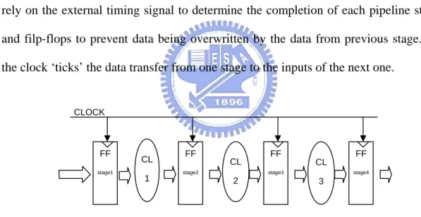
2.1.1 Synchronous Circuit
Figure 2.1 shows a synchronous circuit. For simplicity the figure shows a pipeline, but it is intended to represent any synchronous circuit. Synchronous circuits rely on the external timing signal to determine the completion of each pipeline stage and filp-flops to prevent data being overwritten by the data from previous stage. As the clock ‘ticks’ the data transfer from one stage to the inputs of the next one.
FF stage1 FF stage2 CL 1 FF stage3 FF stage4 CL 3 CL 2 CLOCK
Figure 2.1 Synchronous circuit
Pipeline
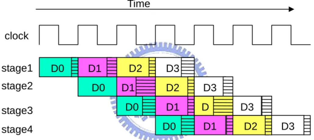
Figure 2.2 shows the synchronous pipeline execution diagram. The shaded areas
2.1.2 Synchronous
of each stage represent the stage having completed its computation and the result being valid but waiting for the clock before moving to the next stage. When “D0” passes through stage 1, its results is ready before the next clock edge arrives. During this time period (the shaded area) the data is unable to progress to the next stage.
When “D0” passes through stage 2, it requires entire clock cycle to complete the operation. This operation is known as the worst case pipeline stage. The system clock time is determined by this worst-case-pipeline-stage delay. If the clock frequency is increased, the operation may fail because the result of the logic operation would not be ready in time to be transfered into next stage. This forces the clock to be slower to guarantee the correct operation. Additional to this performance hit the chip will run slower at a higher temperature or a lower voltage so these parameters have to be considered when choosing a clock speed.
clock stage1 stage2 stage3 stage4 D0 D0 D0 D0 D1 D1 D1 D1 D2 D2 D D2 D3 D3 D3 D3 Time
Figure 2.2: Synchronous pipeline occupancy diagram
2.2 Asynchronous Circuits
An asynchronous Circuit is a digital circuit in which the parts are
communicated by a handshake protocol.
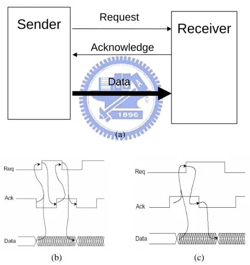
2.2.1 Handshake Protocols
There are several methodologies to realize the asynchronous protocols. These protocols can mainly be divided into two different categories, signaling and data
encoding. From viewing of figure 2.3, we can easily divided encoding schemes into Bundled Data (or Signal Rail) and Dual-Rail (or 1-of-2), each of it can be combined with 2-phase (or NRTZ) or 4-phase (or RTZ) signaling protocols. Therefore, we have two-phase signal-rail, four-phase signal-rail, two-phase dual-rail, four-phase dual-rail asynchronous handshaking protocols.
Figure 2.3: Asynchronous handshake protocols
The Bundled Data (BD) or called Single Rail (SR) refers to separate request and acknowledge wires that bundles the data signals with them (figure 2.24(a)). The data wires carry conventional data signals. Figure 2.4(b) shows the 4-phase bundled data protocol. The sender places a data value on the data wires and produces an event on its one of the control wire called “request” to indicate that the data are available. After the receiver receiving the request event, the receiver sends an event called “acknowledge” to the sender to indicate the data have been accepted. After the sender receives the acknowledge signal, it falls the request signal to indicate for preparing next transfer. Finally, when the receiver gets the request low signal, it will send the acknowledge signal low to tell sender that it can transfer next data.
Another solution is the 2-phase bundled data methodology [7] shown in figure 2.4(c). The “2-phase” indicates that only two phases of the operation: the sender’s active phase and receiver’s active phase. First, the sender places a data on the data
wires and then indicates an event on request wire to tell the receiver that the data is ready. After the receiver has received the data completely, it produces an acknowledge event to the sender. When the sender receives the acknowledge signal, it is able to prepare the data for next transferring.
All the bundled-data protocols rely on the delay matching. That is, the sender must make sure that the data signals are ready for the receiver before it can send the request event.
) to
Sender
Request
Receiver
Acknowledge
Data
(a)
(b) (c)
Figure 2.4: Bundled Data channel (a); 4-phase bundled-data protocol (b); 2-phase bundled-data protocol (c).
Except bundled data method, another choice is to use a more sophisticated protocol that is robust to wire delay. The most important of all is the dual-rail encoding method. The idea of dual-rail encoding method will be introduced in the
following section.
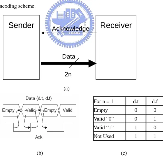
Dual-Rail Encoding Method
To represent 1-bit data in dual-rail encoding method, two physical wires are used. For example, a valid data, D is represented by two physical data wires, d.t and d.f. The following equation shows this encoding scheme.
D = 0 ; (d.t,d.f) = (0,1) D = 1 ; (d.t,d.f) = (1,0).
In particular, (t,f) represents a space which allows us to identify consecutive 0's or 1's. (1,1) state is not used. Data transferring starts from the (0,0) state (called “null” or “empty” data). If a state is changed from (d.t,d.f) = (0,0) to (0,l)/(1,0), which notices the arrival of valid data '0/l'. Figure 2.5 (c) shows how a valid bit is represented in dual-rail encoding scheme.
Sender
Acknowledge
Receiver
Data
2n
(a) For n = 1 d.t d.f Empty 0 0 Valid “0” 0 1 Valid “1” 1 0 Not Used 1 1 (b) (c)Figure 2.5: 4-phase dual-rail channel (a) ; 4-phase dual-rail protocol (b) ; 1-bit channel encoding chart
The 4-phase dual-rail channel encodes the request signal into the data signals using two wires per bit as shown in figure 2.5 (a). The sender does not need to send request signal any more, and the receiver has to detect when the data is valid.
The abstract view of 4-phase handshake as shown in figure 2.5 (b): (1) the sender sends valid data to the receiver, (2) the receiver absorbs the valid data and sets the acknowledge signal high, (3) after the sender announced by acknowledge, it sets the data out to be empty value, (4) the receiver responses this by setting acknowledge signal low and at this time the sender may initiate next communication cycle.
2.2.2 Classification of Asynchronous Circuits
Asynchronous circuits can be classified into delay-insensitive, quasi-delay-insensitive, speed-independent and self-timed depending on the delay assumptions that are used [2].
(1) Delay-Insensitive (DI): A circuit that operates “correctly” with positive, bounded but unknown delay in wires as well as in gates. Such circuits are obviously extremely robust. However, the class of DI circuits is rather small. Only circuits composed of C-elements and inverters can be delay-insensitive.
(2) Quasi-Delay-Insensitive (QDI): Circuits that are delay-insensitive with the exception of identified wire forks. An output of the gate forks some wires, then these wires have the same delay time at all end-points. Such wire fork is called isochronic
fork.
(3) Speed-Independent (SI): A circuit that operates “correctly” with positive, bounded but unknown delay in gates and ideal zero-delay in wires.
(4) Self-Timed: circuits whose correct operation relies on more elaborate and/or engineering timing assumptions.
2.2.3 The Advantages of Asynchronous Circuits
The major difference between asynchronous circuits and synchronous circuits is on the use of the global clock. Asynchronous circuits run without a global clock and each block is communicated via a protocol. This makes the asynchronous circuits have some advantages in comparison with the synchronous circuits [2].
(1) High Performance:
The performance of the synchronous circuit is determined by the slowest block. This makes the synchronous circuits run at worst-case performance. However, in an asynchronous circuit, the next computation step can be started immediately after the previous step has been completed. There is no need to wait for a transition of the clock signal. This leads, potentially, to a fundamental performance advantage for asynchronous circuits, an advantage that increases with the variability in delays associated with these computation steps.
(2) Low Power Dissipation:
In asynchronous systems each block or gate only consumes energy when and where active. After completion of its tasks, it returns to a non-active state and almost no power is consumed.
(3) Low Noise and Low EMI:
Due to the absence of a clock, asynchronous circuits may have better noise and EMC properties than synchronous circuits.
(4) Better modularity:
In an asynchronous circuit, the different modules can be integrated easily by the handshake protocol without concerning of the clock timing.
(5) Robustness towards variations in environment:
environment and supply voltage. Because of the clock, synchronous designs have to attend the environment variation to allow correct operation. Asynchronous circuits can operate correctly under higher range for environment variations.
2.3 Asynchronous Pipeline
There are several asynchronous pipeline implementation styles have been purposed. One of the important circuits is the Muller pipeline. It is built from C-elements and inverters. Another well known circuit is called Micropipelines, which is 2-phase bundled data protocol, introduced by Ivan Sutherland in his Turing Award Lecture [7]. Other asynchronous pipeline implementations use different circuit design methods to replace the C-element and latch, such as “Fine-Grain Dynamic Datapaths” at Columbia University [9], “GASP” at Sun Microsystems Lab [8]. Because of our design, we will introduce the C-element and 4-phase dual-rail pipeline.
2.3.1 C-element
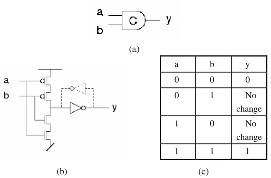
The Muller C-element is a very commonly used component in designing asynchronous circuits [10]. Figure 2.6 shows the symbol, construction and truth-table of a two input C-element. When all of the inputs of a C-element are low, the output will be low; when two inputs of a C-element are high, the output will be high; otherwise the output will remain unchanged. With this property, the C-element sometimes can be used as a storage element.
(a) a b y 0 0 0 0 1 No change 1 0 No change 1 1 1 (b) (c)
Figure 2.6: C-element: (a) symbol; (b) possible implementation; (c) truth-table.
2.3.2 4-phase dual-rail Pipeline
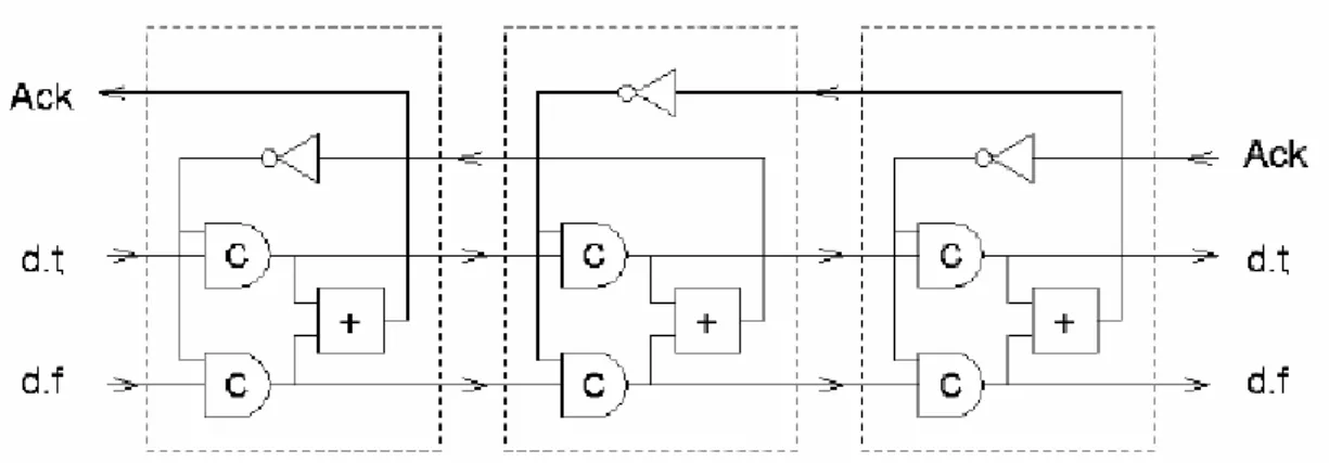
A 4-phase dual-rail pipeline is based on the Muller Pipeline; however the request signal can be eliminated by the dual-rail encoding of data. Figure 2.7 shows the implementation of a 1-bit wide and three stage pipeline without data processing.
To construct circuits with this protocol, gates and data storing elements are required. Each stage can be considered as a dual-rail half latch. This latch is used to store the data similar to a master slave flip-flop in a synchronous circuit. In the initial state, each stage is in null state (null codeword {d.t, d.f} = {0, 0}) which means the output of C-element in each stage is low. The null data causes acknowledge signal low. After the signal pass through an inverter, one of the input of the C-elements in each stage is high. At this moment, the stage is ready to accept the data codeword {0, 1} or {1, 0}. After receiving a valid data codeword, the acknowledge signal turns to high to indicate the previous stage that it has to accept null data. We should notice that because the codeword {1, 1} is illegal and does not occur, the acknowledge signal generated by the OR gate safely indicates the state of the pipeline stage as
being “Data” or “Null”.
Figure 2.7: A 3 stages (1-bit wide) pipeline
An N-bit wide pipeline can be implemented by using a number of 1-bit pipelines in parallel. If bit-parallel synchronization is needed, the individual acknowledge signals can be combined into one global acknowledge with a C-element. Figure 2.8(a) shows a 3-bit wide latch. The OR gates and the C-element in the dashed box form a “completion detector” that indicates whether the 3-bit dual-rail codeword stored in the latch is valid data or null data. Figure 2.8(b) shows an alternative completion detector that uses only a 2-input C-element.
(a) (b)
Figure 2.8: (a) A 3-bit latch with completion detection; (b) Alternative completion detector
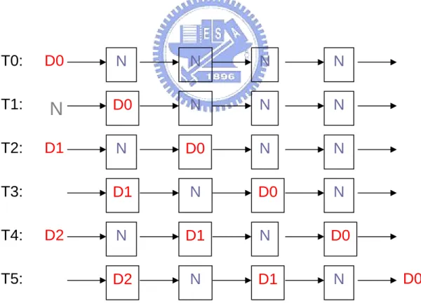
Figure 2.9 explains how data can pass through each pipeline stage and with a 4-pipeline stages implementation. At time T0, it has to initialize the pipeline stages and each stage is in null state. The data codeword “D0” is prepared to send into the first stage. At time T1, the data D0 enters the first stage and it is processed by the combinational logic at stage 1. At time T2, the stage 2 accepts the data codeword and then generates an acknowledge signal to inform stage 1 for accepting the null codeword. This is how the 4-phase dual-rail protocol returns to zero. The RTZ protocol forces data to be followed with a return to zero which can be thought of a null signal. Finally, the data D0 finishes at time T5. From the time period T3 to T5, we can find out that the maximum data occupancy is half of the pipeline stage. In other words, the utilization of the pipeline is 50%.
N
N
N
N
Figure 2.9 Abstract view of data flow
D0
N
N
N
N
D0
N
N
D1
N
D0
N
N
D1
N
D0
D2
N
D1
N
D0
D1
D0
D2
T0:
T1:
T4:
T2:
T3:
T5:
N
Chapter 3: Asynchronous PIC18 Design
3.1 Introduction of Microchip’s PIC18
microcontroller
The PIC18 is a family of high performance, CMOS, fully static, 8-bit MCUs developed by Microchip [16]. All PIC18 MCUs incorporate an advanced RISC architecture. The PIC18 has enhanced core features, 32 level-deep stacks, and multiple internal and external interrupts sources. The separate instruction and data busses of the Harvard architecture allow a 16-bit wide instruction word with the separate 8-bit wide data. The two-stage instruction pipeline allows all instructions to execute in a single cycle, except for program branches, which require two cycles. A total of 77 instructions (reduced instruction set) are available. Additionally, a large register set gives some of the architectural innovations used to achieve a high performance.
3.1.1 System Architecture
Figure 3.1 shows the PIC18 system block diagram. We describe the main parts of PIC18 in the following section.
1. Memory:
PIC18 has a built in program memory (up to 2MB) and a data memory (up to 4KB). The program memory and data memory size are different in each parts.
2. I/O ports and peripherals:
Depending on the device selected and features enabled, there are up to five ports available. Some pins of the I/O ports are multiplexed with an alternate function from
the peripheral features on the device. 3. Multiplier:
By making the multiply a hardware operation, it completes in a single instruction cycle. This is an unsigned multiply that gives a 16-bit result. The result is stored into the 16-bit product register pair.
Figure 3.1: PIC18 microcontroller block diagram
3.1.2 Data Memory Map
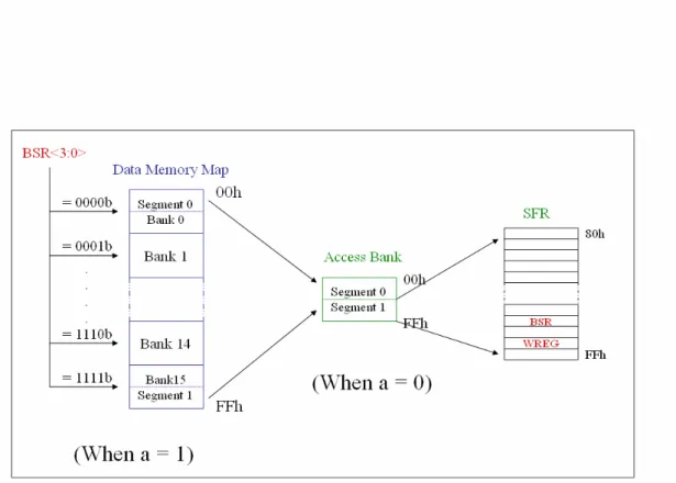
The Data Memory Map has 16 banks of 256 bytes. The Instruction Set and architecture allows operations across all banks (such as MOVFF). A Segment of Bank 0 and a segment of Bank 15 comprise the access bank, as shown in figure 3.2.
<> Access Bank:
compiler code optimization. The access bank is comprised of 2 segments: Segment 0 and Segment 1. Segment 0 is the RAM that is mapped in Bank 0. Segment 1 is the SFRs that are mapped in Bank 15. The sum of RAM mapped by Segment 0 and Segment 1 is 256 bytes. When forced in the access bank (a = ’0’), the last address in Segment 0 is followed by the first address in Segment 1. Segment 1 maps the Special Function Registers so that these registers can be accessed without any software overhead.
Figure 3.2: The Data Memory Map and the Access Bank
3.1.3 Instruction Set
The PIC18 instruction set adds many enhancements to the previous PICmicro (other families, such as PIC13, PIC16 …) instruction sets, while maintaining an easy migration from these PICmicro instruction sets.
instructions that require two program memory locations.
Each single-word instruction is a 16-bit word divided into an opcode, which specifies the instruction type and one or more operands, which further specify the operation of the instruction.
The instruction set is highly orthogonal and is grouped into four basic categories, the detail lists in table 3.1:
• Byte-oriented operations • Bit-oriented operations • Literal operations • Control operations
Most byte-oriented instructions have three operands: 1. The file register (specified by ‘f’)
2. The destination of the result (specified by ‘d’) 3. The accessed memory (specified by ‘a’)
The file register designator ‘f’ specifies which file register is to be used by the instruction. The destination designator ‘d’ specifies where the result of the operation is to be placed. If ‘d’ is zero, the result is placed in the WREG register. If ‘d’ is one, the result is placed in the file register specified in the instruction.
All bit-oriented instructions have three operands: 1. The file register (specified by ‘f’)
2. The bit in the file register (specified by ‘b’) 3. The accessed memory (specified by ‘a’)
The bit field designator ‘b’ selects the number of the bit affected by the operation, while the file register designator ‘f’ represents the number of the file in which the bit is located.
• A literal value to be loaded into a file register (specified by ‘k’)
• The desired FSR register to load the literal value into (specified by ‘f’) The control instructions may use some of the following operands:
• A program memory address (specified by ‘n’)
• The mode of the CALL or RETURN instructions (specified by ‘s’)
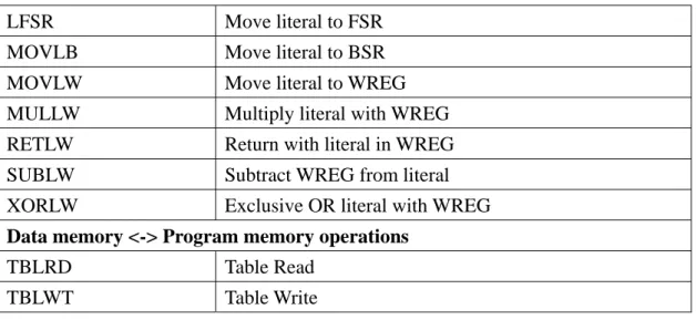
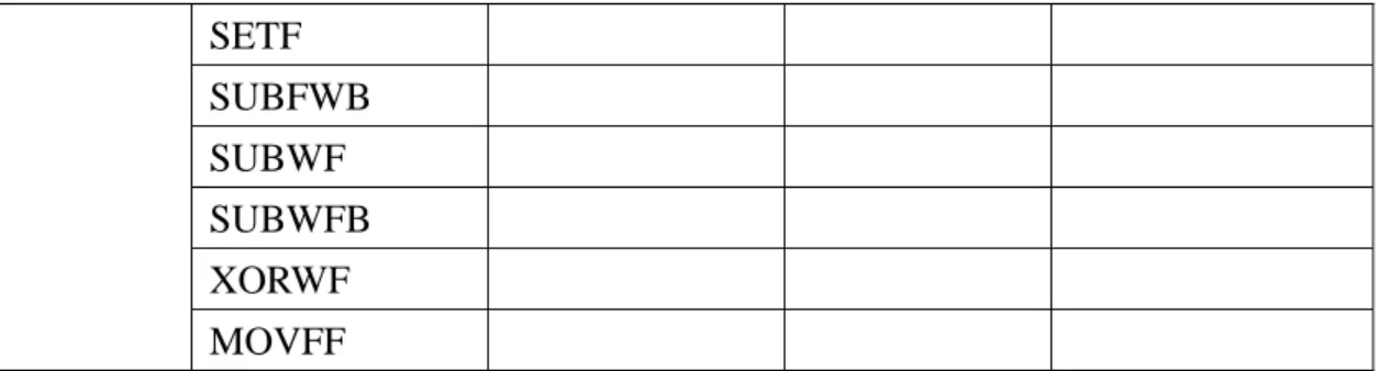
Instruction Description
Byte-Oriented
ADDWF Add WREG and f
ADDWFC Add WREG and Carry bit to f ANDWF AND WREG with f
CLRF Clear f
COMF Complement f
CPFSEQ Compare f with WREG, skip = CPFSTG Compare f with WREG, skip > CPFSLT Compare f with WREG, skip <
DECF Decrement f
DECFSZ Decrement f, skip if 0 DECFSNZ Decrement f, skip if not 0
INCF Increment f
INCFSZ Increment f, skip if 0 INFSNZ Increment f, skip if not 0 IORWF Inclusive OR WREG with f
MOVF Move f
MOVFF Move fs(source) 1st word to fd 2nd word MOVWF Move WREG to f
MULWF Multiply WREG with f
NEGF Negate f
RLCF Rotate Left f through Carry RLNCF Rotate Left f (No Carry) RRCF Rotate Right f through Carry RRNCF Rotate Right f (No Carry)
SETF Set f
SUBFWB Subtract from WREG with borrow SUBWF Subtract WREG from f
SUBWFB Subtract WREG from f with borrow SWAPF Swap nibbles in f
TSTFSZ Test f, skip in f
XORWF Exclusive OR WREG with f
Bit-Oriented
BCF Bit Clear f BSF Bit Set f
BTFSC Bit Test f , skip if Clear BTFSS Bit Test f , skip if Set
BTG Bit Toggle f
Control
BC Branch if Carry BN Branch if Negative BNC Branch if Not Carry BNN Branch if not Negative BNOV Branch if not overflow BNZ Branch if not Zero BOV Branch if Overflow
BRA Branch Unconditionally BZ Branch if Zero
CALL Call Subroutine
CLRWDT Clear Watch Dog Timer
DAW Decimal Adjust WREG
GATO Go To Address
NOP No Operation
POP Pop Top of Return Stack PUSH Push top of return stack
RCALL Relative Call RESET Software device Reset
RETFIE Return from Interrupt enable RETLW Return with literal in WREG RETURN Return from Subroutine SLEEP Go into Standby mode
Literal Operation
ADDLW Add literal and WREG
ANDLW AND literal and WREG IORLW Inclusive OR literal with WREG
LFSR Move literal to FSR MOVLB Move literal to BSR MOVLW Move literal to WREG MULLW Multiply literal with WREG RETLW Return with literal in WREG
SUBLW Subtract WREG from literal XORLW Exclusive OR literal with WREG
Data memory <-> Program memory operations
TBLRD Table Read
TBLWT Table Write
Table 3.1: The PIC18 Instruction Set
3.2 Asynchronous PIC18 microprocessor
architecture
Asynchronous PIC18 is a pipelined 8-bit processor based on 4-pashe dual-rail handshake protocol and QDI delay model. The system block is shown in figure 3.3.
Instructions are executed through 4 stages, namely, IF (Instruction Fetch), ID (Instruction Decode), OF (Operand Fetch) and EX/WB (Execution and Write Back). The pipeline structure is also shown in system block diagram.
We implemented the register sets only for those which are frequently used, such as PC (Program Counter), BSR (Bank Select Register), WREG (Working Register), STATUS (for flags), STKPTR (Stack Pointer) and Stall (for instruction stall). Some PIC18 registers were not implemented, because those registers are not used frequently or related to peripherals.
3.2.1 Instruction Set
The instruction set of asynchronous PIC18 is compatible with Microchip’s PIC18 family. However, some instructions were not implemented due to not implemented peripherals. The instructions we have implemented is shown in table 3.2.
Operation Byte-Oriented Bit-Oriented Literal Control
ADDWF BCF ADDLW BC
ADDWFC BSF SUBLW BNC ANDWF BTG MULLW BN
ANDWF MOVLB BNN
COMF MOVLW BOV
DECF IORLW BNOV
INCF ANDLW BZ IORWF XORLW BNZ MOVF BRA MOVWF GOTO MULWF CALL NEGF RETURN RLCF PUSH RLNCF POP RRCF RCALL instruction RRNCF NOP
SETF SUBFWB SUBWF SUBWFB XORWF MOVFF
Table 3.2: Asynchronous PIC18 instruction sets
3.2.2 Construction of the Basic Elements
The first element we built is a C-element; figure 3.4 shows the CMOS
transistor-level design. Base on the C-element, we can construct the dual-rail OR gate and dual-rail AND gate.
Figure 3.4: COMS transistor implementation for a generalized C-element
The RTZ protocol needs to separate its valid data signals between null signals. Creating logic using this protocol, the output should become valid data codeword only when all the inputs are valid data. Also the output should remain as valid data until all the inputs have returned to zero. Figure 3.5 shows the construction of a dual-rail OR gate with this needs. The row of C-elements forces both of the inputs to switch before the output switches. The return to zero protocol assumes that once a gate outputs a
valid signal then all its inputs are valid. Also the data will not return to zero until all inputs have returned to zero.
Figure3.5: Dual-rail OR gate symbol and schematic
3.2.3 Pipeline latch
Our pipeline latches use the same as the Muller Pipeline design shown in Figure 3.6. If there is no acknowledgement on the input from next stage (Ack_in is low) any valid data on the input will progress through the C-elements to the output. Once one of the data outputs is active the latch will acknowledge its input (Ack_out is high). The data output line will stay valid until the target acknowledges and the source has returned to zero. Once the outputs have finished the process the then Ack_in turns to high. The next stage is ready to accept null data. At this time, the inputs have to send the null data. If these latches are placed in a pipeline then the maximum occupancy would be 50% as for each latch that holds data, another separates the data with a null from other data in the pipeline.
Din.t
Din.f
Dout.t
Dout.f
Ack_out
Ack_in
Figure 3.6: Pipeline latch (1-bit)
3.2.4 Design for each Stage
After constructing several basic dual-rail gates, such as C-element, AND and OR, we continued to build some other needed components, such as multiplexer, demultiplexer, encoder etc. based on those basic dual-rail gates. Then, we used these gates and modules to construct the whole processor.
IF stage:
In the IF stage, the “Read” signal controls the output for valid data or null data. When the Read signal is high, it reads PC value from the PC register and then retrieves the instructions from the program ROM. In addition, the current PC value is sent to ID stage for calculating the next PC value. After the output data has completely sent to pipeline latch, the pipeline latch returns a acknowledge signal. We use this signal to indicate that the Read signal changes to low, and then the IF stage becomes null state.
Figure 3.7: Block diagram of the IF stage
ID stage:
Figure 3.8 shows the block diagram of the ID stage. The purposes of each inner block describe as following:
Instruction Decode: Decoding input of instruction and generating control signals for inner block, OF or EXE/WB stage control.
Branch Control: If the current instruction is the branch relative instruction, the Instruction Decode will generate a control signal to the Branch Control. The Branch Control reads STATUS register value to decide this branch is taken or non-taken and then send control signal to NPC Control.
Stall Control: If the instruction is what we called two cycle instruction such as branch
which needs STATUS register value at ID stage, we will control NPC value to read this instruction again. We use this stall mechanism to make
stage and STATUS register value read in ID stage is correct.
MPC Control: This block receive information and generate next PC value to the PC register.
Figure 3.8: Block diagram of the ID stage
OF stage:
The main purpose of the OF stage is to prepare source and destination information for EXE/WB stage. Figure 3.9 shows the block diagram of the OF stage. The left of the stage are input signals from ID stage. The top of the stage are input/output signals from/to registers. The bottom of the stage is the data memory interface. The right of the stage is output signals to EXE/WB stage.
Source1 contains data in data memory. Some special function registers in the data memory have been mapped into real registers. That means if the accessed
memory address is access for special registers, the data is directly retrieved from these registers without any data memory accesses. Therefore, S1 selects data from register or data memory.
Source2 contains the WREG value or the Bit-Op information.
Carry signal is used for some instructions that need the carry bit, such as “rotate left with carry”.
Destination signal gives EXE/WB stage information about where the calculate result should be written.
Figure 3.9: Block diagram of the OF stage
The inner blocks of the OF stage are described as following:
Bank Select Control: If access bank is enabled, it reads the 4-bit BSR value and concatenates with 8-bit address in instruction. The final 12-bit
is disabled, the data memory can be read only in segment-0 of bank-0 or segment-1 of bank-15.
Register Address Mapping: In synchronous PIC microcontroller registers are located in data memory. In our asynchronous PIC design, we implemented real registers instead of the registers in data memory due to reducing the memory accesses. The Register Address Mapping unit is used to detect if the memory access fetches the register, it changes the access to our duplicated registers. Bit-Op Control: To indicate which bit to be modified, only used in bit operation
instructions.
3.2.5 Memory
Although our asynchronous PIC18 is based on QDI delay model, the main storage does not follow this model. In order to access the conventional memory, we added a dual-rail to single-rail converter, a single-rail to dual-rail converter and matching delay as the interface to memory.
The system block is shown in figure 3.10 (a). Figure 3.10 (b) is a dual-rail to single-rail converter and figure (c) is a single-rail to dual-rail converter. After the address sends to 2-1 converter, the completion detector will generate a “strobe” signal. The “strobe” through a delay and then control the output of the 1-2 converter. The delay time has to be longer than the memory data read out time to make sure the output data is correct.
Figure 3.10: Program ROM interface: block diagram (a); dual-rail to single-rail converter (b); single-rail to dual-rail converter.
3.2.6 Register
To accommodate QDI requirement our asynchronous PIC18 was implemented without common bus. Data transfers from one block to the register use a direct data path. Thus, one important thing is to design a dual-rail asynchronous register that match the property of our design. Figure 3.11 illustrates a 1-bit dual-rail register which is modified from the design of the TITAC [12].
When data codeword ({0, 1} or {1, 0}) is sent to din.t and din.f, the two NOR gates can hold the data on their output. When the data is written into this register, it issues an ACK signal as completion signal to inform the previous stage that the writing action is done.
For a read operation, just send a “read” signal and the dual-rail data can be read out correctly.
Ack
read
dout.f
/read
dout.t
din.t
din.f
3.2.7 Reset circuit
Before the reset signal is applied, the latches can hold random data and gates may have some unknown values. In order to eliminate these random data in the beginning of the circuit operation, constructing the resetting circuit with minimum hardware cost is important. Our approach is to attach a reset line to all C-elements and thus forcing all nets in the circuit to reset. If all inputs to a dual-rail gate are low then the output will switch to low. Using this assumption, it is possible to reset the whole circuit to nulls state by just resetting all latches.
Figure 3.1 shows the CMOS transistor-level of resetable C-element design. The resetable C-element is only used for designing the pipeline latches.
3.3 Design Flow
Figure 3.13 shows our design flow of the asynchronous PIC. First of all, the asynchronous PIC specifications have to be defined. The specifications of the instructions refer to the synchronous PIC18 and the handshake protocol is 4-phase dual-rail with QDI timing assumption.
Secondly, Verilog HDL is used to build the dual-rail logic gates. Based on these dual-rail logic gates, we can construct the frequently used modules such as MUX, DEMUX and decoder etc. Then, the functional blocks needed of our asynchronous PIC18 were constructed with them.
Finally we construct the whole system with these functional blocks.
Chapter 4: Simulation Result
In order to verify the correctness of out asynchronous PIC design, we wrote some simple programs. Table 4.1 shows one of the examples. This program runs a loop and each time the WREG register is added by 1.
Memory address Assembly code Description 00000000 MOVLW 1 WREG <= 1 00000010 MOVWF f(0),0 f(0) <= WREG
00000100 ADDWF f(0),1,0 WREG <= WREG + f(0) 00000110 GOTO 00000100 PC <= 00000100
Table4.1: A simple test program.
The Modelsim software is used to simulate the function of our system and verify the correctness of the instruction execution. Figure 4.1 shows the wave form of the simulation. In the example we verified the results by reading signals of the WREG register.
4.1 Performance
In order to synthesis our asynchronous PIC design, we have to modify our MOS level C-element to an AND-OR gate level code. Figure 4.2 shows the maximum path delay in each stage or block. The simulation result is based on Altera Cyclone EP1C20F300C8 FPGA.
Module Maximum Path Delay ( ns ) Latch ~ 34 IF stage ~ 27 ID stage ~ 455 OF stage ~ 157 EX/WB stage ~ 216 Register ~ 19 Figure 4.2: Maximum path delay for each stage.
From this result, our critical path of asynchronous PIC design is in ID stage. In ID stage, not only has to decode the instructions but also need to handle the branch instructions. Obviously, if we want to improve our performance, the branch handling mechanism has to be carefully implemented.
4.2 Area
In order to compare with our design, we choose an open source implementation which is a synchronous version of the PIC processor written by the Verilog and can be downloaded into FPGA [11]. The Altera Quartus II software is used to synthesis async. and sync. circuits, and the target device is based on Cyclone EP1C20F400C8 which is a 1 million gate counts ( or 20,000 logic elements) FPGA. The comparison result is shown in Table4.2.
Asynchronous PIC Synchronous PIC Logic Elements ~ 13,800 ~ 3,900
Table4.2: The gate count comparison
The result shows that our asynchronous PIC uses about 3.5 times logic element than the synchronous version. It is caused by two reasons. One is our design style which is dual rail data encoding method. The other is branch handling. In our asynchronous PIC, the branch instructions are determined in ID stage. This makes the ID stage to use more logic circuits to handle it.
Chapter 5: Conclusions
In this thesis, we have presented a traditional synchronous design tool “Verilog” for implementing the asynchronous PIC microprocessor. Our asynchronous PIC can run most of the instructions of PIC18 ISA.
The PIC18 is widely used in embedded system design. However, there are not many resources we can obtain for comparing with our asynchronous design. Thus, we just verified the correctness of the function and compared the cost with a synchronous implementation so far.
Our design is based on QDI delay model. However, it is still great benefit needed if we wish to realize it with a real chip.
We will implement the full function of the interrupt mechanism, optimize the system blocks, and finally realize the design with real chip in the future.
References
[1] Alain J. Martin. "Synthesis of Asynchronous VLSI Circuits. Formal Methods f o r VLSI Design."J. Staunstrup, North-Holland, 1990.
[2] C.H. van Berekl, M.B. Josephs, and S.M. Nowick. “Scanning the technology: Applications of asynchronous circuits.” Proceedings of the IEEE. 87(2):223-233, February 1999.
[3] Elston, C.J.; Christianson, D.B.; Findlay, P.A.; Steven, G.B. “HADES-an
asynchronous superscalar processor”; Design and Test of Asynchronous Systems,
IEE Colloquium. 28 Feb 1996 Page(s):10/1 - 10/6
[4] H. van Gageldonk, K. van Berkel, A. Peeters, D. Baumann, D. Gloor, and G. Stegmann,” An asynchronous low-power 80C51 microcontroller,” pp. 96, 1998
[5] Hauck S., “Asynchronous Design Methodologies: An Overview “, Proceedings of the IEEE, 83(1):69-93, January 1995.
[6] Spars, J., Furber, S., “Principles of Asynchronous Circuit Design - A Systems Perspective” Kluwer Academic Publishers, Hardcover ISBN 0-7923-7613-7, 2001 [7] I. Sutherland, “Micropipelines,” Communications of the ACM, Volume 32, No. 6,
pp. 720-38, June 1989.
[8] I. Sutherland and S. Fairbanks, "GasP: a minimal FIFO control," Asynchronous Circuits and Systems, 2001. ASYNC 2001. Seventh International Symposium on, 2001.
[9] Montek Singh, Steven M. Nowick, “High-Throughput Asynchronous Pipelines for Fine-Grain Dynamic Datapaths”, ASYNC 2000, p198,
[10] D. E. Muller and W. S. Bartky. “A theory of asynchronous circuits.” In
Proceedings of an International Symposium on the Theory of Switching, pages
[11] Shawn Tan, “AE18 CPU CORE”, www.opencores.org/projects/ae18, 2003
[12] Takashi Nanya, Yoichiro Ueno, Hiroto Kagotani, Masashi Kuwako, and Akihiro Takamura. “TITAC: Design of a quasi-delay-insensitive microprocessor”. IEEE Design & Test of Computers, 11(2):50--63, Summer 1994.
[13] A. Takamura, M. Kuwako, et al. “TITAC-2: An Asynchronous 32-bit Microprocessor based on Scalable-Delay-Insensitive Model”. ICCD 1997, 288-294.
[14] J.V. Woods, P. Day, S.B. Furber, J.D Garside, N.C. Paver, S. Temple,
“AMULET1: an asynchronous ARM microprocessor", IEEE Transactions on Computers, Volume: 46 Issue: 4, pp. 385 – 398, April 1997.
[15] Yuan-Teng Chang, Master’s Thesis, “SA8051: An Asynchronous Soft-core Processor for Low-Power System-On-Chip Application.” National Chiao Tung University, 2005.