Low-etch-pit-density GaN substrates by regrowth on free-standing GaN films
Chiung-Chi Tsai, Chen-Shiung Chang, and Tsung-Yu Chen
Citation: Applied Physics Letters 80, 3718 (2002); doi: 10.1063/1.1480108 View online: http://dx.doi.org/10.1063/1.1480108
View Table of Contents: http://scitation.aip.org/content/aip/journal/apl/80/20?ver=pdfcov
Published by the AIP Publishing
Articles you may be interested in
Reduction of dislocation density in epitaxial GaN layers by overgrowth of defect-related etch pits
Appl. Phys. Lett. 95, 031913 (2009); 10.1063/1.3171928
Characterization of free-standing hydride vapor phase epitaxy GaN
Appl. Phys. Lett. 78, 2297 (2001); 10.1063/1.1359779
Characteristics of free-standing hydride-vapor-phase-epitaxy-grown GaN with very low defect concentration
Appl. Phys. Lett. 77, 3743 (2000); 10.1063/1.1330563
Low-dislocation-density GaN from a single growth on a textured substrate
Appl. Phys. Lett. 77, 3233 (2000); 10.1063/1.1325394
GaN homoepitaxy by metalorganic chemical-vapor deposition on free-standing GaN substrates
Appl. Phys. Lett. 77, 1858 (2000); 10.1063/1.1311596
This article is copyrighted as indicated in the article. Reuse of AIP content is subject to the terms at: http://scitation.aip.org/termsconditions. Downloaded to IP: 140.113.38.11 On: Thu, 01 May 2014 06:19:18
Low-etch-pit-density GaN substrates by regrowth on free-standing
GaN films
Chiung-Chi Tsai and Chen-Shiung Changa)
Institute of Electro-Optical Engineering, National Chiao-Tung University, Hsinchu, Taiwan, Republic of China
Tsung-Yu Chen
Advance Eepitaxy Technology, Hsinchu, Taiwan, Republic of China
共Received 19 November 2001; accepted for publication 18 March 2002兲
In this study, GaN substrates with low-density etch pits were obtained by regrowth on free-standing GaN films共two steps兲 by hydride vapor-phase epitaxy 共HVPE兲. The etch-pit density was lower than 4⫻104 cm⫺2 by atomic-force microscopy. The density is significantly lower than that of the HVPE-grown 共one-step兲 GaN films 共HVPE GaN兲, using sapphire as a substrate. The optical and electrical properties of the two-step HVPE-grown GaN substrates are superior to those of HVPE GaN. Temperature-dependent photoluminescence measurements reveal that thermal quenching behavior of the 2.9 eV band is possibly attributed to a shallow acceptor level at about 118
⫾5 meV above the valence band. © 2002 American Institute of Physics. 关DOI: 10.1063/1.1480108兴
GaN is a promising material for optoelectronic device applications such as laser diodes and light-emitting diodes in the visible and ultraviolet spectrum as well as for electronic devices, due to its wide band gap and good thermal stability.1 Because of lack of native substrates, these semiconductor devices have been grown on many alternative substrates such as sapphire and SiC. However, a large lattice mismatch is present between the GaN epitaxial layer and the foreign sub-strate, resulting in a large number of dislocations. Accord-ingly, sapphire and SiC give rise to a very large dislocation density, in the range of 108– 1010 cm⫺2.2 In addition, the thermal expansion coefficient of the GaN film differs from that of the foreign substrate, giving rise to stress and bowing during heteroepitaxial growth. Using a GaN substrate would be a total solution to the problems mentioned above. Hydride vapor-phase epitaxy 共HVPE兲, sublimation, and a high-pressure method have been applied to obtain GaN bulk crystal.3–5 HVPE is so far the best of all these methods by which to grow thick GaN films because of its high growth rate. The extended defect density 共etch pits兲 of a 300 m GaN film grown by HVPE was recently reported to be 5
⫻105 cm⫺2.6Using GaN as a substrate yields a low thread-ing dislocation density, and hence, improves the performance of the device.7 In this work, we report on the properties of thick GaN substrates, obtained by regrowth on free-standing HVPE GaN.
Free-standing HVPE GaN films were obtained by HVPE growth and laser-induced lift-off. First, 2m templated GaN films共on sapphire兲 grown by metal–organic chemical-vapor deposition共MOCVD兲 were prepared. Next, thick GaN films, referred to as HVPE GaN, with a thickness in the range of 50–200m, were grown on these MOCVD templates using a conventional horizontal-type HVPE system. In this system, HCl reacted with liquid Ga 共850 °C兲 to form GaCl gas and
was then transported into the growth zone area where it di-rectly reacted with NH3 at a temperature of 1050 °C. The growth rate and V/III ratio varied between 50–150m/h and 10–100, respectively. The HVPE-GaN films were then sepa-rated from the sapphire by laser lift-off.8Following chemical cleaning of the surface, the two-step GaN, referred to as the GaN substrate, was obtained by regrowth at a rate of 100
m/h on the free-standing HVPE GaN. GaN substrates have a maximum thickness of 500 m and a typical sample area of 10⫻10 mm2. Schematic diagrams of the MOCVD tem-plate, HVPE GaN, free-standing HVPE GaN, and the GaN substrate are shown in the inset of Fig. 1.
The GaN samples were first examined by double-crystal x-ray diffraction 共DCXRD兲, as shown in Table I. The full
a兲Electronic mail: [email protected] FIG. 1. AFM image ofstanding HVPE GaN, and共a兲 MOCVD template, 共b兲 HVPE GaN, 共c兲 free-共d兲 GaN substrate taken after chemical etching.
APPLIED PHYSICS LETTERS VOLUME 80, NUMBER 20 20 MAY 2002
3718
0003-6951/2002/80(20)/3718/3/$19.00 © 2002 American Institute of Physics
This article is copyrighted as indicated in the article. Reuse of AIP content is subject to the terms at: http://scitation.aip.org/termsconditions. Downloaded to IP: 140.113.38.11 On: Thu, 01 May 2014 06:19:18
width at half maxima共FWHM兲 of the 共0002兲 peak were 250, 160, 220, and 220 arcsec on average for the samples of the MOCVD template, HVPE GaN, free-standing HVPE GaN, and the GaN substrate, respectively. The FWHM of free-standing HVPE GaN is larger than HVPE GaN due to bow-ing of the GaN film after laser lift-off.9Following regrowth, bowing of the GaN film still exists, which makes the FWHM of the GaN substrate more than 200 arcsec.
Room-temperature Hall measurement was also per-formed to study the electrical properties of the GaN samples. Table I also shows the carrier concentration and carrier mo-bility of the GaN samples. Higher momo-bility can be achieved using the regrowth process on free-standing HVPE GaN. The mobility and the electron concentration are around 700–1050 cm2/V s and 1016– 1017cm⫺3, respectively, due probably to the reduction of dislocation density and ionized impurity concentration.10
Prior to atomic-force microscopy 共AFM兲 measurement, chemical etching11 (H3PO4/H2SO4) was undertaken at 250 °C to reveal etch pits in these GaN samples. Figures 1共a兲–1共d兲 show the AFM images obtained from the MOCVD template, HVPE GaN, free-standing HVPE GaN, and the GaN substrate, respectively. Figure 1共a兲 is a typical AFM image of an unintentionally doped MOCVD template. The density of the indicated etch pits is as much as 6
⫻108 cm⫺2. In our HVPE GaN samples, the etch-pit density
共EPD兲 values were between 107and 3⫻108 cm⫺2, as shown in Fig. 1共b兲. Reynolds et al. stated that the defect density as a function of HVPE GaN thickness, declines significantly beyond a thickness of 75m.12For the 500-m-thick GaN substrate, as shown in Fig. 1共d兲, no etch pits can be detected in the AFM image, even in the area of 50m⫻50m. The EPD was estimated to be lower than 4⫻104 cm⫺2which is a low reported density. The density could be tentatively ex-plained as follows. First, the regrowth of GaN on free-standing HVPE GaN leads to a nearly stress-free homoepit-axy, and thus significantly reduces defect density. Second, the thickness of both HVPE GaN and the regrowth GaN films are strongly related to the defect density and the crystal quality.12For example, in order to obtain a high-quality GaN substrate, the defect density of HVPE GaN should be lower than 108 cm⫺2, which corresponds to a thickness above 120
m. Finally, the defect density also depends on the HVPE system used and the growth condition. The corresponding results will be published elsewhere.
Even though the GaN substrate sample shows an EPD lower than 4⫻104 cm⫺2, an earlier report proved that no etch pits formed at the edge or at full core screw dislocations but could form at nanopipes 共open-core screw dislocations兲.13 In order to reconfirm the threading
disloca-tion density of the GaN substrate, 60 and 150 K times plan-view transmission electron microscopy 共TEM兲 was also ob-served by JEOL2000FSII. None of the detectable dislocations could be found from TEM, which are consistent with our AFM data.
The surface roughness 共after etching兲 was also deter-mined from AFM data to be 12.034, 6.482, and 1.186 nm with respect to the samples of the MOCVD template, HVPE GaN, and the GaN substrate, as shown in Fig. 1. Among the three samples, the thick GaN substrate exhibits the smallest surface roughness, probably related to the presence of fewer EPDs and the good quality of the thick GaN film.
Photoluminescence 共PL兲 measurements were obtained by exciting a 325 nm He–Cd laser on the GaN samples. Figure 2 displays low-temperature 共20 K兲 PL spectra of HVPE GaN and the thick GaN substrate. The spectra of the samples demonstrate three peaks located at 3.44, 3.36, and 3.27 eV, which are related to the emission lines from natural donor-bound recombination 共I2 line兲, phonon replica of donor-bound exciton (I2-LO), and natural donor–acceptor-pair recombination (D0A0), respectively.14 The FWHM of the I2line at 3.44 eV, attributable to a transition of an exciton bound to a neutral shallow donor, are 13 and 7.2 meV for HVPE GaN and the thick GaN substrate, respectively. The spectrum also included a broadband with a peak at 2.9 eV, known as the 2.9 eV band, which is related to the defect level.15Following regrowth, the intensity of the 2.9 eV band decreases, implying that the regrowth of GaN on free-standing HVPE GaN can lower the defect density and result in enhancement of the emission line at 3.44 eV.
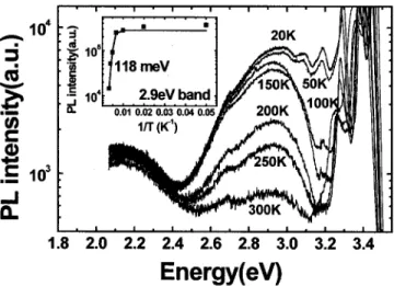
Temperature-dependent PL was also performed for the thick GaN substrate to examine the nature of the weak 2.9 eV band. As shown in Fig. 3, the PL intensity of the 2.9 eV band decreases gradually with increasing temperature from 20 to 150 K. However, the thermal quenching behavior of the 2.9 eV band is observed above 150 K. The activation energy was obtained from the best fit to the experiment data with an Arrhenius plot共inset in Fig. 3兲. The activation energy was then determined to be about 118⫾5 meV above the va-lence band. This is the thermal ionization energy of the shal-low acceptor involved in the 2.9 eV band.15The PL quench-ing above 150 K is attributable to the thermal release of
TABLE I. Listed data of DCXRD and Hall measurements of the MOCVD template, HVPE GaN, free-standing HVPE GaN, and the GaN substrate.
GaN samples FWHM of共0002兲 peak共arsec兲 concentration (1016cm⫺3) 共cmmobility2/V s兲 MOCVD template 200–300 5–15 150–250 HVPE GaN 120–200 1–12 200– 800 Free-standing HVPE GaN 180–250 1–12 200– 800 GaN substrate 180–250 0.8 –10 700–1050
FIG. 2. Low-temperature共20 K兲 PL spectrum of HVPE GaN and the GaN substrate.
3719
Appl. Phys. Lett., Vol. 80, No. 20, 20 May 2002 Tsai, Chang, and Chen
This article is copyrighted as indicated in the article. Reuse of AIP content is subject to the terms at: http://scitation.aip.org/termsconditions. Downloaded to IP: 140.113.38.11 On: Thu, 01 May 2014 06:19:18
holes trapped by the shallow acceptor. The result is different from that of earlier work,15and suggest that the 2.9 eV band involved a transition from a shallow donor level to a deep acceptor level located at 380 meV above the valence band. However, our fitting data suggest that the 2.9 eV band could possibly result from the transition between a deep donor level and a shallow acceptor level located at 118 meV above the valence band. A similar interpretation has also been sug-gested by Kaufmann et al.16The location of the shallow ac-ceptor level is similar to that described in Ref. 17, wherein the two-hole共excited-state兲 transition of acceptor–bound ex-citons led to ground-state energies of 85⫾1 and 115
⫾1 meV. Another group from the calculation of hole’s
ef-fective mass indicated a level of EA⫽120 meV.18 Some
more-detailed calculations further support the inference of the presence of a shallow acceptor level 共100–130 meV兲.19 However, the gallium vacancy VGa or any of its complexes with Si, O, and H could be another possible origin of the 2.9 eV band.20
In conclusion, GaN substrates were obtained by the re-growth process on free-standing HVPE-GaN films. The EPD was determined by AFM to be lower than 4⫻104 cm⫺2. The electrical and optical properties of the GaN substrates are superior to those of HVPE GaN. The PL spectrum reveals
the thermal quenching behavior of the 2.9 eV band. The behavior could be possibly related to the donor-to-acceptor transition involving a shallow acceptor level at 118
⫾5 meV above the valence band.
The authors would like to thank Advance Epitaxy Tech-nology for the material growth and the National Science Council of the Republic of China for financially and experi-mentally supporting this research under Contract No. NSC90-2212-M009-049.
1
S. Nakamura, M. Senoh, N. Iwasa, and S. Nagahama, Jpn. J. Appl. Phys., Part 2 34, L797共1995兲.
2S. D. Lester, F. A. Ponce, M. G. Crawford, and D. A. Steigerwald, Appl. Phys. Lett. 66, 1249共1995兲.
3T. Detchprohm, K. Hiramatsu, H. Amano, and I. Akasaki, Appl. Phys. Lett. 61, 2688共1992兲.
4S. Kurai, Y. Naoi, T. Abe, S. Ohmi, and S. Sakai, Jpn. J. Appl. Phys., Part 1 35, 1637共1996兲.
5I. Grzegory, J. Jum, M. Bockowski, S. Krukowski, M. Wroblewski, B. Lucznic, and S. Porowski, J. Phys. Chem. Solids 56, 639共1995兲. 6
F. Yun, M. A. Reshchikov, K. Jones, P. Visconti, H. Morkoc, and S. S. Park, Solid-State Electron. 44, 2225共2000兲.
7S. Nakamura, M. Senoh, N. Iwasa, T. Yamada, and T. Matsushita, Appl. Phys. Lett. 73, 832共1998兲.
8
M. K. Kelly, R. P. Vaudo, V. M. Phanse, L. Gorgens, O. Ambacher, and M. Stutmann, Jpn. J. Appl. Phys., Part 2 38, L217共1999兲.
9L. Leszczynski, T. Suski, H. Teissryre, P. Perlin, I. Grzegory, J. Jun, S. Porowski, and T. D. Moustakas, J. Appl. Phys. 76, 4909共1994兲. 10D. Hung, F. Yun, M. A. Reshchikov, and D. Wang, Solid-State Electron.
45, 711共2001兲.
11Y. Ono, Y. Iyechika, T. Takada, K. Inui, and T. Matsye, J. Cryst. Growth
189, 133共1998兲.
12D. C. Reynolds, D. C. Look, B. Jogai, J. E. Hoelscher, R. E. Sherriff, and R. J. Molnar, Appl. Phys. Lett. 88, 1460共2000兲.
13
S. K. Hong, T. Yao, B. J. Kim, S. Y. Yoon, and T. I. Kim, Appl. Phys. Lett.
77, 82共2000兲.
14M. Leroux, N. Grandjean, B. Beaumont, G. Nataf, F. Semond, J. Massies, and P. Gibart, J. Appl. Phys. 86, 3721共1999兲.
15
M. A. Reshchikov, F. Shahedipour, R. Y. Korotkov, and B. W. Wessels, J. Appl. Phys. 87, 3351共2000兲.
16U. Kaufmann, M. Kunzer, H. Obloh, M. Maier, Ch. Manz, and B. Santic, Phys. Rev. B 59, 5561共1999兲.
17
D. C. Reynold, D. C. Look, B. Jogai, and R. J. Molnar, J. Appl. Phys. 89, 6272共2001兲.
18J. W. Orton and C. T. Foxon, Rep. Prog. Phys. 61, 1共1998兲.
19J. B. Xia, K. W. Cheah, X. L. Wang, D. Z. Sun, and M. Y. Kong, Phys. Rev. B 59, 10119共1999兲.
20
J. Neugebauer and C. G. Van de Walle, Appl. Phys. Lett. 69, 503共1996兲.
FIG. 3. Temperature-dependent PL spectrum of the GaN substrate.
3720 Appl. Phys. Lett., Vol. 80, No. 20, 20 May 2002 Tsai, Chang, and Chen
This article is copyrighted as indicated in the article. Reuse of AIP content is subject to the terms at: http://scitation.aip.org/termsconditions. Downloaded to IP: 140.113.38.11 On: Thu, 01 May 2014 06:19:18