Cross-sectional transmission electron microscopy observations of structural damage
in Al 0.16 Ga 0.84 N thin film under contact loading
Sheng-Rui Jian, Jenh-Yih Juang, and Yi-Shao Lai
Citation: Journal of Applied Physics 103, 033503 (2008); doi: 10.1063/1.2836939
View online: http://dx.doi.org/10.1063/1.2836939
View Table of Contents: http://scitation.aip.org/content/aip/journal/jap/103/3?ver=pdfcov Published by the AIP Publishing
Articles you may be interested in
Intrusion-type deformation in epitaxial Ti 3 Si C 2 Ti C 0.67 nanolaminates Appl. Phys. Lett. 91, 123124 (2007); 10.1063/1.2789710
Mechanical properties of Al x Ga 1 x N films with high Al composition grown on AlN/sapphire templates Appl. Phys. Lett. 91, 091905 (2007); 10.1063/1.2735551
Mechanical properties of sol-gel derived Bi Sc O 3 – Pb Ti O 3 thin films by nanoindentation J. Appl. Phys. 100, 084315 (2006); 10.1063/1.2360782
Growth of Ti 3 SiC 2 thin films by elemental target magnetron sputtering J. Appl. Phys. 96, 4817 (2004); 10.1063/1.1790571
Deposition of Ti 2 Al C and Ti 3 Al C 2 epitaxial films by magnetron sputtering Appl. Phys. Lett. 85, 1066 (2004); 10.1063/1.1780597
Cross-sectional transmission electron microscopy observations
of structural damage in Al
0.16Ga
0.84N thin film under contact loading
Sheng-Rui Jian,1,a兲Jenh-Yih Juang,2and Yi-Shao Lai3
1
Department of Materials Science and Engineering, I-Shou University, Kaohsiung 840, Taiwan
2
Department of Electrophysics, National Chiao Tung University, Hsinchu 300, Taiwan
3
Central Labs, Advanced Semiconductor Engineering, Inc., Kaohsiung 811, Taiwan
共Received 21 May 2007; accepted 24 November 2007; published online 4 February 2008兲 This article reports a nanomechanical response study of the contact-induced deformation behavior
in Al0.16Ga0.84N thin film by means of a combination of nanoindentation and the cross-sectional
transmission electron microscopy共XTEM兲 techniques. Al0.16Ga0.84N thin film is deposited by using
the metal-organic chemical vapor deposition method. Hardness and Young’s modulus of the
Al0.16Ga0.84N films were measured by a Berkovich nanoindenter operated with the continuous
contact stiffness measurements mode. The obtained values of the hardness and Young’s modulus are 19.76⫾0.15 and 310.63⫾9.41 GPa, respectively. The XTEM images taken in the vicinity just underneath the indenter tip revealed that the multiple “pop-ins” observed in the load-displacement curve during loading are due primarily to the activities of dislocation nucleation and propagation. The absence of discontinuities in the unloading segments of the load-displacement curve suggests that no pressure-induced phase transition was involved. © 2008 American Institute of Physics.
关DOI:10.1063/1.2836939兴
I. INTRODUCTION
AlxGa1−xN 共AlGaN兲 thin films are materials with good
thermal and chemical stability and, more importantly, with wide direct band gap, which is tunable from 3.4 to 6.2 eV by changing the Al content. Consequently, AlGaN has emerged as one of the most promising materials for numerous
opto-electronic applications in the ultraviolet 共UV兲 spectral
region.1,2For instance, metal-semiconductor-metal UV
pho-todetectors made of Al0.16Ga0.84N have recently been
dem-onstrated to have characteristics of very sharp cutoff wave-length of 330 nm under −10 V bias with more than two
orders of magnitude of UV/visible contrast.3However, while
most of the research has been concentrated on its optoelec-tronic characteristics, studies on the mechanical characteriza-tions have not drawn equal attention. The mechanical prop-erties of materials are size dependent. Thin films may have different mechanical properties from their bulk materials. Therefore, a precise measurement of the mechanical proper-ties of AlGaN thin films is required in order to use them as structural/functional elements in the devices. The mechanical characteristics and related deformation mechanisms of AlGaN thin films are therefore of significant importance technologically, with contact-induced damage and cracking being of particular interest.
Nanoindentation has proven to be a powerful technique
in providing information on mechanical properties共hardness
and elastic modulus兲 of the investigated materials and the
variation of these properties with the penetration depth, based on analysis of the respective load-displacement
curves4–9 while also producing contact-induced damage.
While diamond anvil cell experiments are capable of
inves-tigating the mechanical and phase transformation in bulk
ma-terials under hydrostatic pressure,10 the materials behavior
under nanoindentation is of more relevance to realistic con-tact loading conditions. Particularly, the highly localized na-ture of the nanoindentation technique makes it ideal for simulating the materials damage introduced during semicon-ductor nanoprocessing.11–13
Nevertheless, the nanoindentation technique itself does not provide the information of subsurface nanoindentation-induced deformation mechanisms and dislocation
propaga-tion. The focused ion beam 共FIB兲 miller, which is now
widely used for a range of material characterization
applications,14 can be applied to readily image and prepare
the cross-sections of materials. FIB can also be used in the
preparation of transmission electron microscopy 共TEM兲
lamella, especially for samples that have been locally de-formed. Consequently, the subsurface deformation mecha-nisms operating both within the film and in the vicinity of film/substrate interface following nanoindentation can be di-rectly observed using these FIB-based techniques.
In this study, nanoindentation experiments have been
uti-lized to obtain the mechanical characteristics of
Al0.16Ga0.84N films prepared by metal-organic chemical
va-por deposition 共MOCVD兲. By combining the
load-displacement data with observations of nanoindentation in
cross-section, using scanning electron microscopy 共SEM兲
and cross-sectional TEM共XTEM兲, important aspects of the
contact-induced deformation mechanisms of Al0.16Ga0.84N
thin film were revealed. The results obtained in this study may also have technological implications for estimating pos-sible mechanical damages induced by the fabrication pro-cesses of making the AlGaN-based devices.
a兲Tel: ⫹886-7-6577711 ext. 3130. Fax: ⫹886-7-6578444. Electronic mail: [email protected].
0021-8979/2008/103共3兲/033503/5/$23.00 103, 033503-1 © 2008 American Institute of Physics [This article is copyrighted as indicated in the article. Reuse of AIP content is subject to the terms at: http://scitation.aip.org/termsconditions. Downloaded to ] IP:
II. EXPERIMENTAL DETAILS
Al0.16Ga0.84N thin films used in this study were grown on
共0001兲-sapphire substrates by using the MOCVD method
with an average thickness of about 1 m. The details of
growth procedures in preparing these AlGaN thin films can
be found elsewhere.5
The nanoindentation tests are performed on MTS Nano
Indenter® XP共MTS Cooperation, Nano Instruments
Innova-tion Center, TN, USA兲 with a continuous contact stiffness
measurement共CSM兲 technique, which was accomplished by
superimposing a small oscillation on the force signal and measuring the displacement response at the same frequency of 75 Hz. A diamond pyramid-shaped Berkovich-type
in-denter tip 共whose radius of curvature is ⬃50 nm兲 is
em-ployed for the indentation experiments. The nanoindentation tests are carried out in the following sequence: first, the in-denter was loaded and unload three times to ensure that the tip was properly in contact with the surface of the materials and that any parasitic phenomenon is released from the mea-surements. Then, the indenter was loaded for the fourth and final time at a strain rate of 0.05 s−1, with a 60 s hold period
inserted at peak load. The analytic method developed by
Oliver and Pharr9was adopted to determine the hardness共H兲
and Young’s modulus 共E兲 of Al0.16Ga0.84N film from the
load-displacement curve. Furthermore, in order to delineate the details of the contact-induced deformation mechanisms, direct microstructure observations, enabled by combining the FIB and TEM techniques, were carried out.
In our measurements, first, a 20⫻3 indentation array
with each indentation being separated by 100 m to avoid
interindent interactions was produced with an indentation load of 200 mN. In each indentation, the Berkovich diamond indenter was operated with the same loading/unloading rate 共10 mN/s兲 and was held at the peak load for 30 s. The XTEM samples were prepared by the lift-out technique using a
dual-beam FIB station共FEI Nova 220兲. The technique for material
preparation using the FIB consisted of first milling two crosses alongside the indented area, acting as markers, and
then depositing a 1 m thick layer of Pt to protect the area
of interest from Ga+ion beam damage and implantation.
Ma-terial was removed from both sides of the selected area using an ion current of 5 nA, followed by successive thinning steps using decreasing currents from 3 nA to 300 pA until the
lamella was about 1 m thick. Subsequently, the bottom and
one side of the lamella were cut free while tilting the speci-men at an angle of 45° to the ion beam. A central area con-taining the indentation apex of a few micrometers in length was then chosen and thinned further to a thickness of 100 nm, leaving at the sides thicker areas that prevented the lamella from collapsing. Finally, a small area of interest was selected and thinned until electron transparency was achieved. The transfer of the lamella from the sample holder to the TEM grid with a carbon membrane was made ex situ using the electrostatic force of a glass needle. The XTEM lamella was examined in a JEOL 2010F TEM operating at 200 kV with a point-to-point resolution of 0.23 nm and a lattice resolution of 0.10 nm.
III. RESULTS AND DISCUSSION
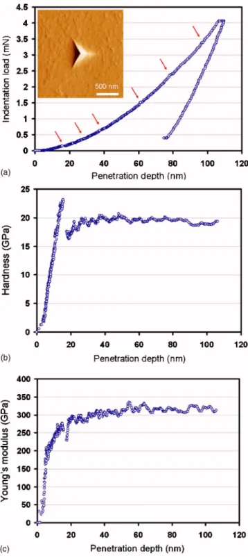
Figure1共a兲illustrates the typical nanoindentation curve
obtained for Al0.16Ga0.84N thin film. The total penetration
depth into thin film was⬃110 nm with a peak load of 4 mN.
The hardness and Young’s modulus of Al0.16Ga0.84N thin film
can be calculated from the load-displacement data by the
analytic method developed by Oliver and Pharr.9In addition,
with the continuous contact stiffness measurements, the
pen-FIG. 1.共Color online兲 Nanoindentation test results: 共a兲 a load-displacement curve of Al0.16Ga0.84N thin film showing the multiple “pop-ins” 共arrows兲 during loading. Inset: The corresponding AFM nanoindented image. 共b兲 Hardness-displacement curve and共c兲 Young’s modulus-displacement curve for Al0.16Ga0.84N thin film.
033503-2 Jian, Juang, and Lai J. Appl. Phys. 103, 033503共2008兲
etration depth dependence of the hardness and Young’s
modulus can be obtained, shown in Figs.1共b兲 and1共c兲.
It is interesting to note the load-displacement curve in Fig.1共a兲, which exhibits irregularities in the course of plastic deformation characterized by the multiple discontinuities at
certain penetration depths共see arrows兲, referred to as
“pop-ins.” This observation is in contrast to that reported in the previous studies of AlGaN thin films,5,15where only a single “pop-in” was observed. The origin of this discrepancy is not clear at present. We speculate that different operating modes may lead to the dissimilar nanoindentation results. Moreover, it is noted that the events of multiple pop-ins are coinciding nicely with sudden decreases in the hardness of measured
materials.16 As can be seen in Fig. 1共b兲, the hardness of
Al0.16Ga0.84N thin film decreases abruptly at the penetration
depth of ⬃18 nm corresponding to the first pop-in event.
The hardness after the first pop-in for Al0.16Ga0.84N thin film
remains nearly constant at 19.76⫾0.15 GPa with small
fluc-tuations, possibly associated with dislocation activities.
Similarly, as shown in Fig. 1共c兲, the Young’s modulus of
Al0.16Ga0.84N films also displays a sudden drop occurring
around the same penetration depth and then remains
rela-tively constant at 310.63⫾9.41 GPa. As is compared in
TableI, the Young’s modulus obtained in the present study is
significantly smaller than those reported by Cáceres et al.,15
albeit similar values for hardness were obtained.
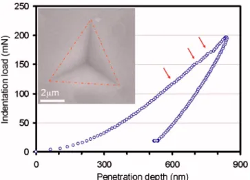
Figure2shows the similar load-displacement results
ob-tained with a much larger load of 200 mN and deeper pen-etration up to 900 nm. Although the resolution was much reduced due to larger indentation load, similar multiple pop-ins are evident. The fact that multiple pop-pop-ins are observable over such a wide range of indentation load and penetration depth indicates the close relations to the plastic deformation of the film. Furthermore, since the multiple pop-ins are
ran-domly distributed on the loading curve in Figs.1共a兲and each
curve is associated with a different stress rate, which in-creases with the maximum indentation load, it is suggestive that the first pop-in is not thermally activated. Instead, these phenomena are usually attributed to dislocation nucleation and propagation during loading, as have been observed in a wide variety of materials,17,18 or micro-cracking.19 In addi-tion, the reverse discontinuities during the unloading curve, the so-called “pop-out” event, commonly observed in silicon and attributed to pressure-induced phase transition,20,21is not observed here. Thus, it is clear that the first pop-in event may reflect the transition from perfectly elastic to plastic defor-mation, that is, it is the onset of plasticity in Al0.16Ga0.84N thin film. The corresponding shear stress under the
Berkov-ich indenter at indentation load P*, where the
load-displacement discontinuity occurs, can be determined by us-ing the followus-ing relation:22
max= 0.31
冉
6P*E2
3R2
冊
0.33, 共1兲
where R is the radius of the tip of the indenter, and E is defined in terms of Young’s moduli and Poisson’s ratios of the diamond indenter and thin film. Comparisons of our mea-surement results of mechanical properties of AlGaN thin films with those reported by previous studies are presented in TableI. Again, the large critical shear stressmaxobtained in
this study may arise from the measuring method used. Returning to the multiple pop-in behaviors displayed by the AlGaN thin films, it should be noted that similar phenom-ena have been observed previously in hexagonal structured
sapphire,23GaN thin films,24 and single-crystal bulk ZnO.25
On the other hand, materials with cubic structure such as InP
and GaAs exhibited only single pop-in characteristic.26One
possible mechanism being proposed to explain the observed behavior was the slipping systems available for the forma-tion and propagaforma-tion of dislocaforma-tions in the material. The mul-tiple slipping systems inherent to hexagonal structure mate-rials are believed to be the primary reason for the resulting multiple pop-ins phenomena. In addition, the SEM
observa-tion shown in the inset of Fig.2does not reveal any evidence
of material pile-ups and signs of crack formation on the film surface around the indented area. Since there are no multiple
“pop-outs” on the unloading curves either共Fig.2兲, this
sug-gests that phase transitions like that observed in indented Si
共Ref.20兲 probably are not occurring in the present case. The
above discussions indicate that nanoindentation-induced de-formation in Al0.16Ga0.84N thin film is predominantly due to
dislocation nucleation and propagations. This plastic defor-mation process is complex and further studies will be neces-sary to delineate what happens to the material as the indenter penetrates into the surface. The nanoindentation-induced
de-TABLE I. Mechanical properties of AlGaN thin films obtained in this study and those reported in the literature.
Samples H共GPa兲 E共GPa兲 P*共mN兲 max共GPa兲 Al0.16Ga0.84Na 19.76⫾0.15 310.63⫾9.41 0.14⫾0.02 31.01⫾0.04 Al0.12Ga0.88Nb 19.24⫾4.76 315.23⫾43.09 1.29⫾0.11 2.98⫾0.49 Al0.17Ga0.83Nc ⬃19.8 371⫾4 1.35 7.1⫾0.3 Al0.21Ga0.79Nc ⬃19.7 382⫾5 1.45 7.6⫾0.6 Al0.27Ga0.73Nc ⬃19.5 380⫾4 0.8 6.3⫾0.3 aPresent work. bReference5. cReference15.
FIG. 2. 共Color online兲 SEM micrograph 共inset兲 of a Berkovich indentation on Al0.16Ga0.84N thin film obtained at an indentation load of 200 mN and the multiple “pop-ins” also displayed in the load-displacement curve.
formation mechanisms will be discussed in more detail with the aid of XTEM techniques in the following.
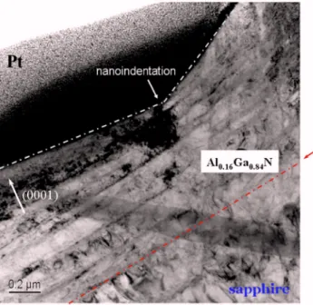
A bright-field XTEM image of Al0.16Ga0.84N thin film
after being indented with an indentation load of 200 mN is displayed in Fig. 3. It clearly displays that, within this thin film, the deformation features underneath the indented spot are primarily manifested by dislocation activities. Namely
the slip bands are aligning parallel to the兵0001其 basal planes
all the way down to the thin-film–substrate interface. It is also interesting to note that the heavily strained features in the vicinity of the interface may not be just accidental arti-facts resulting from sample preparation. It might be direct evidence for displaying that, because of the excellent inter-face epitaxy between thin film and substrate, the effects of nanoindentation have, in fact, extended into the sapphire substrate. This argument may also partially explain that, due to the ease of relaxing the local stress right under the indent-er’s tip via the massive substrate, indentation-induced phase transitions were rarely observed.
In the present study, in addition to those aligning parallel
to Al0.16Ga0.84N-sapphire interface along the 共0001兲 basal
planes, slip bands oriented at⬃60° to the sample surface can
also be found. The ⬃60° slip bands, which are believed to
originate from dislocations gliding along the兵101¯1其
pyrami-dal planes, however, are distributing in much shallower re-gions near the contacting surface. It is indicative that much higher stress level is needed to activate this slip system as compared to the one along the basal planes. The distorted slip bands and the extremely high dislocation densities at the intersections indicate a highly strained state of the material. Nevertheless, even at the submicron scale, no evidence of subsurface cracking and thin film fragmentation was
ob-served. In addition, the selected area diffraction 共not shown
here兲 of the heavily damaged regions did not show evidence of newly formed phases either.
In closing, from the above observations and discussion,
it is apparent that, in the Berkovich indentation scheme, the
primary deformation mechanism for Al0.16Ga0.84N thin film
is dislocation nucleation and propagation along easy slip sys-tems. Since the multiple pop-ins are usually observed after permanent plastic deformation has occurred and two of the
possible mechanisms, the deformation-induced phase
transition20,27 and fracture of thin films,19 were basically ruled out, the most likely mechanism responsible for the multiple pop-ins appears to be associated with the activation of dislocation sources.28In this scenario, plastic deformation prior to the pop-in event is associated with the individual movement of a small number of newly nucleated and preex-isting dislocations. As the number of dislocations is in-creased and entangled to each other, large shear stress is quickly accumulated underneath the indenter tip. When the local stress underneath the tip reaches some threshold level, a burst of collective dislocation movement on the easy slip systems is activated, leading to a large release of local stress and a pop-in event on the load-displacement curve. Each of these collective dislocation movements is reflected as a slip
band in the indented microstructure displayed in Fig.3.
No-tice that, although the slip bands appeared to stop near the thin-film–substrate interface, the released stress due to this effect could extend deep into the substrate as mentioned above. Moreover, the narrow spacing of the dense bands of defects and/or dislocations along the basal planes near the surface suggests that, in the later stage of indentation, a large indentation load, such as the 200 mN used in the present experiments, starts to activate extensive slip bands along the ⬃60° pyramidal planes. The extensive interactions between the dislocations slipping along the two slip systems, there-fore, confined the slip bands in a shallow regime, which, in turn, resulted in a heavily deformed and strain-hardened lat-tice structure. Finally, we note that the so-called “slip-stick”
behavior,29 characterized by material pile-ups caused by
in-teractions between the as-grown defects and the
nanoindentation-induced dislocations, is not significant in this study. Whether it is due to the insignificant grown-in defect density of our AlGaN films or is related to the specific geometric shape of the indenter tip used is not clear at present and further studies may be required to clarify this issue.
IV. CONCLUSION
To summarize, in this study the mechanical responses of
MOCVD Al0.16Ga0.84N thin film to nanoindentation have
been investigated by combining nanoindentation and micro-scopic techniques. Multiple “pop-ins” were observed in the load-displacement curves and appeared to occur randomly with increasing indentation load. These instabilities are at-tributed to the dislocation nucleation and propagation. No evidence of either phase transformation or formation of micro-cracking was observed by AFM, SEM, and even XTEM. The absence of nanoindentation-induced new phases might have been due to the stress relaxation via substrate and is also consistent with the fact that no discontinuity was found upon unloading. Moreover, it is noted that both the basal and pyramidal planes of Al0.16Ga0.84N lattice are acting
FIG. 3. 共Color online兲 Bright-field XTEM image of Al0.16Ga0.84N thin film subjected to an indentation load of 200 mN.
033503-4 Jian, Juang, and Lai J. Appl. Phys. 103, 033503共2008兲
as the primary slip systems for collective dislocation mo-tions, with the latter being activated at a higher stress state and hence a later stage of indentation. The hardness and
Young’s modulus of Al0.16Ga0.84N thin film estimated using
the continuous stiffness operation mode provided with the
nanoindenter are 19.76⫾0.15 and 310.63⫾9.41 GPa,
re-spectively.
ACKNOWLEDGMENTS
This work was partially supported by National Science Council of Taiwan through Grant No. NSC 96-2112-M-214-001.
1T. D. Moustakas, E. Iliopoulos, A. V. Sampath, H. M. Ng, D. Doppal-apudi, M. Misra, D. Korakakis, and R. Singh, J. Cryst. Growth 227–228, 13共2001兲.
2M. Asif Khan, M. Shatalov, H. P. Maruska, H. M. Wang, and E. Kuokstis, Jpn. J. Appl. Phys., Part 1 44, 7191共2005兲.
3D. W. Kim, K. S. Chea, Y. J. Park, I. H. Lee, and C. R. Lee, Phys. Status Solidi A 201, 2686共2004兲.
4X. D. Li, H. Gao, C. J. Murphy, and K. K. Caswell, Nano Lett. 3, 1495 共2003兲.
5S.-R. Jian, T.-H. Fang, and D.-S. Chuu, J. Electron. Mater. 32, 496共2003兲. 6X. D. Li, H. Gao, C. J. Murphy, and L. Gou, Nano Lett. 4, 1903共2004兲. 7X. D. Li, X. Wang, Q. Xiong, and P. C. Eklund, Nano Lett. 5, 1982共2005兲. 8S.-R. Jian, T.-H. Fang, and D.-S. Chuu, Appl. Surf. Sci. 252, 3033共2006兲. 9W. C. Oliver and G. M. Pharr, J. Mater. Res. 7, 1564共1992兲.
10A. Mujica, A. Rubio, A. Muñoz, and R. J. Needs, Rev. Mod. Phys. 75, 863 共2003兲.
11J. H. A. Hagelaar, E. Bitzek, C. F. J. Flipse, and P. Gumbsch, Phys. Rev. B
73, 045425共2006兲.
12Q. Tang and F. Chen, J. Phys. D 39, 3674共2006兲.
13S.-R. Jian, T.-H. Fang, D.-S. Chuu, and L.-W. Ji, Appl. Surf. Sci. 253, 833 共2006兲.
14K. Wasmer, C. Ballif, R. Gassilloud, C. Pouvreau, R. Rabe, J. Michler, J. M. Breguet, J. M. Solletti, A. Karimi, and D. Schulz, Adv. Eng. Mater. 7, 309共2005兲.
15D. Cáceres, I. Vergara, R. González, E. Monroy, F. Calle, E. Muñoz, and F. Omnès, J. Appl. Phys. 86, 6773共1999兲.
16J. E. Bradby, J. S. Williams, and M. V. Swain, J. Mater. Res. 19, 380 共2004兲.
17D. F. Bahr, D. E. Kramer, and W. W. Gerberich, Acta Mater. 46, 3605 共1998兲.
18A. J. Haq, P. R. Munroe, M. Hoffman, P. J. Martin, and A. Bendavid, Thin Solid Films 515, 1000共2006兲.
19S. J. Bull, J. Phys. D 38, R393共2005兲.
20J. E. Bradby, J. S. Williams, J. Wong-Leung, M. V. Swain, and P. Munroe, Appl. Phys. Lett. 77, 3749共2000兲.
21J. E. Bradby, J. S. Williams, J. Wong-Leung, M. V. Swain, and P. Munroe, J. Mater. Res. 16, 1500共2001兲.
22K. L. Johnson, Contact Mechanics共Cambridge U. P., Cambridge, UK, 1985兲.
23R. Nowak, T. Sekino, S. Maruno, and K. Niihara, Appl. Phys. Lett. 68, 1063共1996兲.
24S. O. Kucheyev, J. E. Bradby, J. S. Williams, C. Jagadish, M. V. Swain, and G. Li, Appl. Phys. Lett. 78, 156共2001兲.
25S. O. Kucheyev, J. E. Bradby, J. S. Williams, C. Jagadish, and M. V. Swain, Appl. Phys. Lett. 80, 956共2002兲.
26J. E. Bradby, J. S. Williams, J. Wong-Leung, M. V. Swain, and P. Munroe, Appl. Phys. Lett. 78, 3235共2001兲.
27D. J. Oliver, J. E. Bradby, J. S. Williams, M. V. Swain, and P. Munroe, J. Appl. Phys. 101, 043524共2007兲.
28Y. Gaillard, C. Tromas, and J. Woirgard, Philos. Mag. Lett. 83, 553共2003兲. 29J. E. Bradby, S. O. Kucheyev, J. S. Williams, J. Wong-Leung, M. V. Swain, P. Munroe, G. Li, and M. R. Phillips, Appl. Phys. Lett. 80, 383 共2002兲.