Discrete monolayer light emission from GaSb wetting layer in GaAs
Ming-Cheng Lo, Shyh-Jer Huang, Chien-Ping Lee, Sheng-Di Lin, and Shun-Tung Yen
Citation: Applied Physics Letters 90, 243102 (2007); doi: 10.1063/1.2748087
View online: http://dx.doi.org/10.1063/1.2748087
View Table of Contents: http://scitation.aip.org/content/aip/journal/apl/90/24?ver=pdfcov Published by the AIP Publishing
Articles you may be interested in
Atom probe tomography analysis of different modes of Sb intermixing in GaSb quantum dots and wells Appl. Phys. Lett. 103, 122102 (2013); 10.1063/1.4821549
Wetting layer states of In As Ga As self-assembled quantum dot structures: Effect of intermixing and capping layer
J. Appl. Phys. 101, 063539 (2007); 10.1063/1.2711146
Correlation between interface structure and light emission at 1.3–1.55 m of (Ga,In)(N,As) diluted nitride heterostructures on GaAs substrates
J. Vac. Sci. Technol. B 22, 2195 (2004); 10.1116/1.1775197
Blue-light emission from molecular-beam-epitaxially grown GaN/Al 0.5 Ga 0.5 N multiple quantum wells with a perturbating layer of Al 0.5 Ga 0.5 N monolayers
Appl. Phys. Lett. 84, 4478 (2004); 10.1063/1.1755836
Experimental and theoretical study of strain-induced AlGaAs/GaAs quantum dots using a self-organized GaSb island as a stressor
J. Appl. Phys. 86, 2001 (1999); 10.1063/1.371000
This article is copyrighted as indicated in the article. Reuse of AIP content is subject to the terms at: http://scitation.aip.org/termsconditions. Downloaded to IP: 140.113.38.11 On: Thu, 01 May 2014 00:25:41
Discrete monolayer light emission from GaSb wetting layer in GaAs
Ming-Cheng Lo,a兲Shyh-Jer Huang, Chien-Ping Lee, Sheng-Di Lin, and Shun-Tung Yen
Department of Electrical Engineering, National Chiao Tung University, 1001 Ta Hsueh Road, Hsin Chu 300, Taiwan, Republic of China
共Received 4 April 2007; accepted 18 May 2007; published online 11 June 2007兲
Distinct light emission peaks from monolayers of GaSb quantum wells in GaAs were observed. Discrete atomic layers of GaSb for the wetting layer prior to quantum dot formation give rise to transition peaks corresponding to quantum wells with 1, 2, and 3 ML. From the transition energies the authors were able to deduce the band offset parameter between GaSb and GaAs. By fitting the experimental data with the theoretical calculated result using an 8⫻8 k·p Burt’s Hamiltonian along with the Bir-Picus deformation potentials, the strain-free共fully strained兲 valence band discontinuity for this type-II heterojunction was determined to be 0.45 eV共0.66 eV兲. © 2007 American Institute
of Physics. 关DOI:10.1063/1.2748087兴
III-antimonide compounds have been regarded as poten-tial materials for applications in ultrahigh-speed devices and long-wavelength photonic devices due to their high electron mobility and small band gap energies.1,2 Moreover, hetero-structures composed of antimonides and other III-V com-pounds, such as arsenides, have also been of physical interest because of the unconventional type-II and type-III band alignment.3–5There have been lots of theoretical predictions for interesting optical, electronic, and magnetic phenomena in nanostructures with antimonides.6 Recently, with the ad-vances in epitaxy technology, such nanostructures have been grown with high quality and from them many interesting experimental findings, either predicted or sometimes unex-pected, have been observed. For instance, quantum wells 共QWs兲 and self-assembled quantum dots 共QDs兲 made by GaSb embedded in GaAs matrix, because of type-II hetero-structures, can provide an opportunity for observation of op-tical transition between spatially separate electrons and holes around the heterointerfaces. However, despite a large amount of effort being put in this material system, one of the most important parameters, the band offset between GaSb and GaAs has yet to be accurately determined. The wide range of reported value in this parameter often leads to ambiguous interpretation of experimental results and theoretical predic-tions for nanostructures made from this system.
In this work, we report a study on optical transitions from monolayer-scale GaSb/ GaAs QWs. Several distinct emission peaks were observed simultaneously from more than one sample by photoluminescence 共PL兲 measurement. Each of the emission peaks lies at a definite position and can be well assigned to an optical transition from the QW of 1, 2, or 3 ML. Such definite transition energies allow us to deter-mine the band offset between GaSb and GaAs by fitting the theoretical calculation to the measured data. Additionally, we also observed a subordinate emission peak that can be as-signed to the optical transition in QDs. The QD emission can be observed only from the sample with a particular nominal GaSb thickness. Our study can therefore provide an insight into the mechanism for the formation of GaSb/ GaAs QDs by molecular beam epitaxy共MBE兲.
The GaSb/ GaAs nanostructures were grown by a VECCO Gen-II solid source MBE system with valve cracker sources of antimony and arsenic on共001兲 GaAs substrates. Two samples were prepared with different nominal GaSb film thicknesses:共1兲 sample A has a 1 ML GaSb film and 共2兲 sample B has a 2 ML GaSb film. Here, 1 ML GaSb film means the number of GaSb molecules that is needed to form a continuous GaSb layer pseudomorphically matched to GaAs. In both samples, the GaSb films were sandwiched between a 150 nm GaAs buffer layer and a 150 nm GaAs capping layer. After the capping layer growth, a GaSb film with the same thickness was grown on the surface for atomic force microscope 共AFM兲 measurement. We have monitored the reflection high-energy electron diffraction patterns to make sure that the morphology of GaSb layer on the surface is the same as that buried in the sample. The growth tem-perature for GaSb was 500 ° C, the V/III flux ratio was about 5, and the growth rate was 0.2 ML/ s. After the growth of the GaAs buffer layer, the As shutter was closed, the Sb shutter was opened, and the GaSb film was immediately deposited. Following that, a 1 min interruption under Sb flux was per-formed. We used As4as the arsenic source instead of As2to
avoid intermixing of Sb and As atoms during the growth process.7
Figures1共a兲and1共b兲 show the AFM images of samples A and B, respectively. The smooth surface of sample A clearly shows that 1 ML of GaSb is not enough for quantum dot formation. However, on the surface of sample B, which had a 2 ML GaSb film, we can see clear images of quantum
a兲Electronic mail: [email protected] FIG. 1.square image area共Color online兲 AFM surface images of 共a兲 sample A 共with 5兲 and 共b兲 sample B 共with 1m square image area兲. m APPLIED PHYSICS LETTERS 90, 243102共2007兲
0003-6951/2007/90共24兲/243102/3/$23.00 90, 243102-1 © 2007 American Institute of Physics
This article is copyrighted as indicated in the article. Reuse of AIP content is subject to the terms at: http://scitation.aip.org/termsconditions. Downloaded to IP: 140.113.38.11 On: Thu, 01 May 2014 00:25:41
dots. The density of the dots is about 1.04⫻1010 cm−2 and
the height and the diameter of QDs are in the ranges of 5 – 10 nm and 50– 60 nm, respectively. The formation of dots implies that the strain of the GaSb film cannot be sustained pseudomorphically in GaAs when more than 1 ML of GaSb is deposited. This is obviously due to the large lattice mis-match共8%兲 between GaSb and GaAs. However, as will be described in the following, because of the nature of epitaxial growth, 1 ML GaSb deposition does not mean that there is only one kind of quantum wells with thickness of 1 ML. Actually what we found in this work is that the maximum thickness of GaSb wetting layer共or quantum well兲 is 3 ML. The PL measurement of the two samples was performed at 15 K with a cw Ar laser as the excitation source. The excitation power was varied from 1 to 100 mW and the beam spot size was around 200m in diameter. The mea-sured spectra of samples A and B are shown in Figs.2共a兲and
2共b兲, respectively. For sample A关see Fig.2共a兲兴, the dominant peak is A1 at⬃1.4 eV. At low excitation levels, this is the
only peak observed. However, when the excitation exceeds 100 mW, two additional peaks A2 and A3 at about 1.3 and
1.22 eV are observed along with the main peak A1. For
sample B, the situation is more complicated. From Fig.2共b兲, one can see that the emission is dominated by the peak B2at
⬃1.3 eV at all excitation levels. With the excitation level increasing, the side peaks B1 and B3, at 1.22 and 1.4 eV,
respectively, become more obvious. It is noticed that the three peaks Bifor sample B appear exactly at the same
po-sitions of the peaks Aifor sample A共i=1,2,3兲. At the
exci-tation of 100 mW, we also found a broad peak BQDaround
1.05 eV in the spectrum for sample B. This peak is absent from the spectra for sample A and should be attributed to optical transition in QDs.
The fact that the positions of the emission peaks from two different samples are identical indicates that they origi-nate from optical transitions in QWs with the same ness. The fact that the QW in sample A has a nominal thick-ness of 1 ML allows us to assign the main peak A1 to the optical transition in 1 ML QWs. Consequently, the lower peaks A2and A3at lower energies can be assigned to optical
transitions in 2 and 3 ML QWs, respectively. As will be seen later, this assignment is in reasonable agreement with our calculation result. Based on a similar argument, the main peak B2 of sample B, which was deposited with 2 ML of
GaSb, is due to the optical transition in 2 ML QWs. The two side peaks B1 and B3, therefore, naturally come from optical
transitions in 1 and 3 ML QWs, respectively. The emission peak from the quantum dots BQD is obviously wider than
those from the quantum wells. This is caused by the nonuni-formity in the size of the QDs. In contrast, the emission peaks from the thin QWs are narrower. The discreteness of the atomic layers in these monolayer QWs gives no contri-butions to the linewidth broadening due to thickness fluctua-tions, which is normally seen in wide QWs.
The emission spectra described above have revealed that thin QWs with different number of atomic layers can coexist when a few monolayers of GaSb are deposited in GaAs. Such peculiar emission spectra have not been seen in the more popular InAs/ GaAs system. The InAs wetting layer prior to the quantum dot formation usually shows only one broad emission peak. While it is unlikely that the thin InAs layer is atomically smooth without steps, the single emission peak is probably due to an average effect of the transition
energy caused by some kind of intermixing between the In and the Ga atoms after the quantum dot formation. On the other hand, the coexistence of 1, 2, and 3 ML QWs in the GaSb films indicates that the morphological pattern with atomic steps remains intact after they are covered with GaAs. In this work, we used As4 instead of As2 as the arsenic
source for GaAs growth, which may have contributed to the reduction in intermixing between As and Sb.7
Because of the spatial separation between electrons and holes in the type-II GaSb/ GaAs heterostructures, the carrier recombination lifetime is long and the carrier density can significantly increase with the excitation power. It follows that the electric field, which is induced by the spatially sepa-rated electron-hole space charges, increases around the het-erointerface with the excitation power. As illustrated in the inset of Fig.3, the increased electric field causes an upward shift of the energy level in the triangular potential well on the GaAs side. The observed blueshift for the emission peaks from GaSb/ GaAs heterostructures is usually proportional to the 1 / 3 power of the excitation level, which is consistent with the triangular well approximation for electrons in GaAs.2,3Figure3shows the energy positions of the emission peaks A1and B2as functions of the cubic root of the excita-tion power density. The upper and lower lines in the figure, corresponding to A1and B2, respectively, show how the
tran-sition energies in the 1 and 2 ML QWs change with excita-tion power. As seen in the figure, the energy shift follows the 1 / 3 power dependence quite well. However, it should be FIG. 2. Photoluminescence spectra of共a兲 sample A and 共b兲 sample B at 15 K.
FIG. 3. Measured transition energy vs the cubic root of the excitation power. The interceptions of the extrapolated lines with the y axis give the transition energies at thermal equilibrium. The carrier transition diagram for a GaSb/ GaAs quantum well is shown in the inset.
243102-2 Lo et al. Appl. Phys. Lett. 90, 243102共2007兲
This article is copyrighted as indicated in the article. Reuse of AIP content is subject to the terms at: http://scitation.aip.org/termsconditions. Downloaded to IP: 140.113.38.11 On: Thu, 01 May 2014 00:25:41
noted that the excitation power was kept below 10 mW in this plot. At high pumping powers, because of local heating, the 1 / 3 power law dependence will no longer be valid.
The plot in Fig. 3 can be used to obtain the transition energies of 1 and 2 ML GaSb/ GaAs QWs in the absence of the excitation by linear extrapolation of the lines to the y axis. The obtained transition energy can be considered as the band gap energy of GaSb/ GaAs QWs at thermal equilib-rium. The resulting band gap energy is 1.404 eV for 1 ML QW and 1.298 eV for 2 ML QW. For the 3 ML QW, we cannot adopt the extrapolation method described above since we lack a series of appreciable emission signals at low exci-tation levels. Instead, we estimate the band gap energy at thermal equilibrium for the 3 ML QW to be about the posi-tion in energy of the peak B3 obtained from sample B at
excitation of 70 mW. This may overestimate the band gap energy according to the band filling effect mentioned above, but because the heating effect can compensate part of the energy shift, we expect the error is reasonably small com-pared to the difference from the band gap energy of 1 or 2 ML QW.
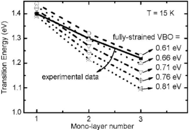
Now that the band gap energies of 1, 2, and 3 ML QWs have been obtained by the experiment, we can determine the band offset between GaSb and GaAs by fitting the theoreti-cally calculated band gap to the experimentally obtained data with the band offset as an adjusting parameter. To this end, we use the eight-band k · p model to calculate the valence band structures of GaSb/ GaAs QW in the flatband approxi-mation for various values of band offset.8The strain effect is considered, assuming the GaSb is pseudomorphically grown on strain-free GaAs, using the Bir-Picus deformation poten-tial theory. The parameters taken for calculation can be found in Ref.9. The calculated transition energy is then the differ-ence between the GaAs conduction band edge and the first heavy-hole subband edge in the GaSb QW. Figure4 shows the calculated transition energy of 1, 2, and 3 ML GaSb QWs for a series of valence band offset共VBO兲 values, along with the data obtained from measurement, where VBO is the dif-ference in valence band edge between fully strained GaSb and strain-free GaAs. As can be seen, the variation of the
transition energy with the QW thickness is quite consistent between the calculation and the measurement, proving the correctness of our previous assignment of the emission peaks to optical transition in QWs with definite monolayer-scale thickness. Comparison between the calculated and the mea-sured data suggests that the VBO should lie in the range of 0.61– 0.81 eV. The strain-free VBO should lie in the range of 0.4– 0.6 eV. For the best fitting, the fully strained VBO is 0.66 eV and the strain-free VBO is 0.45 eV. The slight de-viation in the calculated data is attributed to the emission of band bending in our calculation, which is particularly impor-tant to the structure with the 3 ML QW. There is a wide range of VBO values共from 0.12 to 0.9 eV兲 reported in the past.10–13 Our study has narrowed significantly the VBO range. Previously, Ledentsov et al. have compared the mea-sured transition energies of thin GaSb layers with their the-oretical calculations, and found a large discrepancy.3This is most likely due to a choice of a large VBO.
In conclusion, we have observed distinct PL peaks from monolayer GaSb layers in GaAs. Such peaks have been iden-tified to be originated from optical transitions in 1, 2, and 3 ML GaSb/ GaAs type-II QWs. The observed phenomenon is peculiar to the monolayer-scale GaSb/ GaAs layers and has never been found in the more popular InAs/ GaAs structures. A range of valence band offset for the strain-free GaSb/ GaAs heterojunction from 0.4 to 0.6 eV is suggested according to the fitting of the measured data to our eight-band k · p calculation.
This work was supported by the National Science Coun-cil under Contract Nos. NSC95-2221-E-009-288 and NSC95-2120-M-009-009.
1Yasuhiro Oda, Haruki Yokoyama, Kenji Kurishima, Takashi Kobayashi,
Noriyuki Watanabe, and Masahiro Uchida, Appl. Phys. Lett. 87, 023503 共2005兲.
2Q. Yang, C. Manz, W. Bronner, Ch. Mann, L. Kirste, K. Kohler, and J.
Wanger, Appl. Phys. Lett. 86, 131107共2005兲.
3N. N. Ledentsov, J. Bohrer, M. Beer, F. Heinrichsdorff, M. Grundmann,
D. Bimberg, S. V. Ivanov, B. Ya. Meltser, S. V. Shaposhnikov, I. N. Yassievich, N. N. Faleev, P. S. Kop’ev, and Zh. I. Alferov, Phys. Rev. B
52, 14058共1995兲.
4F. Hatami, N. N. Ledentsov, M. Grundmann, J. Böhrer, F. Heinrichsdorff,
M. Beer, D. Bimberg, S. S. Ruvimov, P. Werner, U. Gösele, J. Hexdenreich, U. Richter, S. V. Ivanov, B. Ya. Meltser, P. S. Kop’ev, and Zh. I. Alferov, Appl. Phys. Lett. 67, 656共1995兲.
5C.-K. Sun, G. Wang, J. E. Bowers, B. Brar, H.-R. Blank, H. Kroemer, and
M. H. Pilkuhn, Appl. Phys. Lett. 68, 1543共1996兲.
6M. Hayne, J. Maes, S. Bersier, M. Henini, L. Muller-Kirsch, Rober Heitz,
D. Bimberg, and V. V. Moshchalkov, Physica B 346-347, 421共2004兲.
7Makoto Kudo, Tomoyoshi Mishima, Satoshi Iwamoto, Toshihiro Nakaoka,
and Yasuhiko Arakawa, Physica E共Amsterdam兲 21, 275 共2004兲.
8A. Zakharova, S. T. Yen, and K. A. Chao, Phys. Rev. B 66, 085312
共2002兲.
9I. Vurgaftman, J. R. Meyer, and L. R. Ram-Mohan, J. Appl. Phys. 89,
5815共2001兲.
10A. D. Katnani and G. Margaritondo, J. Appl. Phys. 54, 2522共1983兲. 11J. Tersoff, Phys. Rev. B 30, 4874共1984兲.
12Y. Tsou, A. Ichii, and Elsa M. Garmire, IEEE J. Quantum Electron. 28,
1261共1992兲.
13F. L. Schuermeyer, P. Cook, E. Martinez, and J. Tantillo, Appl. Phys. Lett.
55, 1877共1989兲.
FIG. 4. Transition energies of quantum wells with 1, 2, and 3 ML of GaSb. The measured result is compared with the theoretical result.
243102-3 Lo et al. Appl. Phys. Lett. 90, 243102共2007兲
This article is copyrighted as indicated in the article. Reuse of AIP content is subject to the terms at: http://scitation.aip.org/termsconditions. Downloaded to IP: 140.113.38.11 On: Thu, 01 May 2014 00:25:41