國
立
交
通
大
學
資訊科學與工程研究所
碩
士
論
文
非同步雙道超大指令字組處理器之
預解碼迴圈緩衝器設計
Predecode Loop Buffer Design for Asynchronous two-way VLIW
Processor
研 究 生:陳建志
非同步雙道超大指令字組處理器之預解碼迴圈緩衝器設計
Predecode Loop Buffer Design for Asynchronous two-way VLIW Processor
研 究 生:陳建志 Student:Jian-Jhih Chen
指導教授:陳昌居 Advisor:Chang-Jiu Chen
國 立 交 通 大 學
資 訊 科 學 與 工 程 研 究 所
碩 士 論 文
A ThesisSubmitted to Institute of Computer Science and Engineering College of Computer Science
National Chiao Tung University in partial Fulfillment of the Requirements
for the Degree of Master
in
Computer Science
September 2010
Hsinchu, Taiwan, Republic of China
非同步雙道超大指令字組處理器之預解碼迴圈
緩衝器設計
研究生:陳建志
指導教授:陳昌居 教授
國立交通大學資訊科學與工程研究所
摘 要
現今處理器採用的電路多為同步電路,也就是由時脈驅動的電路。時脈會造 成時脈偏差的問題,非同步電路是一種沒有時脈的電路,所以非同步電路設計可 以避免時脈產生的時脈偏差問題。迴圈緩衝器設計在現今的數位訊號處理器或者 嵌入式處理器中,是一個非常普遍且實用的元件。迴圈緩衝器不僅能減少指令記 憶體的存取次數,更能達到增進效能。 然而,傳統的迴圈緩衝器中的迴圈偵測機制,卻往往造成一個經常執行的指 令被執行頻率不高的指令替換因此本篇論文設計了一個新穎的迴圈偵測機制,不 僅能避免執行頻率高的迴圈被替換,更能減少指令解碼單元部分運算。 我們將預解碼迴圈緩衝器實現在一款無時脈的非同步雙道超大指令字組處 理器。 我們使用 Design Compiler 合成,預解碼迴圈緩衝器合成所產生的結果 為面積 240000μm2 、延遲 7.41 ns.ii
Predecode Loop Buffer Design for Asynchronous
two-way VLIW Processor
Student:Jian-Jhih Chen
Advisor:Dr. Chang-Jiu Chen
Institute of Computer Science and Engineering College of Computer Science
National Chiao Tung University
Abstract
Most modern processors are synchronous circuit that is triggered by clock. Clock would produce the problem that is clock skew. Asynchronous circuit is clockless and the problem of clock skew it can be avoided by handshake protocol. Loop buffer design is a common and useful unit for modern digital signal processors or embedded processors. It is not only could decrease the access times of instruction memory, but could improve performance.
However, traditional loop buffers always let the frequently executed instruction be replaced by another infrequently executed instruction. Thus, this thesis designs a novel loop detection that could avoid a frequently executed instruction be replaced and reduce the operations of instruction fetch and decode.
Predecode Loop Buffer will be implemented on asynchronous two-way VLIW processor. Predecode Loop Buffer is synthesized by Design Compiler. Its area is about
Acknowledgement
完成這篇論文,首先要感謝我的指導教授 – 陳昌居教授,感謝老師提供良好的 研究環境與設備,以及這兩年在研究方面給了很多想法以及建議的鄭緯民博士、 張元騰學長以及蔡宏岳學長,最後謝謝李國成,張瑞宏,鄒柏成,三位同學努力 不懈的與我一起討論以及研究。
iv
CONTENTS
摘 要 ... i ABSTRACT ... ii ACKNOWLEDGMENT ... iii CONTENTS ... iv LIST OF FIGTURES ... viLIST OF TABLES ... viii
CHAPTER 1. INTRODUCTION ... 1
1.1 Motivation ... 2
1.2 The Organization of the thesis ... 3
CHAPTER 2. RELATED WORKS... 4
2.1 Asynchronous circuits ... 4
2.1.1 Advantages and drawbacks ... 5
2.1.2 4-Phase Handshake Protocol ... 7
2.1.3 Dual Rail Data Encoding Methods ... 9
2.2 Asynchronous pipeline ... 11
2.2.1 Muller C-element ... 12
2.2.2 Complete Detection... 13
2.2.3 4-Phase Dual-Rail Pipeline ... 14
2.3 Loop Detection ... 16
2.3.1 Counter-Based Loop Detection ... 16
2.3.1 Basic Block Loop Detection ... 18
2.4 Decoded Filter Cache ... 21
CHAPTER 3. THE DESIGN OF PREDECODE LOOP BUFFER ... 23
3.1.1 Pipeline Architecture ... 23
3.1. 2 Branch Instruction ... 26
3.2 Predecode Loop Buffer ... 29
3.2.1 Overview ... 32
3.2.2 Branch Information Table ... 34
3.2.3 Mode Controller ... 37
3.2.4 Procedure of Predecode Loop Buffer... 40
3.2.5 Miss Recovery Mechanism ... 46
CHAPTER 4. SIMULATION RESULT ... 48
4.1 Area Simulation ... 48
4.2 Timing Simulation ... 49
CHAPTER 5. CONCLUSIONS AND FUTURE WORKS ... 51
vi
LIST OF PICTURES
Fig 2-1 Bundled Data Channel ... 8
Fig 2-2 Four-Phase Handshake Protocol ... 8
Fig 2-3 Diagram of Dual-Rail Data Encoding ... 10
Fig 2-4 4-Phase Dual-Rail Handshake Protocol ... 10
Fig 2-5 Transfer Diagram ... 11
Fig 2-6 Muller C-element and its RTL Implementation ... 12
Fig 2-7 Muller C-element and its RTL Implementation with Reset ... 13
Fig 2-8 3-bits Alternative Complete Detection ... 13
Fig 2-9 Four-Phase Bundled Data Pipeline ... 14
Fig 2-10 Four-Phase Bundled Data Pipeline with Function Blocks ... 14
Fig 2-11 Four-Phase Dual-Rail Data Pipeline ... 14
Fig 2-12 Short Backward Branch Instruction ... 17
Fig 2-13 Count Based Scheme to Monitor Sbb Executions ... 17
Fig 2-14 Basic Blocks in Instruction Stream ... 19
Fig 2-15 Processor Pipeline with Decode Filter Cache... 22
Fig 3-1 The Pipeline Architecture of Asynchronous Two Way Processor ... 24
Fig 3-2 C_Latch ... 26
Fig 3-4 Branch Handling Architecture ... 27
Fig 3-5 The Combination of Valid Token and Empty Token ... 28
Fig 3-6 The Example of Program ... 30
Fig 3-7 The Block Diagram of Instruction Decode Stage ... 31
Fig 3-8 The Architecture of Predecode Loop Buffer ... 32
Fig 3-9 The DeMux and Merge ... 33
Fig 3-10 The Branch Information Table ... 34
Fig 3-11 The Mutual Exclusion ... 35
Fig 3-12 BIT Block Diagram ... 36
Fig 3-13 The Possible Transition of Mode ... 37
Fig 3-14 The Transition Phase and Program Phase ... 39
Fig 3-15 The Block Diagram of Mode Controller ... 40
Fig 3-16 A Frequent Loop in a Program ... 41
Fig 3-17 The Case of Instruction... 43
Fig 3-18 The Hardware Solves the Instruction with Same Address ... 43
Fig 3-19 Miss Recovery Mechanism ... 47
viii
LIST OF TABLES
Table 2-1 Dual-Rail Encoding Method... 9
Table 2-2 Truth Table of Muller C-element ... 11
Table 2-3 Power Dissipation in StrongARM ... 21
Table 3-1 The Transition Events of Mode ... 38
Table 3-2 The Relation between P-Bit and Change Bit ... 45
Table 3-3 The Relation between Change Bit and Index ... 45
Table 4-1 The Area of Basic Element in our Predecode Loop Buffer ... 48
Table 4-2 The Area Compares with Asynchronous Two Way VLIW Processor ... 48
Chapter 1 Introduction
In recent years, asynchronous circuit design becomes more and more popular.
Synchronous circuit has a serious problem, so it will become more difficult to design circuit.
The problem is clock skew that may become more and more serious, because the clock
frequency will be too high in future. Asynchronous circuit design is clockless circuit. In other
words, asynchronous circuit does not have clock and it can avoid the clock skew. Because
asynchronous circuit does not have clock, the modules of asynchronous circuit can work only
when the modules are needed to operate. Thus it has the potential for low power consumption.
However, the accessed times of memory would affect the performance of system. If the
accessed times of memory is too much, the performance will be obviously degraded. To
reduce the accessed times of memory, many architecture approaches try to take program
behavior into consideration. A lot of embedded applications are characterized by spending a
large fraction of execution time on program loops [1] [9]. In order to execute the loops, the
same operations will be repeated again and again, including instruction fetch and instruction
decode. In fact, the accessed times of instruction memory are usually more than the accessed
times of data memory. If we can reduce the accessed times of instruction memory, the
performance will may be improved.
Loop buffer is a common component to reduce the instruction memory accessed times,
2
executed times of loop is usually decided in the run-time, the software-based only deal with
that the executed times of loop is already decided in compiler time. Thus, the hardware-based
loop buffer is better than the software-based loop buffer.
.In this thesis, we propose a loop buffer to keep the more frequent loop and promise the
frequent loop that would not be replaced by other infrequent loops. The control signals of the
instructions are stored in the loop buffer and they can reduce same actions in fetch and decode
stages. We applied it on an asynchronous two-way VLIW processor and implement it with
Verilog HDL (hardware description language).
1.1 Motivation
The power consumption of instruction fetch from memory and decode instruction to
control signal is a critical issue in VLIW processor. Most programs have many loops that
composed of the non-branch instruction and the branch instruction. These loops have the
characteristic of temporal and spatial locality, so we could try to use the characteristic to
reduce unnecessary repeated operations of fetch and decode of loops. Finally, we designed our
loop buffer and implemented it on asynchronous dual-rail two-way VLIW processor.
1.2 The Organization of the Thesis
processor. The design uses an approach to select basic blocks for placement in the loop buffer.
The rest of the thesis is organized as follows. In chapter 2, the background of asynchronous
circuits and related works of loop buffer will be discussed. In chapter 3, we present the design
and implement of our asynchronous loop buffer. In chapter 4, the simulation result will be
4
Chapter 2 Related Works
This chapter will give introduction of asynchronous circuits, and discuss basic concept of
basic blocks about loop buffer. We will show the advantages, handshake protocol and data
encoding methods in chapter 2.1. Then we will introduce the Muller pipeline, C-element and
Complete Detection in chapter 2.2. In chapter 2.3, we will descript the two ways of loop
detection to implement the loop buffer: Count-Based Loop Detection [1][2] and Basic Blocks
Loop Detection [3]. We will explain why the problem will be produced by these loop
detections. Finally, we will introduce a method to reduce decode operations by caching
decoded instructions, Decoded Filter Cache [4].
2.1 Asynchronous circuits
Asynchronous circuits design is a circuit design methodology. It is practically different
from synchronous circuit. The major difference in the two ways of circuit design is clock.
Asynchronous circuit design is clockless circuit. In other words, the asynchronous circuit
works only when necessary; thus it has the potential for low power consumption. However, it
also has many advantages. It is quite difficult to design the asynchronous circuit by the two
reasons. First, asynchronous handshake protocol is more complex than synchronous. Second,
it has few CAD tool for asynchronous circuits design than synchronous, and it makes
2.1.1 Advantages and drawbacks
Comparing with the synchronous circuit design, the asynchronous circuit design has
no global clock and uses the handshake protocol between the individual module to
perform synchronizations and communications. Based on these conceptions,
asynchronous circuits design has many advantages over synchronous counterparts. The
followings are advantages of the asynchronous circuit design:
(1)No clock skew and clock distribution problem: Clock is an important role on
communication between synchronous modules. However, clock would produce a
serious trouble about clock skew. In addition, because systems will become larger and
larger, transferring clock signals will become more and more difficult than now.
Fortunately, because it is clockless, asynchronous circuits design does not need to
consider clock skew and clock distribution problem. Asynchronous circuit design
could deal with these problems by handshake protocols.
(2)Better modularity: As different sub-circuit of synchronous circuits operate at own
clock frequency, it is a difficult job to integrate these sub-circuits into a system.
Because asynchronous circuit design uses handshake protocols to replace the global
clock, designers only need to take care of the handshake protocols on how to
communicate and synchronize between the different modules. Designers do not need
6
(3)Low power consumption: Because of no clock signals, the asynchronous circuit
design does not provide extra power to generate clock tree. The individual modules
are demand-driven in asynchronous circuits design, but the individual modules in
synchronous circuit are clock driven. This means the modules in asynchronous
systems are active only when they needed, and they do not consume any extra power
for standby. It also means that asynchronous circuits design is no clock tree.
(4)Average-case performance: In synchronous circuits system, the slowest component
would decide the maximum speed of whole system. Even though it is infrequent to
operate, it is worst-case performance. The elasticity of asynchronous circuits design
has led to the outcome that an asynchronous circuit can perform average-case.
Because each asynchronous module and completes its own itself computations and
works, the data can be send immediately to the receiver. For this factor, asynchronous
circuits design can obviously accomplish average-case performance.
(5)Less electro-magnetic noises: Asynchronous circuit design has no clock distribution
networks, so it has less electro-magnetic noises.
Although asynchronous circuit design that compares with synchronous circuits
design has many advantages, it also has some disadvantages. One is few CAD tools to
support for designers so that designers are hard to implement the circuit. Another one is
of additional control signals. Asynchronous circuit design has many advantages and few
disadvantages. But comparing with advantages and disadvantages, asynchronous circuits
design still is good for designers to implement circuits.
2.1.2 4-Phase Handshake Protocol
Each module of asynchronous circuit communicates with other modules via
handshake protocols. In general, there are two parts in asynchronous circuits design. The
two parts are data signaling and control signaling. We can define these parts below: Control Signaling: 2-phase, 4-phase etc.
Data Signaling: 1-of-n encoding, dual-rail, bundled-data etc.
The data signaling has its own communicated method to transfer data between
sender and receiver. The bundled channel which data use Boolean levels to encode
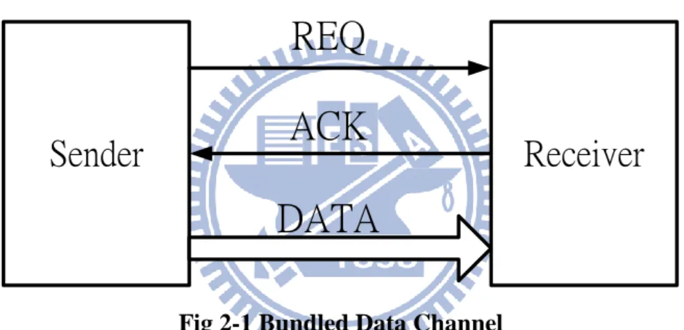
information and separates request and acknowledge wires are bundled with the data
signal. The bundled data is also called single-rail data. The bundled data channel is
shown in Fig 2-1.
Four-phase bundled data handshake protocol is shown in Fig 2-2. It uses the ACK
and REQ signal to synchronize between receiver and sender. Four-phase protocol must
return to zero after a transmission success, so it also is known as the return-to-zero
8
is asserted to 1 by Sender. When Receiver accepts the REQ signal that is 1, Receiver
knows the data is valid and receive the data. Then, Receiver will assert ACK to 1 when
the data are already received. When Sender receives the ACK equal to 1 from Receiver,
it knows the data have already transmitted to Receiver. Sender will pulls down REQ
signal to 0 and stops transferring data. Finally, the Receiver also pulls down ACK to 0.
The transfer is finished.
Sender
Receiver
REQ
DATA
ACK
Fig 2-1 Bundled Data Channel
DATA
ACK
REQ
Fig 2-2 Four-Phase Handshake Protocol
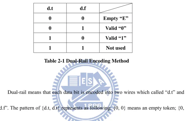
2.1.3 Dual-Rail Data Encoding Methods
point that the system does not have REQ signal, and uses 2-bit to encode 1-bit data. The
dual-rail encoding method is different from bundled data. The encoding method is shown
in Table 2-1. d.t d.f 0 0 Empty “E” 0 1 Valid “0” 1 0 Valid “1” 1 1 Not used Table 2-1 Dual-Rail Encoding Method
Dual-rail means that each data bit is encoded into two wires which called “d.t” and “d.f”. The pattern of {d.t, d.t} represents as following: {0, 0} means an empty token; {0, 1} means a valid data “0”; {1, 0} means a valid data “1”; {1, 1} means an invalid data and are not used. If the system uses dual-rail protocol to transfer n-bits data, there will
have 2xn data lines. In addition, the system does not have REQ signal, the receiver needs
an extra circuit to detect the arrival of the data signal. This special circuit is called
complete detection in dual-rail system. Fig 2-3 is a diagram of dual-rail data encoding
10
Sender
Receiver
DATA
ACK
2xn
Fig 2-3 Diagram of Dual-Rail Data Encoding
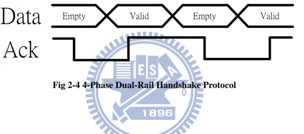
Ack
Data
Empty Valid Empty ValidFig 2-4 4-Phase Dual-Rail Handshake Protocol
Fig 2-4 shows the process of data transferring using 4-phase dual-rail protocol.
Initially, data is Empty, and it means that the data are all 0 and Ack signal is 0.When data
become valid and Receiver use complete detection to detect the data is ready, Receiver
capture data and pulls up Ack signal to 1. Then sender stops sending data and data
changes to Empty. Finally, Receiver pulls down Ack and the transfer is finished.
Dual-rail protocol uses Empty to separate each Valid data. After the transfer is completed,
the data wires will return to Empty. Thus, the sequence of data transfer is
modules based on dual-rail data encoding that is delay-insensitive, it works correctly
regardless of the delays in gates and wires.
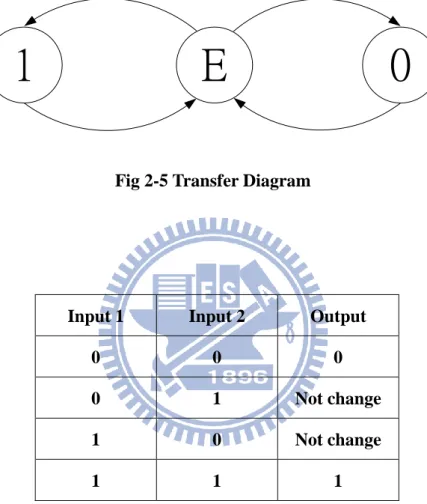
E
0
1
Fig 2-5 Transfer Diagram
Input 1 Input 2 Output
0 0 0
0 1 Not change 1 0 Not change
1 1 1
Table 2-2 Truth Table of Muller C-element
2.2 Asynchronous pipeline
There are several asynchronous pipeline implementation styles have been proposed.
Muller pipeline is one of the most important models in asynchronous pipeline. Muller pipeline
12
Muller C-element. Usually, we use the Muller C-element to control asynchronous pipeline
and implement complete detection. In this section, we introduce basic components of
asynchronous dual-rail pipeline.
2.2.1 Muller C-element
Muller C-element plays an important role on asynchronous circuit. It is a
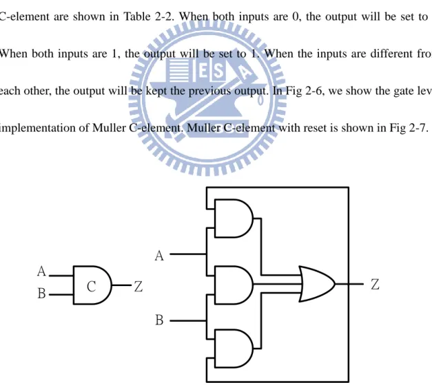
state-holding element just like an asynchronous set-reset latch. The behaviors of Muller
C-element are shown in Table 2-2. When both inputs are 0, the output will be set to 0.
When both inputs are 1, the output will be set to 1. When the inputs are different from
each other, the output will be kept the previous output. In Fig 2-6, we show the gate level
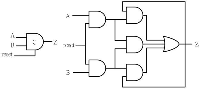
implementation of Muller C-element. Muller C-element with reset is shown in Fig 2-7.
A
A
B
B
C
Z
Z
A
B
Z
reset
A
B
C
Z
reset
Fig 2-7 Muller C-element and its RTL Implementation with Reset
2.2.2 Complete Detection
The valid data in dual-rail data encoding implementation is detected by complete
detection. If complete detection has too many inputs, a lots of C-elements are needed in
complete detection implementation. It also means very big overhead in design. In order
to reduce the overhead, we choose the alternative complete detection. The 3-bits
alternative complete detection is shown in Fig 2-8. d.t[0] d.f[0] d.t[1] d.f[1] d.t[2] d.f[2] Ackout C
14
2.2.3 4-Phase Dual-Rail Pipeline
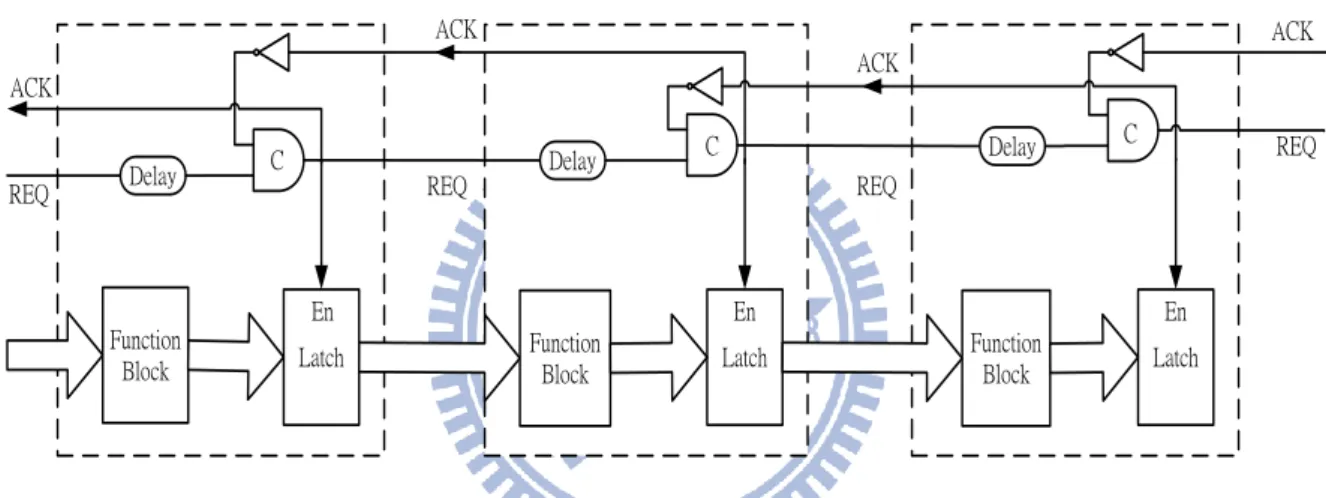
As mention above, Muller pipeline is a very popular implementation style in
asynchronous circuits design. We can use bundled data or dual-rail data based on Muller
pipeline to create design that we want. Bundled data Muller pipeline is shown in Fig 2-9.
A Muller pipeline would generate local clock pulses that just like clock of synchronous
circuits. Every stage will generate an ACK signal to previous stage and a REQ signal to
next stage. A four-phase bundle data pipeline with function blocks is shown in Fig 2-10.
If a pipeline with data processing, the combinational circuits can be added between the
stages. In order to maintain correct behaviors of every stage, matching delay must be
inserted in the request signal paths.
Another encoding way to implement Muller pipeline is dual-rail encoding method.
Because dual-rail circuit does not have the REQ signal, we must detect the data that is
already valid or not. We use the detection to decide the ACK whether pulls down or up.
The four-phase dual-rail data pipeline must alternatively send the empty token and valid
LEFT RIGHT REQ ACK REQ REQ REQ ACK ACK
C[i-1] C[i] C[i+1]
C C C
… …
ACK
Fig 2-9 Four-Phase Bundled Data Pipeline
C
Latch Latch Latch
En En En
REQ REQ REQ
ACK ACK ACK ACK REQ Function Block Function Block Function Block Delay Delay Delay C C
Fig 2-10 Four-Phase Bundled Data Pipeline with Function Block
C ACK ACK ACK ACK C C C C C C C C C C C C C C a.t a.f b.t b.t
16
2.3 Loop Detection
As mention previously, we could use the characteristic of loops in embedded systems.
These loops are small and frequently executed. It is widely known that loops have the
temporal and spatial locality. In other words, the same instructions of a loop would be
repeatedly accessed in the certain period of program execution. Often the certain period of
program execution is finished, the loop may be accessed infrequent or never be accessed
again. Thus, we must determine if the current loop should be placed into the loop buffer. As
soon as the loop becomes hot, we should place it into the loop buffer. We can use the
instructions of loop buffer to reduce the operations in instruction fetch and decoded stage,
because the instructions of frequent loops are already put in the buffer. Thus, repeated
instruction fetch and decode operations can be avoided. Otherwise, if the instructions of loop
buffer are not accessed often when the loop is detected, the instructions of the loop in the loop
buffer should be replaced. In this section, we will introduce two basic methods to decide
whether the loop should be placed into the buffer, and we also explain why the two methods
would bring some problems.
2.3.1 Counter-Based Loop Detection
The first method is counter-based loop detection [1]. The method takes advantage of the loops that may have a backward branch instruction. This characteristic is based on a special class of branch instructions, called the short backward branch instruction (sbb).
Short backward branch instruction is shown in Fig 2-12.
Because it is based on short backward branch instruction, the upper displacements
are all ones (indicating a negative branch displacement). The lower portion of
displacement is w-bits wide. By definition, a sbb has a maximum backward branch
distance given by
2
w instructions. The size of loop buffer is also given by2
winstructions. When a sbb instruction is detected and found to be taken, the hardware
assumes that a program is executing a loop and initiates all the suitable control actions to
utilize the loop buffer. The sbb is called the triggering sbb.
opcode 111…111 xx...xx
upper displacement lower displacement w bits Branch displacement
Fig 2-12 Short Backward Branch Instruction
Count_Register +1 Comparator 0 Increment Counter Triggering_sbb count w w w w / / / /
18
Counter-based scheme to monitor sbb executions is shown in Fig 2-13. When a sbb
is encountered and taken, its lower displacement is load into a w-bit increment counter
called Count_Register. The sbb becomes the triggering sbb, and the loop buffer
controller enters FILL state. In this state, the instructions that being fetched from
instruction cache fill into the loop buffer by controller. The hardware increases this
negative displacement by one, each time an instruction is executed sequentially. As the
negative value in the Count_Register increases and becomes zero, the controller knows
that the instruction currently being executed is the triggering sbb. If the triggering sbb is
not taken, controller returns to the IDLE state. Otherwise, it enters the ACTIVE state. In
the ACTIVE state, the instructions that originally request to the instruction cache would
be directed to the loop buffer by the controller.
Although the method only increases a little overheads and it is very simple, it also
have some critical problems. First, the loop that has a triggering sbb cannot have any
nested loop. Second, the loop just taken one time, and the instructions of the loop would
be putted into loop buffer. Thus, a frequently executed loop might be replacement by a
loop that just taken. Third, the loop buffer only stores the instructions of a loop, the other
unused space of loop buffer is wasted.
2.3.2 Basic Block Loop Detection
counter-based loop detection, this way is more flexible and simple. Basic block loop
detection regards a program is composed of many basic blocks. The basic block is a
straight-line code sequence composed of non-branch instructions and one branch
instruction, which determines the direction of the following instruction stream. The basic
block in program is shown in Fig 2-14.
Non-branch instrucitons Branch instruction Basic block 1: Basic block 2: Basic block 3: Non-branch instrucitons Branch instruction Non-branch instrucitons Branch instruction PBAR SC
Fig 2-14 Basic Blocks in Instruction Stream
20
would jump to a non-branch instruction when those branch instructions taken.
Basic block loop detection could be described as follows:
(1) When a branch instruction is fetched, the hardware would compare the address
of current branch instruction with the value of Previous Branch Address Register
(PBAR). If the two values are equal to each other, it means that the loop was executed
because the same branch instruction is fetched again. Thus, if two values match and the
current branch instruction is predicted as a taken branch, same instruction within the loop
will be fetched again. At the same time, these instructions are transfer to the loop buffer.
Otherwise, if the two values mismatch, it means that a new basic block will be
executed. In this status, the PBAR would store the address of current branch instruction
and reset the value in Size Counter (SC).
(2) When a non-branch instruction is fetched, the value in Size Counter would be
increased by 1. Until a branch instruction is encountered, Size Counter always is added
one because of fetching non-branch instruction. Thus, the number of instructions of the
previously executed loop could be got from Size Counter.
However, this way also has some troubles. Comparing with the counter-based loop
detection, basic block loop detection does not check the displacement of branch
instruction. It can reduce some overheads in hardware, but it is also the major problem in
by an infrequent loop. In other word, the frequent loop must be fetched and transferred
into loop buffer again, because it is replaced by an infrequent loop.
2.4 Decoded Filter Cache
In synchronous embedded processors, instruction fetch and decode unit usually take a
large percentage of total power dissipation of embedded processor [5] [6]. For example,
StrongARM spends more than 40% in instruction fetch and decode [5] [6]. The power
dissipation by different components of StrongARM is shown in Table 2-3. However, we could
take advantages of loop buffer to reduce the power consumption of instruction fetch [4]. The
decode unit still repeatedly executes the same instruction of the frequent loop.
Instruction cache
Instruction decode
Data cache
Clock
Execution
other
27%
18%
16%
10%
8%
21%
Table 2-3 Power Dissipation in StrongARM
The technique uses decode filter cache to save power consumption in embedded
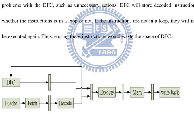
22
When a hit in DFC, the DFC eliminates one fetch from the I-cache and the subsequent decode,
which results in power saving. DFC results in 50% more power savings than an instruction
filter cache [4] and the average reduction in processor power is 34% [5]. Processor pipeline
with decode filter cache is shown in Fig 2-15. In Fig 2-15, there are five stages. When an
instruction is decoded, it will be stored into DFC. Once the instruction is executed again, it
can be accessed from DFC and will avoid I-cache to be accessed. DFC not only can decrease
the times of accessing I-cache but some actions of decoded stage. But there are some
problems with the DFC, such as unnecessary actions. DFC will store decoded instructions
whether the instructions is in a loop or not. If the instructions are not in a loop, they will not
be executed again. Thus, storing these instructions would waste the space of DFC.
DFC
I-cache
Fetch
Decode
Execute
Mem
write back
Chapter 3 The Design of Predecode Loop Buffer
In this chapter, we will present the asynchronous 2-way VLIW processor in the
beginning. Including pipeline architecture and basic components and branch instruction, we
show details in the chapter 3.1. Then we introduce the design of predecode loop buffer for the
target asynchronous two-way VLIW processor. Predecode loop buffer uses an easy and novel
method to decide whether loop would be replaced or stored, and we will decrease overheads
as far as possible. A miss of predecode loop buffer deals hardly with pipeline, but
Asynchronous Muller Pipeline only has 50% utilization that could help to solve some
problems. We will present our miss recovery mechanism in chapter 3.2.5.
3.1 Asynchronous 2-Way VLIW Processor
We use the 4-phase dual-rail data encoding method to implement asynchronous two-way
VLIW processor. It has its own instruction set architecture (ISA) and has six stages in pipeline.
In addition to R-type, I-type instruction that like MIPS, it also supports SIMD and MAC
instructions. We use the feature of Muller Pipeline to handle branch instruction.
3.1.1 Pipeline Architecture
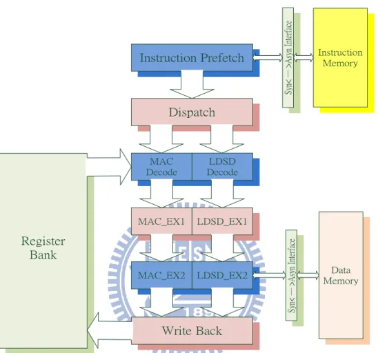
As mention previously, we use 4-phase handshake protocol and dual-rail data encoding method to control pipeline. The pipeline architecture of asynchronous two-way
24
Instruction Prefetch (IPF), Instruction Dispatch (IDP), Instruction Decode (ID), Execution 1 (EX1), Execution 2 (EX2) and Write Back (WB).
MAC Decode LDSD Decode Instruction Prefetch Write Back MAC_EX2 MAC_EX1 Dispatch Register Bank LDSD_EX1 LDSD_EX2 Data Memory Sy n< ─ > A sy n In te rf ac e Sy n< ─ > A sy n In te rf ac e Instruction Memory
Fig 3-1 The Pipeline Architecture of Asynchronous Two Way Processor
The followings are actions of the six stages of the target asynchronous two-way
VLIW processor:
1. Instruction Prefetch: According to PC (Program Counter), instruction would be
fetched from instruction memory via an sync/async interface. The interface can
transfer the encoding method of synchronous circuit and asynchronous circuit to
2. Instruction Dispatch: This stage would dispatch these instructions to appropriate
decode unit. Because our instruction is compressed, the last bit of the instruction
can be needed to decide if it can be executed in parallel with next instruction.
3. Instruction Decode: The major work of this stage is to decide instruction and
fetching operand. The instruction will be needed to generate the control signals
controlling its execution in following stages.
4. Execution 1 and Execution 2: We separate the execution stage into two stages,
Execution 1 and Execution 2. The Mac instruction is only executed in the left part
of EX2 stage. The Load and Store instruction are only executed in the right part of
EX2 stage. In addition to Mac, Load and Store instruction, other instructions can be
executed in both the left part and the right part.
5. Write Back: In this stage, the result can be written back to the correct destination
register. If the instruction does not need to write result back, this stage will be
bypassed.
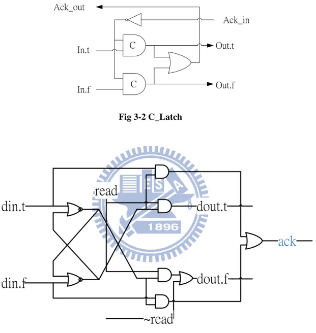
There are pipeline latches between each two stages. Because of asynchronous
pipeline latch is clockless, we use C-element to implement the pipeline latch that is
composed of C_latch. C_latch is shown in Fig 3-2. Another special component is the
asynchronous register. Each 1-bit register is made of four AND gates, two OR gates, and
26
register. The 1-bit register is shown in Fig 3-3.
Ack_in Ack_out In.t In.f Out.t Out.f C C Fig 3-2 C_Latch
din.t
din.f
dout.t
dout.f
read
~read
ack
Fig 3-3 The 1-bit Register
3.1.2 Branch Instruction
In this section, we present our efficient method to handle branch instruction. The
architecture is show in Fig 3-4. In Fig 3-4, I&V register is a component to control where
instruction are written into Buffer. Buffer stores the instructions that are already fetched.
The value of Dir register lets Prefetch unit know which part of instructions should be
fetched. The grey part of register is stand for timing of writing register.
Fig 3-4 Branch Handling Architecture
When branch instruction is taken, the MAC EX1 would send a stall control signal to
Stall unit and send target address to PC register and Dir register. Stall control signal lets
Stall unit send a bubble to next stage and clear the content of I&V register. Finally, PC Dispatch Prefetch MAC decode MAC EX1 LDST decode LDST EX1
…
pc pc+1 PC Buffer I & V |Dir | V | I | PC | PC’ PC stall ctl target address pc_mux Dir Dir Calculate PC’ Stall28
element. The Merge element is called pc_mux in Fig 3-5. However, there is a critical
issue that must be guaranteed, the timing issue. Because of branch instruction, PC
register is possibly written by different stages in our pipeline architecture. In our branch
handling architecture, there are three combinations when a branch instruction taken. The
combination of Valid token and Empty token are shown in Fig 3-5.
Empty
Valid
Empty
Valid
Valid
Empty
Empty
Valid
Empty
Empty
Empty
Valid
Instruction Prefetch Instruction Dispatch Instruction Decode Ex1 (a) (b) (c)Fig 3-5 The Combination of Valid Token and Empty Token
In Fig 3-5 (a) and (c), branch instruction would not produce any problem in our
branch handling architecture. In Fig 3-5 (b), because the next instruction of branch
instruction is too slow, so that it is still in Instruction Prefetch stage. At the same time,
branch instruction in EX1 stage is already completed and the result is generated. Thus,
would be written into PC register when it enters the Instruction Dispatch stage.
To solving this trouble, we assume some constraints for branch instruction. We
assume a time stamp, Td. The time stamp is that the next instruction of branch instruction
is completed in Dispatch stage and new pc address is sent from Dispatch stage. The time
stamp of branch instruction sending new target address from exe1 stage is Tb. It must be
guaranteed that Tb > Td. In other words, we must guarantee the case (b) and case (c) in
Fig 3-5 would not be happened.
3.2 Predecode Loop Buffer
This section will present the architecture of predecode loop buffer. As above-mentioned
in chapter 2, traditional loop detection would make some possible problem. In addition to
loop that must not be nested loop, the major trouble is that the frequently executed
instructions in loop buffer may be replaced by infrequently executed instructions. If the
infrequently executed instructions only execute sometimes, this replacement will become an
unnecessary action. For example, Loop 2 and Loop 3 are inside Loop 1. When the Loop 1
executes one time, the Loop 2 only executes two or three time and the Loop 3 executes
hundreds of times. In other words, Loop 2 only obtains few benefits from loop buffer.
Comparing with Loop 2, Loop 3 would get many advantages of loop buffer, because Loop 3
30
again. This replacement is an unnecessary operation. If Loop 1 also executes many times, the
unnecessary operation will become numerous. The example of program is shown in Fig 3-6.
Non-Branch Instruction Non-Branch Instruction Loop2 Loop3 Branch Instruction Branch Instruction Branch Instruction Loop1
Fig 3-6 The Example of Program
Although we take advantage of loop buffer, but there still exist repeated actions in
Instruction Decode stage. In Instruction Decode stage, it has to decode instruction and fetch
operands from register file. Fetching operand operations cannot be ignored, because the
operands of the same instruction would be different in every time of execution. Comparing
with fetching operands action of decoding instruction is always the same as previous
execution despite the instruction executing hundreds of times. Thus, Control signals are stored
keep the control signals to reduce some operations of Instruction Decode stage. Because the
control signals of instruction are more than the opcode of instruction, Predecode Loop Buffer
is bigger than traditional loop buffer. That is a tradeoff between area and performance. The
tradeoff is worth implementing, because the operations of Instruction Decode stage are one of
the major factors of performance of system. The details of Predecode Loop Buffer will be
presented at the following sections in this chapter. The Block Diagram of Instruction Decode
stage is shown in Fig 3-7.
MAC Decode LDST Decode Register Bank opcode opcode
Instruction of MAC Decode Instruction of LDST Decode
Control signal of MAC Ex1 Control signal of MAC Ex1 Register control signal Register control signal operands of MAC Ex1 operands of LDST Ex1 rd,rs,rt rd,rs,rt
32 F-reg Mode Controller
Instruction
Prefetch
Execute 1
Instruction
Decode
Instruction
Dispatch
Pipeline Latch Pipeline Latch Pipeline Latch F F Branch Information Table Branch ? Mode bit Information Predecode Loop Buffer PC Control Signal S Stall Miss Read Decoded signal Index Change Taken? Dir Dir Dir’ Dir S-reg F 0 S F PCFig 3-8 The Architecture of Predecode Loop Buffer
3.2.1 Overview
The architecture of Predecode Loop Buffer includes a Branch Information Table, a
Mode Controller, a Loop Buffer and three registers that include two mode registers and
an index register. The architecture of Predecode Loop Buffer is shown in Fig 3-8. Branch
Information Table would store some information of branch instruction, such as the taken
times of a branch, and information about this branch whether it would become hot or not.
The hot branch stands for that the branch is frequently executed. Mode Controller would
write information to Branch Information Table and mode registers. Every instruction
would be decided if it is accessed from Predecode Loop Buffer or stored the control
signals into Predecode Loop Buffer. Two mode registers are Store register (S-reg) and
Fast Access register (F-reg). When the value of S-reg is one, the control signals of
instruction have to be stored into Predecode after the instruction is completely decoded.
When the content of F-reg is one, the instruction can be accessed from Predecode Loop
Buffer and Instruction Prefetch unit can be bypassed. Thus, we need some elements to
bypass the Instruction Prefetch unit. These elements are DeMux and Merge. The DeMux
and Merge are shown in Fig 3-9.
Function block Function block In Sel.t Sel.f C C DeMUX Merge Out
Fig 3-9 The DeMux and Merge
When Sel.t equals to one and Sel.f equals to zero, the In signal will be passed to
34
only use a OR gate, because there are only one function block can receive the valid token
from DeMux and only on function block can pass valid token to Merge. Thus, another
function block would not work and it would be bypassed.
3.2.2 Branch Information Table
Branch Information Table (BIT) has four fields that including Tag, Execute Counter,
Frequent Flag and Pre-Frequent Flag. When a branch instruction is in the Instruction
Decode stage, Instruction Decode unit will send control signals to BIT. The BIT will be
searched by the PC value of the branch instruction and the control signals. If the
information of the branch instruction exists in BIT, the information of the branch
instruction would be accessed and be transferred to Mode Controller in EX1 stage.
Otherwise, the valid zero would be sent to Mode Controller. The Branch Information
Table is shown in Fig 3-10.
The PC of branch
Tag Execute
Counter FrequentFlag Pre-Frequent Flag
... ... ... ...
The reading action of BIT is in Instruction Decode stage and the writing action of
BIT is in EX1 stage. Although these actions are in different stages, they are possible to
produce a problem. When the Instruction Decode stage is completed, the valid token
should be in Ex 1 stage and Instruction Decode stage should be returned to zero. It stands
for the empty token. However, if the delay time of Ex 1 stage from this stage starts to
finish shorter than the delay time of returning Instruction Decode stage to zero, BIT will
be accessed and written at the same time. To avoid this trouble, we must provide that
writing BIT is after Instruction Decode stage returns to zero.
d1.t d1.f d2.t d2.f out1.t out1.f out2.t out2.f
Fig 3-11 The Mutual Exclusion
To achieving this goal, both read and write signals are connected to a Mutual
36
the faster input that arrives in ME and d2 is the slower input that arrives in ME. The out1
would become valid because d1 is faster. Although the d2 is also valid, out2 still is empty.
Out1 will become empty after d1 is returned to zero. Then d2 just can let out2 become
valid. This section finally presents the BIT block diagram and shows how BIT can be
bypassed. BIT block diagram is shown in Fig 3-12. If PC is sent to BIT, the data of
accessing BIT will become R_Information. Otherwise, the R_Information will be
inserted with valid zero. For writing of BIT, it is like the reading of BIT. When BIT must
be written new data, wack is inserted with one by BIT. On the other hand, wack will be
inserted with one as fast as possible.
Branch
Information
Table
PC Branch? D eM ux Merge R_Information D eM ux Merge wack W_Information write3.2.3 Mode Controller
The value of mode registers is decided by Mode Controller. Depending on the value
in mode registers, the instructions are decided if they are written into Predecode Loop
Buffer or are accessed from Predecode Loop Buffer. Thus, Mode Controller is an
important component in the architecture of Predecode Loop Buffer. There are three
modes in our Predecode Loop Buffer, including Direct Mode (DM), Fast Access Mode
(FAM) and Storage Mode (SM). DM means that the instruction will be fetched from
Instruction Memory. FAM means that the instruction will be fetched from Predecode
Loop Buffer. SM means that the control signals of the instruction must be written into
Predecode Loop Buffer after the instruction is completely decoded. In addition to the
mode registers, Mode Controller needs an extra register to calculate the count of hot
branch and the count of non-hot branch. The register is called “replace register”.
Depending to the value in this register, Mode Controller can decide the instruction of
Predecode Loop Buffer if it is frequently executed in recently period of execution.
Storage Fast
Access Direct
38
Fetch Mode Events
Direct Mode
(1) Predecode Loop Buffer misses
(2) (BIT hit)&&(Frequent Flag and Pre-Frequent Flag are 0s)&&(Execute
Counter < threshold)
(3)(BIT hit)&&(Frequent Flag or Pre-Frequent Flag are 1s)&&(branch is not
taken) Fast Access
Mode
(BIT hit)&&(Frequent Flag or Pre-Frequent Flag are 1s)&&(branch is taken)
Storage
Mode
(BIT hit)&&(Frequent Flag and Pre-Frequent Flag are 0s) &&(branch is
taken)&&(Execute Counter ≧ threshold)
Table 3-1 The Transition Events of Mode
The possible transitions of Mode are shown in Fig 3-13. The events that cause mode
transitions are shown in Table 3-1. When the BIT is accessed by a branch instruction, the
replace register is also accessed. If the hot branch is taken, Mode Controller would let the
replace register be decreased by one. Otherwise, if the non-hot branch is taken, Mode
Controller would let replace register be increased by one. If the value overflows after
increasing by one, the data is Predecode Loop Buffer are not frequently executed in
recent period of execution. Thus, Mode Controller would clean the Frequent Flag of
Branch Information Table and Pre-Frequent Flag would not be cleaned. Although
Depending upon the value of Pre-Frequent Flag, the fetch mode will be changed to FAM.
A program usually is composed of many phases. When the program enters the program
phase, it will execute instructions in the same block. That block usually contains some or
many of loops. In other words, when the program enters another program phase,
Frequent Flag should be flush because branch information in BIT may be useless. The
Transition Phase and Program Phase are shown in Fig 3-14.
Mode Controller lets BIT be always in two kinds of phase. One is writing phase and
another is monitor phase. In writing phase, the Frequent Flag is cleaned. At this time,
BIT enters another program phase. In monitor phase, it means that at least one Frequent
Flag of BIT is one. At this time, BIT will stay at the same program phase.
Writing Monitoring
Transition Phase Program
Program Phase 1 Program Phase 2 Program Phase 3
Program Phase N
... ...
Fig 3-14 The Transition Phase and Program Phase
40
the two figures.
DeMux Information Branch Mode Controller Taken Merge w_information w_ack controller_complete
Fig 3-15 The Block Diagram of Mode Controller
3.2.4 Procedure of Predecode Loop Buffer
As above sections, every component of Predecode Loop Buffer is presented. In this
section, we will introduce the procedure of Predecode Loop Buffer. The procedure
includes four steps:
Step 1: Because the Execution Count of branch instruction smaller than threshold, Mode
Controller will not change the value in mode register.
Step 2: When the Execution Count of branch instruction equals to the threshold, Mode
Controller will set S-reg and Frequent Flag to one. The control signals of next
Step 3: The Frequent Flag of branch instruction is one, so the next instruction is existed
in Predecode Loop Buffer. Thus, Mode Controller sets the F-reg to one, and the
next instruction can be accessed from Predecode Loop Buffer.
Step 4: When a miss is produced, it stands for the next instruction that must be fetched
from Instruction Memory. In next section, we will present details about miss
recovery mechanism of Predecode Loop Buffer.
ADD R3,R2,R1 ADD R6,R4,R5
BEQ R9,R3,target NOP
... ... SUB R3,R2,R1 SUB R6,R4,R5 Instruction Prefetch Instruction Decode EX1 Instruction Dispatch BEQ SUB ADD
Fig 3-16 A Frequent Loop in a Program
Fig 3-16 shows a frequent loop in a program. When the BEQ instruction is decoded
first time, the information of BEQ cannot be accessed from BIT. Because this is the first
time to execute, the information of the BEQ are all zero. As soon as the decode stage is
42
mechanism is implemented in our processor, much design overhead can be reduced,
Mode Controller only needs to wait the result of BEQ whether it is taken or not. If the
BEQ is taken, Mode Controller will add Execution Counter by one and decide which
mode should be written into mode registers. Otherwise, Mode Controller will pass the
action of increasing Execution Counter. We assume the BEQ is taken. Because the BEQ
is executed first time, the mode will not be changed. At the same time, the SUB
instruction will be flushed by branch handling mechanism. Every time the BEQ comes
before Execution Counter equals to the threshold, these actions will be repeated. When
the value of Execution Counter equals to the threshold, Mode Controller sets S-reg to
one in EX1 stage. Thus, the control signals of next instruction should be written into
Predecode Loop Buffer. In addition to the control signals of ADD instruction, some of
the control signals in Instruction Prefetch and Instruction Dispatch also need to be stored.
At this moment, storing these signals may have a problem. An instruction in our VLIW
processor may be dispatched two times, because the instructions are stored in
Instruction 1 Instruction 2 VLIW Instruction
Instruction 1 NOP Instruction 1 Instruction 2
NOP Instruction 2
Dispatch
(a)
(b)
Fig 3-17 The Cases of the Instruction
Instruction 1 Instruction 2 Index Pipeline Latch p-bit p-bit change Dir Taken
Fig 3-18 The Hardware Solves the Instruction with Same Address
If the instruction 1 and instruction 2 can be executed in parallel, the last bit of
instruction 1 is one. If the last bit of instruction 1 is zero, the two instructions cannot be
44
would not produce any trouble because the two instructions can be executed in parallel.
In Fig 3-17 (a), storing control signal would produce a problem because the two
instructions cannot be executed in parallel. That is because they have same PC values.
The instruction must be dispatched two times. Thus, when this instruction is fetched
from Predecode Loop Buffer, we cannot decide which one is need.
To solve this problem, we add an XOR gate, an OR gate and an Index register. Fig
3-18 shows that the hardware solve that the instruction with same address. At first, we
can decide if the instruction is a complete VLIW instruction or half through Dispatch
stage according to p-bit. The p-bit of two instructions are connected to an OR gate. The
output of OR gate is called change bit. Index register stores the value of direction of the
VLIW instruction in EX1 stage. Then change bit and the output of Index register are
connected to a XOR gate. Finally, the index of next VLIW instructions through Dispatch
stage is the output of XOR gate.
The output would be computed in Decode stage and written into Index register in
EX1 stage. If the value of Index register is 1, the direction of instruction is left.
Otherwise, the direction of instruction is right. Table 3-2 shows the relationship between
p-bit of Instruction 1 p-bit of Instruction2 Change
0 0 0
0 1 1
1 0 1
1 1 Not Used
Table 3-2 The Relationship between P-Bit and Change Bit
Change Index of this instruction Index of next instruction
0 0 1
0 1 0
1 0 0
1 1 1
Table 3-3 The Relationship between Change Bit and Index
After we solve the trouble of writing data to Predecode Loop Buffer, every
instruction can be written and accessed at correct place. The next times of the BEQ that
is executed, Mode Controller receives the data from BIT. Because the Frequent Flag is
one, Mode Controller will set the F-reg to one in EX1 stage. The F-reg has the timing
46
possibly written by different stages. When the ADD instruction is executed again after
F-reg is set to one, the current instruction can be fetched from Predecode Loop Buffer in
Instruction Dispatch stage. The Instruction Prefetch and Dispatch stages can also be
bypassed. The bypass mechanism can also be implemented with DeMux and Merge pair.
When S-reg is set to 1, Predecode Loop Buffer does not have information that we
need. Otherwise, if F-reg is set to one, Predecode Loop Buffer already has data that we
need. Finally, there are three cases that would change the value of F-reg to zero. First, a
miss of Predecode Loop Buffer causes the information of instruction of loop that we
need is lost. Second, the branch instruction is hot branch, and it is untaken at this time.
Third, there are other branch instructions to change Mode.
3.2.5 Miss Recovery Mechanism
The major work of miss recovery mechanism is recovering the action of every stage
and fetching the miss instruction again from Instruction memory. To achieve this work,
we must flush that the wrong information in every stage. Fortunately, 4-phase dual-rail
pipeline only have 50% utilization and Predecode Loop Buffer is read in Instruction
Dispatch. In other words, we just need to deal with the miss in Instruction Dispatch,
because Instruction Prefetch and Instruction Decode stages are empty.
occurs, some signals and the value in F-reg should be re-transferred. At first, the value in
F-reg is changed to zero. The action can provide that the next instruction is with the
correct mode. Then the PC address of the miss instruction will be written into the PC
register. The action can provide that the miss instruction is fetched from instruction
memory with correct address.
Finally, we must flush this miss instruction. We take an easy and quick method to
solve this issue. In Fig 3-4, there is a stall unit. Thus, the miss signal will be sent to the
stall unit. Then the stall unit will insert a NOP to the next stage. This action is almost like
the branch instruction is taken and a bubble must be inserted to the next stage. Although
Predecode Loop Buffer can correctly work, there are some places that can be improved.
We will present these future works in chapter 5.
Fig 3-19 Miss Recovery Mechanism
Instruction
Dispatch
Pipeline Latch Predecode Loop Buffer Stall Miss Decoded signal F.A D.A PC48
Chapter 4 SIMULATION RESULT
In this chapter, we will show the area and timing simulation of Predecode Loop
Buffer. The design was synthesized by Design Compiler under TSMC 0.13μ m2process.
First, we present the area of every element including C-element, 1-bit register, Branch
Information Table, Predecode Loop Buffer. We show the timing simulation of the design.
Fig 4-1 shows the timing diagram of Predecode Loop Buffer.
Fig 4-1 The Timing Diagram of Predecode Loop Buffer
4.1 Area Simulation
4-2 presents the area of Predecode Loop Buffer, Branch Information and Mode
Controller comparing with asynchronous two way processor.
1-bit register C_Latch C-element
Cell Area (μ m2) ~54 ~41 ~21
Table 4-1 the area of basic element in our Predecode Loop Buffer
BIT Predecode Loop Buffer Mode Controller Processor
Cell Area (μ m2) ~8600 ~240000 ~1200 ~900000
Ratio 0.95% 26.67% 0.1% 100%
Table 4-2 the area compares with asynchronous two way VLIW processor
The cell area of Predecode Loop Buffer is big, because it stores the control signals.
The control signals are bigger than instructions, so the Predecode Loop Buffer is bigger
than traditional loop buffer. The BIT and Mode Controller are small components in our
design.
4.2 Timing Simulation
50
BIT Predecode Loop Buffer Mode Controller
Delay (ns) 4.39 7.41 4.76
Chapter 5 CONCLUSIONS AND FUTURE WORKS
In this thesis, we propose a novel loop detection. It is implemented on an asynchronous
two way VLIW processor. Because the decoded instruction is a major operation of system, the
control signals are stored after the instruction is decoded to reduce some actions of instruction
decode. We use the bigger loop buffer to replace traditional loop buffer, this is a tradeoff.
Predecode Loop Buffer not only can decrease the accessed times of Instruction memory but
can decrease the operations of Instruction Dispatch and Instruction Decode stages.
Because the instructions are stored in compressed form, the instructions may be divided
to two parts and transferred to EX1 stage. When the control signals of the instructions are
stored in Predecode Loop Buffer, it will produce a problem. To solve this problem, we add
some components to differentiate the instruction that may be divided. The design was
synthesized by Design Compiler under TSMC 0.13μ m2process. The area of Predecode Loop
Buffer is 240000μ m2 and its delay time is 7.41 ns.
Although Predecode Loop Buffer can decrease the instruction memory access times, it is
bigger than traditional loop buffer. In addition to the control signals is stored in Predecode, the
instruction is compressed that also make less instruction to be stored in Predecode Loop
Buffer. It is an issue that the control signals of the instruction how can be efficiently stored in
52
REFERENCES
[1] Lea Hwang Lee, Bill Moyer, John Arends, “Instruction Fetch Energy, Reduction Using Loop Caches For Embedded Applications with Small Tight Loops”, in Proc. Int. Symp.
Low Power Element. Design, 1999, pp. 267-269.
[2] ChiTa Wu, Ang-Chih Hsieh, and TingTing Hwang, “Instruction Buffering for Nested
Loops in Low-Power Design”, in Circuits and Systems, 2002. ISCAS 2002. IEEE
International Symposium. vol. 4, 2002, pp. 81-84
[3] Na Ra Yang, Gilsang Yoon, Jeonghwan Lee, Jong Myon Kim, Intae Hwang, Cheol Hong Kim, “Loop Detection for Energy-aware High Performance Embedded Processors”, in
Asia-Pacific Services Computing Conference, 2008, pp. 1578-1583
[4] Weiyu Tang, Rajesh Gupta, Alexandru Nicolau, “Design of a predictive Filter Cache for Energy Savings in High Performance Processor Architectures”, in Int’l Conf. on Computer
Design, 2001
[5] Weiyu Tang, Rajesh Gupta, Alexandru Nicolau, “Power Savings in Embedded Processors through Decode Filter Cache”, in Design, Automation and Test in Europe Conference and
Exhibition, 2002, pp. 443-448
[6] Weiyu Tang, Arun Kejariwal, Alexander V. Veidennbaum and Alexandru Nicolau, “A Predictive Decode Filter Cache for Reducing Power Consumption in Embedded Processors”, in Transactions on Design Automation of Electronic Systems. vol 12, 2007
[7] T. Anderson and S. Agarwala, “Effective Hardware-Based Two-way Loop Cache for High Performance Low Power Processors”, in Proc. Int. Conf. Comput. Design, 2000, pp. 403-407.
[8] Ya-Lan Tsao, Wei-Hao Chen, WenSheng Cheng, Maw-Ching Lin and ShyhJye Jou, “Hardware Nested Looping of Parameterized and Embedded DSP Core”, in SOC
Conference, 2003. Proceedings. IEEE International, 2003, pp. 49-52.
[9] Marcos R. de Alba, David R. Kaeli, “Runtime Predictability of Loops”, in Workload
Characterization, 2001. IEEE International Workshop, 2001, pp. 91-98.
[10] Timothy Sherwood and Brad Calder, “Loop Termination Prediction”, in ISHPC, 2000, pp.73-87.
[11] M. Monchieroa, G. Palermoa, M. Samia, C. Silvanoa, , V. Zaccariab, R. Zafalonb, “Low-power branch prediction techniques for VLIW architectures: a compiler-hints based approach”, in INTEGRATION, 2005, pp.515-524.