Semiconductor laser for all-optical switching between medium-wave
band and long-wave band in optical fiber communication
Chi-Chia Huang
a, Yi-Shin Su, and Ching-Fuh Lin
a, b aGraduate Inst. of Electron-Optical Engr., National Taiwan Univ., Taiwan
b
Dept. of Electrical Engr. and Graduate Inst. of Electronics Engr., National Taiwan Univ., Taiwan
ABSTRACT
Dual-wavelength semiconductor laser with wavelength separation as large as 203 nm is reported. With the short-wavelength mode located in 1345.4 nm and the long-short-wavelength mode in 1548.6 nm, the operation region of the laser system covers both the medium-wave band (1300 nm region) and long-wave band (1500 nm region) in optical communication. Random selection of oscillating wavelength position between 1345.4 nm and 1548.6 nm is also possible with fixed wavelength separation. This broadband laser system provides an opportunity for all-optical switching between the medium-wave band and long-wave band in optical communication.
Keywords: all-optical switching, dual-wavelength semiconductor laser, nonidentical multiple quantum wells, optical
fiber communication, reflected-type grating telescope configuration.
1. INTRODUCTION
With the booming of network, optical fiber communication grows up with a rapid speed due to its large transmission capacity, high speed, and low loss. Recently, the transmission bandwidth of optical fiber is larger than 300 nm, ranging from 1250 nm to 1600 nm with the removing of OH absorption around the 1400 nm band. Traditionally, the bandwidth of optical fiber can be divided into two sections for optical communication: the medium-wave band (1250 nm ~ 1350 nm) and the long-wave band (1450 nm ~ 1600 nm). Signals transmitted in the medium-wave band have lower dispersion, whereas those transmitted in long-wave band suffer from lower loss. For the cross connection between these two bands, a broadband optical switch is necessary.
Recently, there are several ways for constructing an optical switch. For example, two waveguides can be coupled with each other by the use of an electro-optic modulator, and the channel switching is controlled by the external electric signal [1]. This structure is the so-called waveguide-type Mach-Zehnder interformeter [2], and can be fabricated by fiber laser or semiconductor laser. In addition, four-wave mixing (FWM) can also be applied to construct an optical switch [2, 3]. Lately, very fast all-optical demultiplexing up to 500 Gb/s has been accomplished using FWM in a PANDA fiber [4]. On the other hand, FWM in SOAs is expected to be more suitable for demultiplexing because of its compact size and no wavelength limitation, as compared with FWM in fibers [5]. However, the conversion efficiency of FWM is not high due to the weak nonlinear effect, especially for fiber laser. In addition, the operation spectral range is limited by the gain bandwidth of the laser gain medium [5]. Another promising method for constructing an optical switch is using the gain-competition mechanism in a dual-wavelength laser system. This last method has the best conversion efficiency. However, the operation spectral range is also significantly limited by the laser gain bandwidth.
The optical switch constructed by semiconductor laser has the advantages of small size, easy integration, and high efficiency. However, the bandwidth of traditional semiconductor laser is not large enough to cover both the medium-wave band and long-medium-wave band simultaneously. Therefore, channel switching between these two bands usually has to be accomplished by another method which needs two lasers. That is, the optical signal is first received and transformed into electric signal, which is then switched to a new channel by electronic devices and transformed back into optical signal. The switching speed of this method is not high due to the delay caused by the optic-electric and electric-optic conversion. What’s worse, the system is more complicated due to the integration of multiple lasers, compared with those methods that require only single laser. In this work, we will report a dual-wavelength laser system with a record wavelength separation larger than 200 nm. The short-wavelength mode (SWM) and the long-wavelength mode (LWM) are located in 1345.4 nm and 1548.6 nm, respectively. Moreover, at a fixed mode spacing, we can randomly choose the
position of the two modes from 1345.4 nm to 1548.6 nm. This laser system is a promising device for all-optical switching between the medium-wave band and long-wave band in optical communication.
2. EXPERIMENT
2.1 Broadband gain medium
To obtain a wide dual-wavelength separation, we need a broadband superluminiscent laser diode (SLD) as the gain medium. Quantum-well (QW) engineering is a convenient and widely used approach to broaden the bandwidth of SLDs. This scheme includes using a single QW with simultaneous transitions of n = 1 and n = 2 states [6, 7], and using nonidentical QWs [8-11]. Because the simultaneous transitions of n = 1 and n = 2 energy states in identical QWs rely strongly on the device lengths [6, 7], nonidentical multiple quantum wells (MQWs) were recently been widely used for broadband purposes.
However, the nonuniform carrier distribution among the MQWs has to be taken care of when designing a broadband SLD with nonidentical MQW structure [12-15]. Nonuniform carrier distribution means that each QW of the MQW structure accumulates a different number of carriers, so their corresponding emission intensities are not equal. Thus, the overlap of the individual spectrum from each type of QW, weighed by its corresponding emission intensity, does not directly result in a broadband spectrum. Therefore, the design of nonidentical MQW structures for broadband purposes is not intuitively straightforward.
Our design procedure for the broadband SLD is described with detail in [16]. The designed QW structure of the SLD is shown in Fig. 1. A separate confinement heterostructure (SCH) is formed in connection with the wells. The SCH layer has a thickness of 120 nm. The wells are separated by 15-nm-wide In0.86Ga0.14As0.3P0.7 barriers. There are five
QWs in the SLD: two 8.7-nm In0.53Ga0.47As QWs and three 6.0-nm In0.67Ga0.33As0.72P0.28 QWs. The three 6.0-nm
In0.67Ga0.33As0.72P0.28 QWs are placed near the n-cladding layer, whereas the two 8.7-nm In0.53Ga0.47As QWs are placed
near the p-cladding layer. Table I shows the emission wavelengths corresponding to the energy levels of each QW calculated using the Luttinger-Kohn method [17].
In our experiment, we use laser diodes (LDs) with straight waveguide. This is because that, compared with the tilt or bent waveguide SLDs, the straight one has lower loss and lower threshold current. This can facilitate the tuning of the long-wavelength mode because the long-wavelength mode is very loss-sensitive. The length of the device was about 300 µm. No facet coatings were applied to the device. The measured emission spectrum of the LD is shown in Fig. 2. The Fabry-Perot resonance of the straight waveguide is located in 1370 nm with threshold current about 143 mA. To avoid the Fabry-Perot resonance, the operation current can not be too much larger than 143 mA for dual-wavelength tuning. This limits the operation bandwidth of the laser system.
Fig. 1. Designed QW structures: wide QW, In0.53Ga0.47As, 8.7 nm; narrow QW, In0.67Ga0.33As0.72P0.28, 6.0 nm, 6.0 nm; barrier, In0.86Ga0.14As0.3P0.7, 15 nm; SCH region, In0.86Ga0.14As0.3P0.7, 120nm.
TABLE I. Calculated Transition Wavelengths Corresponding to the Bounded Energy States of the Nonidentical MQWs of the Designed SLD
n 8.7-nm In0.53Ga0.47As Double QW (µm) 6.0-nm In0.67Ga0.33As0.72P0.28 Triple QW (µm) 1 2 3 1.54 1.46 1.18 1.3 1.24 Unbounded P N
Fig. 2. Measured emission spectrum of the SLD
2.2 External cavity and operation condition
In addition to a broadband gain medium, the laser cavity has also to be carefully engineered for large tuning range. Experiment shows that the loss in the external cavity has a significant influence on the oscillation of the wavelength above 1500 nm. Therefore, the design purpose of the external cavity is to minimize the cavity loss. However, due to the large size of the holding stages and optical components, the cavity with minimum loss is very difficult to obtain. In addition, due to the interaction between the two lasing modes, the optical path in the external cavity has to be modified under different spectral separation to minimize the loss.
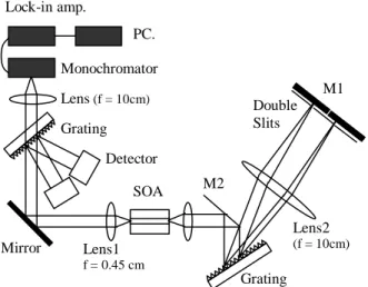
The external cavity we constructed is of reflected-type grating telescope configuration. For the purpose of easy tuning, the laser system is constructed as shown in Fig. 3. Two collimators with f = 4.5 mm and NA = 0.55 are used to collimate the light beams emitted from two facets of the SOA. The coupling efficiency of the collimators is about 70%. The grating is 600 lines/mm and is Au-coated. Its efficiency is about 80%. A lens with f = 10 cm is placed at 10 cm from both the grating and the mirror M1. The feedback mirror M1 is composed of two physically separated mirrors for the purpose of easy alignment [18, 19]. To be sure, the two mirrors that consist of M1 are parallel placed. This is in comparison with the new cavity configuration that will be discussed later. On the other hand, a thin mirror M2 is introduced to minimize the grating loss [18, 19]. In addition, the position of Lens2 has to be modified for better
Fig. 3. Experimental setup
1250 1300 1350 1400 1450 1500 1550 1600 0.0 0.5 1.0 1.5 2.0 2.5 3.0 04291 300µm straight em is si o n i n te n si ty ( a .u .) wavelength (nm) 149 mA 146 mA 143 mA 140 mA 136 mA 132 mA 128 mA SOA Lens2 (f = 10cm) Lens1 f = 0.45 cm Grating M1 Double Slits Detector M2 Mirror Grating Lens (f = 10cm) Monochromator PC. Lock-in amp.
alignment under different wavelength separation [19]. With the cavity configuration shown in Fig. 3, the maximum achievable dual-wavelength separation is about 191 nm, as demonstrated in [19].
In the laser system shown in Fig. 3, the work of wavelength tuning is performed by the moving of the double slits in front of mirror M1 [18]. This is a very convenient way for wavelength tuning. However, the cavity configuration shown in Fig. 3 is not the one that has the minimum loss. For the purpose of low loss and large wavelength separation, a new cavity configuration as shown in Fig. 4 (a) is used. In this configuration, Lens2 and the double slits are removed. Therefore, the grating diffracted light beam directly impinges on the feedback mirrors M3 and M4. Note that unlike the configuration shown in Fig. 3, now M3 and M4 are not parallel placed. In fact, the optimized direction of M3 and M4 are determined by the oscillating wavelength that we choose. The reason is as follows. The direction of the grating diffracted light beam is a function of wavelength. In addition, the facet of a feedback mirror has to be normal to the incident light beam to obtain maximum reflection efficiency. Therefore, when the oscillating wavelengths that we choose are changed, M3 and M4 have to be rotated so that their facets are normal to the incident direction of the new light beam. In fact, it is apparent that in the configuration shown in Fig. 4 (a), wavelength tuning is performed by the rotation of M3 and M4. In addition, since Lens2 is removed in the configuration shown in Fig. 4 (a), the alignment of the optical path is much easier than that using the configuration shown in Fig. 3. However, the drawback of this configuration is the inconvenience in the tuning of small wavelength separation because the mirrors M3 and M4 may block with each other.
However, although the introduction of M2 has significantly lowered the loss caused by the grating, it has also made the whole system complicated. A modification is done to the cavity configuration shown in Fig. 4 (a), and is shown in Fig. 4 (b). In Fig. 4(b), the mirror that is responsible for the feedback of the SWM (M3) is removed, and the SWM is reflected by the grating directly back to the SOA. On the other hand, the feedback of the LWM is still performed by the mirror M4. In addition, a 50/50 coupler is placed at the laser output. Because the coupler can reflect about half of the laser power back to the SOA, it can reduce the loss of the laser system and thus large spectral separation can be obtained. However, the direction of the coupler can not be directly normal to the light beam, and has to be carefully engineered. The reason is as follows. Since the coupler can reflect part of the laser power back to the SOA, there is an extra cavity formed between the facets of the coupler and SOA. Therefore, if the reflection efficiency
(a)
(b)
Fig. 4. Modified experimental setup. (a) Removing Lens2. (b) Removing mirror M2 and adding a coupler at the output end. M4 SOA Lens1 f = 0.45 cm Grating 50/50 coupler To OSA M3 SOA Lens1 f = 0.45 cm Grating To OSA M4 M2
of the coupler is too high, an undesired resonant mode will appear. Consequently, the direction of the coupler has to be slightly modified to avoid this undesired resonant mode.
The procedure for the optical component alignment in Fig. 4 (b) is as follows. First, the grating is placed and rotated such that the wavelength 1345.4 nm (this is the wavelength we chose as the SWM) is reflected back to the SOA by the grating. Then, the coupler and mirror M1 are placed for the tuning of the LWM.
2.3 Experimental results
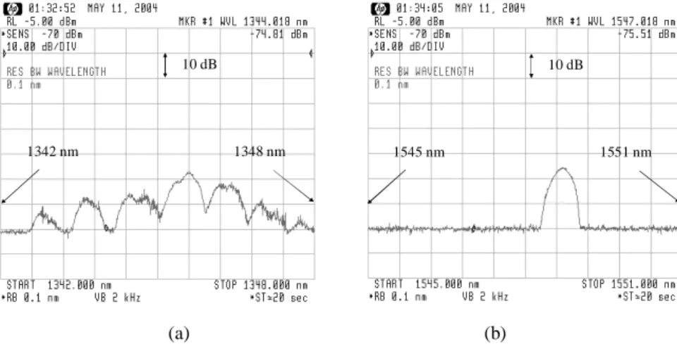
Fig. 5 shows the measured spectrum. With the SWM located in 1345.4 nm and the LWM located in 1548.6 nm, the wavelength separation is as large as 203 nm. The detailed spectra for the SWM and LWM are also shown in Figs. 6 (a) and (b), respectively. Several significant side modes appear in the spectrum shown in Fig. 6 (a). These side modes are the Fabry-Perot modes arising from the direct feedback of the SWM by the grating. This phenomenon can be eliminated if we use the cavity configuration shown in Fig. 4 (a) instead the low loss one shown in Fig. 4 (b) at the cost of smaller tuning range.
Disregard of the side modes shown in Fig. 6 (a) that is caused by the cavity configuration, the side mode
Fig. 5. Measured spectrum with 203 nm wavelength separation.
(a) (b)
Fig. 6. Detailed spectra of each mode. (a) Spectra of 1345.4 nm. (b) Spectra of 1548.6 nm. Separation > 203 nm 10 dB 1345.4 nm 1548.6 nm 1342 nm 1348 nm 10 dB 1545 nm 1551 nm 10 dB
suppression ratio (SMSR) of the laser system is about 23 dB. Although the 23 dB SMSR has been larger than the previous work demonstrated in [19], it is expected that the actual SMSR of the laser system should be better than the measured one. The reason is as follows. Note that the background noise in the spectrum of Fig. 5 is very flat, indicating that this noise is not the amplified spontaneous emission (ASE) noise that comes from the laser system. Instead, this noise is introduced by the measurement system, as is the case mentioned in [18, 19]. However, the measurement system we used in Fig. 4 is an optical spectrum analyzer (OSA), which is different from the one used in [18, 19]. Consequently, the mechanisms that cause the measurement noise are not the same. In Fig. 4, the measurement noise mainly comes from the low coupling efficiency of the laser output light to the optical fiber connected to the OSA. The reason is as follows. The best coupling efficiency is obtained when the output light beam is incident normally on the facet of the fiber. However, the fiber facet then appears as a feedback mirror and returns light back to the external cavity, influencing the oscillation of the lasing modes. Therefore, the direction of the fiber facet has to be slightly “misaligned” to avoid the undesirable effect. Therefore, the coupling efficiency of the output light to the OSA fiber is only about 40%, and the measured SNR is influenced significantly by the measurement noise.
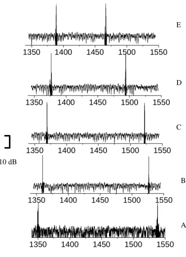
Fig. 7 shows the measured spectra under wavelength separation 191, 168.1, 154.9, 118.2 and 77.8 nm. The smallest wavelength separation that can be tuned is less than 10 nm Moreover, at fixed wavelength separation, we can randomly choose the position of the two modes from 1345.4 nm to 1548.6 nm as long as the balance between the gain
Fig. 7. Measured spectra of different wavelength separation. A: 191 nm (1350.3 nm ~ 1541.3 nm); B: 168.1 nm (1361.0 nm ~ 1529.1 nm); C: 154.9 nm (1369.8 nm ~ 1524.7 nm); D: 118.2 nm (1377.4 nm ~ 1495.6 nm); E: 77.8 nm (1390.4 nm ~ 1468.2 nm). 1350 1400 1450 1500 1550 1350 1400 1450 1500 1550 1350 1400 1450 1500 1550 1350 1400 1450 1500 1550 1350 1400 1450 1500 1550 10 dB Wavelength (nm) A B C D E
and the loss is properly adjusted. That is, there is no ‘gap’ where dual-wavelength operation is forbidden. Although the wavelength tuning is somewhat difficult to be achieved with the setups shown in Figs. 4, it is an easy task when using the configuration shown in Fig. 3 as demonstrated in [18, 19].
3. Discussion
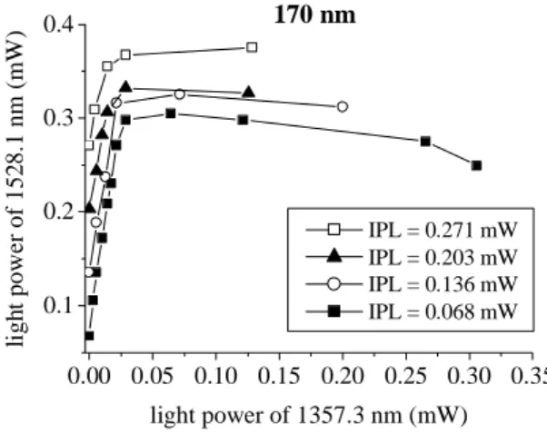
The possibility of large mode spacing is due to the following reasons. First, as discussed above, the gain spectrum of the nonidentical MQWs is broad. Second, at large mode spacing, the two wavelengths are nearly contributed from two different QWs. Therefore, competition at large mode spacing is weak because the carrier transportation betweenQWs is a relatively slow process, compared to the intraband relaxation in the same well. In reality, at mode spacing larger that 170 nm, competition plays a more important role than competition in the laser system [19, 20]. Under anti-competition, the SWM can provide the LWM with some optical gain, as shown in Fig. 7 for wavelength separation 170 nm. As mentioned previously in section 2.2, wavelengths above 1500 nm are very loss sensitive. Since anti-competition can provide the LWM with some extra gain, the loss encountered by the LWM can thus be balanced. Therefore, this phenomenon also contributes to our achieving a broadband tuning range.
Under our operation current (146 mA), wavelength below 1343 nm is difficult to oscillate. Increasing the injection current can facilitate the tuning of the SWM due to the large gain at the short-wavelength side under high injection current level [21]. However, since the gain medium we used is a Fabry-Perot laser diode (FPLD), increasing the injection current also runs the risk of having the Fabry-Perot start oscillating. In addition, the LWM is difficult to oscillate under high injection current. This is because that increasing the injection current will cause an increase in temperature, which may lead to the increase of the gain for the SWM and the decrease of the gain for the LWM [21]. The reason is due to the strongly temperature-dependent Fermi-Dirac distribution, which favors carriers in high-energy states at large temperature [21]. Therefore, increasing the injection current can decrease the tuning range at the long-wavelength side due to this temperature effect. However, under higher injection current, the SWM can provide the LWM with more optical power through mode anti-competition [19, 20]. Therefore, the overall impact that the current increase will have on the LWM tuning range still need more study after we applied an anti-reflection coating to our FPLD to suppress the Fabry-Perot resonance for high current operation.
As mentioned above in section 1, the applications of all-optical switch using semiconductor lasers are limited by the laser gain bandwidth. In fact, due to the narrow bandwidth of the semiconductor laser, many of today's optical switches must first convert optical signals into electrical signals, read them, process them and then convert them back to optical signals before sending them on their way. This conversion causes bottlenecks that slow down the routing process. Since we have built a tunable dual-wavelength laser system with maximum achievable wavelength separation larger than 200 nm, channel switching within this spectral range can be accomplished with single semiconductor laser. Therefore, the process of electric-optic and optic-electric conversion is unnecessary, and the switching speed can be
Fig. 7. Relation between the powers of the SWM and LWM at wavelength separation 170 nm 0.00 0.05 0.10 0.15 0.20 0.25 0.30 0.35 0.1 0.2 0.3 0.4 170 nm li gh t pow er of 152 8. 1 nm ( m W ) light power of 1357.3 nm (mW) IPL = 0.271 mW IPL = 0.203 mW IPL = 0.136 mW IPL = 0.068 mW
improved. In fact, simultaneous generation of eight channels with channel spacing 20 nm has been achieved using single semiconductor laser [22]. The configuration of the multi-channel laser system is similar to that shown in Fig. 3 except that the external cavity is modified for multi-channel purpose. This achievement further proves that our laser system has the potential for all-optical channel switching in wavelength division multiplexing.
Our broadband dual-wavelength laser system also provides a new mechanism for wavelength conversion. In the past, wavelength conversion using the mechanism of mode competition will make the signal inverted. This is because that mode competition is of negative power correlation. Therefore, a high bit in the original channel will be transformed into a low bit in the converted channel. However, in our broadband laser system, both of the SWM and LWM can have their power increased simultaneously within a certain power range due to anti-competition (refer to Fig. 7), which is opposite to the traditional mode competition [23, 24].This positive power correlation provides us with an opportunity for non-inverted wavelength conversion.
4. Conclusion
With the booming of network, optical fiber communication grows up with a rapid speed due to its large transmission capacity, high speed, and low loss. For large transmission capacity, multi-channel transmission is the trend in optical fiber communication. However, many of nowaday optical switches have to involve electric-optic and optic-electric conversion when performing channel switching. These conversions cause bottlenecks that slow down the routing process. On the other hand, recent all-optical switches suffer from small operation spectral range due to the narrow gain bandwidth of the laser device. In this work, we have reported a broadband dual-wavelength laser system with a record wavelength separation as large as 203 nm. In addition, wavelength tuning is possible within this spectral range. The cavity configuration has to be carefully designed to minimize the system loss. However, tradeoff exists between low loss and tuning convenience. With the SWM located in 1345.4 nm and the LWM in 1548.6 nm, this laser system acts as a promising device for all-optical switching between the medium-wave band and long-wave band in optical communication. In addition, the phenomenon of mode-anti-competition provides us with an opportunity for non-inverted wavelength conversion. Further broadening of the tuning range is possible if we applied an anti-reflection coating to the FPLD to suppress the Fabry-Perot resonance for high current operation.
REFERENCES
[1] Robert G. Hunsperger, Integrated Optics: Theory and Technology, Springer-Verlag, 127-164 (1992).
[2] Ching-Fuh Lin, Optical components for communications: Principles and Applications, Kluwer Academic Publisher (2004).
[3] Robert W. Boyd, Nonlinear Optics, Academic Press Inc. (1992).
[4] T. Morioka, H. Takara, S. Kawanishi, T. Kitoh, and M. Saruwatari, Electron. Lett. 32, 833 (1996). [5] M. Saruwatari, IEEE Journal on Selected Topics in Quantum Electron. 6, 1363 (2000).
[6] A. T. Semenov, V. R. Shidlovski, and S. A. Safin, Electron. Lett. 29, 854 (1993). [7] T.R. Chen, L. Eng, Y. H. Zhuang, and A. Yariv, Appl. Phys. Lett. 56, 1345 (1990). [8] C.-F. Lin, B.-L. Lee, and P.-C. Lin, IEEE Photon. Technol. Lett. 8, 1456 (1996).
[9] X. Zhu, D. Cassidy, M. Hamp, D. Thompson, B. Robinson, Q. Zhao, and M. Davies, IEEE Photon. Technol. Lett. 9, 1202 (1997).
[10]H. S. Gingrich, D. R. Chumney, S.-Z. Sun, S. D. Hersee, L. F. Lester, and S. R. Brueck, IEEE Photon. Technol.
Lett. 9, 155 (1997).
[11]C.-F. Lin and B.-L. Lee, Appl. Phys. Lett. 71, 1598 (1997).
[12]N. Tessler and G. Eisenstein, IEEE J. Quantum Electron. 29, 1586 (1993).
[13]R. Nagarajan, T. Fukushima, S. W. Corzine, and J. E. Bowers, Appl. Phys. Lett. 59, 1835 (1991). [14]H. Yamazaki, A. Tomita, M. Yamaguchi, and Y. Sasaki, Appl. Phys. Lett. 71, 767 (1997). [15]B.-L. Lee, C.-F. Lin, J.-W. Lai, and W. Lin, Electron. Lett. 34, 1230 (1998).
[16]C.-F. Lin, B.-R. Wu, L.-W. Laih, and T.-T. Shih, Opt. Lett. 26, 1099 (2001). [17]D.Ahn and S. L. Chuang, IEEE J. Quantum Electron. 26, 13 (1990).
[18]C.-C. Huang, C.-H. Cheng, Y.-S. Su, and C.-F. Lin, IEEE Photonics Technology Letters 16, 371 (2004). [19]C.-C. Huang and C.-F. Lin, Photonics West 2004, San Jose, USA, 2004, Paper 5365-3.
[21]C.-F. Lin, Y.-S. Su, D.-K. Yu, C.-H. Wu, and B.-R. Wu, Appl. Phys. Lett. 82, 3403 (2003). [22]C.-C. Huang, Y.-S. Su, and C.-F. Lin, CLEO 2004, San Francisco, USA, 2004, Paper CWC6. [23]W.E. Lamb, Phys. Rev. 134, 1429 (1964).