行政院國家科學委員會專題研究計畫 成果報告
砷化銦量子點之光譜研究
計畫類別: 個別型計畫 計畫編號: NSC93-2215-E-002-041- 執行期間: 93 年 08 月 01 日至 94 年 07 月 31 日 執行單位: 國立臺灣大學電子工程學研究所 計畫主持人: 林浩雄 計畫參與人員: 賴志明、陳致堯、盧一斌 報告類型: 精簡報告 處理方式: 本計畫可公開查詢中 華 民 國 94 年 10 月 28 日
前言 本計畫原由台灣大學光電所詹國禎教授主持。詹教授於民國九十三年十二月十七日計 畫執行期間逝世。之後,由原計畫共同主持人林浩雄擔任主持人的工作,並與計畫參與人 員賴志明助理教授、陳致堯、盧一斌兩位研究生繼續執行並完成計畫之工作。計畫的執行 期間並特別感謝彭隆瀚教授的協助。 中文摘要 由溫變的砷化銦/砷化鎵量子點光激發螢光光譜,我們觀察到並討論線寬、發光強度與 溫度間的不尋常的變化趨勢,主要的原因是熱游離載子在不同大小量子點中重新分配所造 成的現象。受限於光激發光源強度,螢光光譜僅能觀察基態的光學特徵,為獲得更多資訊, 我們對量子點樣品進行不同溫度之調制光譜量測,光譜中可以清楚解析基態與 4 個受激態 的光學特徵,即使是在不同溫度量測下,量子點5 個光學躍遷能值均保持近似等能量間距(約
75-80 meV)的關係,對這一現象,我們發現可用 xy 平面上拋物面能量侷限(in-plane parabolic confinement potential)假設,以 36 奈米的等效半徑而得到極為吻合的結果,然而,真實的量
子點應為金字塔之結構,為了能更正確與清楚了解量子點之光學與電特性,我們改以 8 能
帶的漢米爾敦(Hamiltonian)方程式,對金字塔形量子點進行計算,在 SK 方式成長的量子點 應變(strain)是一極為重要的參數,我們以格林函數的積分法(Green’s function integral)求得應 變的分布,並將其效應加入以平面波展開的漢米爾敦矩陣中。在考慮激子(exciton)的束縛能 (binding energy)下,以真實樣品尺寸計算所得之結果,與光調制光譜所得躍遷能值相當一致。
英文摘要
Two kinds of nanostructure samples grown by gas source molecular beam epitaxy were studied by photoreflectance (PR) and photoluminescence (PL) spectroscopies. One is an InGaP/GaAs heterojunction with a single quantum well (SQW) structure; and the second is an InAs/GaAs self-assembled quantum dots (SAQD) sample.
Temperature-dependent PR and PL characterizations of the InAs/GaAs QD structures were also performed. At 20 K, optical transitions due to the InAs QDs, wetting layers, and GaAs buffer and cap layers were identified. Transition energies of the ground state and four excited states with nearly equal interlevel spacings (75-80 meV) were observed. The linewidth of the ground-state transition decreased as the temperature increased from 20 K to 100 K while the linewidth became broader at temperatures above 100 K. Energy features of the PR spectra originating from QDs and relating to the in-plane parabolic potentials were discussed. Theoretical calculation of optical properties of pyramidal QDs was also performed including the strain effect. The eight-band results were compared with the results calculated by in-plane parabolic potential and with the experimental results.
關鍵詞
2
INTURDUCTION
Semiconductor quantum dot (QD) made by Stranski-Kranstanow mode growth have been attractive over the past few years [1]. Such heterostructure are made epitaxially by depositing the semiconductor on a substrate of lattice-mismatched materials. The deposited material spontaneously forms self-assembled islands. In this way, electrons and holes could be confined in a QD of size 20 nm or less.
The quality of self-assembled QDs, including the uniformity, shape, and particle size, remains to be improved with parameters tuning and the growth methods optimization [2]. A 1.3-µm continuous-wave QD laser of single lateral mode, with low threshold current density and 210-mW output power at room temperature, has been realized [3]. At the meanwhile, they are also conceived to provide a tunable long-wavelength inter-subband infrared photodetectors of 2~10-µm wavelength regions [4]. However, most of the theoretic predictions were still not realized yet [2]. Therefore, rigorous theoretical studies and complete but confidential experimental results are required to fully understand the whole picture of these QD structures. Obviously, the electrical and optical characterizations and physical mechanism study will also make profits of QDs device fabrication and applications.
Self-assembled quantum dots (SAQDs) grown by SK growth method have a pyramidal shape. The presence of strain significantly alters the electronic properties of the quantum-dot states. An accurate description of the atomistic potential, the geometry, strain distribution, and electron dynamics, ranging from single-band models of hydrostatically strained islands to multi-band models including realistic shapes and strain distribution, are crucial in determining the symmetry and exact shape of the conduction and hole wave functions [5,6,7].
SAMPLE PREPARATION
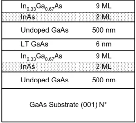
The specimens InAs-QDs were grown by the gas-source molecular beam epitaxy in the Stranski-Krastanov growth mode on an n+-doped GaAs (100) substrate. The alternating beam epitaxial technique and the overgrowth InGaAs layer method as well as the low growth rate of InAs-QD layer were employed. A schematic diagram of the QD structures is shown in Fig. 1.
GaAs Substrate (001) N+ Undoped GaAs 500 nm InAs 2 ML In0.33Ga0.67As 9 ML LT GaAs 6 nm Undoped GaAs 500 nm InAs 2 ML In0.33Ga0.67As 9 ML
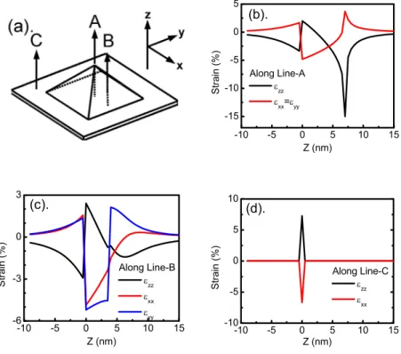
We consider an InAs pyramid QD (Fig. 2(a)) on a thin InAs layer within GaAs capped layer. The strain distribution can be discussed with linescans along the z direction at different positions of the xy plane. In Fig. 2(a), line A goes through the top of the pyramid, the line B intersects the dot at one half of the base length in [100] direction from the center, and line C is far away from the QD pyramid to display the strain in the wetting layer. Fig. 2(b). to (d) illustrate linescan of the strain tensor elements along line A, B, and C, respectively. In these figures, the solid line denotes εzz, the dashed line εxx, and the dotted line εyy. For line A and B, at the bottom of QD, εxx and εyy
is expected to be negative, because the lattice constant of InAs is longer than that of GaAs. But, this situation is not always hold as z position moving toward the top of QD. We could found that, near the top, they rapidly vary and finally change their sign to become positive. This happens because at the very top only small forces act on the QD in the xy plane, but the GaAs barrier compresses the pyramid mainly from the sides along the z direction, imposing tensile strain components in the xy plane [5]. Besides, the strains penetrate into the GaAs material. This will significantly affect the formation of vertical stacked QD structures [8].
-10 -5 0 5 10 15 -15 -10 -5 0 5 (b). Along Line-A εzz εxx=εyy Strain (%) Z (nm) -10 -5 0 5 10 15 -6 -3 0 3 (c). St rain (%) Z (nm) Along Line-B εzz εxx εyy -10 -5 0 5 10 15 -10 -5 0 5 10 (d). Along Line-C εzz εxx Strai n (%) Z (nm)
Fig. 2 (a). Schmatic drawing of pyramid geometry. Strain distribution along (b). Line A (c). Line B (d). Line C.
RESULTS AND DISCUSSION
The surface morphology of the sample was examined with field-emission scanning electron microscopy (FE-SEM) in the ambient environment. The density of QDs (SAQD) was about
7.64*1010 cm-2. Besides, the QDs sample was also measured with an atomic force microscope (AFM). The average base length and height of QD are 30 nm and 6 nm, respectively.
We performed the temperature-dependent PL experiments with low pumping power density. Because of low pumping power density, the contribution of emission of excited states could be neglected in PL spectrum. Thus, the lineshape reflects the distribution of QD size.
4 0.9 1.0 1.1 1.2 0 2 4 6 300 K 200 K 150 K 100 K 50 K 25 K 12 K No rma liz ed PL I nt ens ity (a rb . unit) E (eV) 0 100 200 300 0.94 0.96 0.98 1.00 1.02 PL P eak En ergy (eV) T (K)
Fig. 3 (a).Low pumping PL spectra of sample SAQD. (b). The PL peak energy as function of temperature.
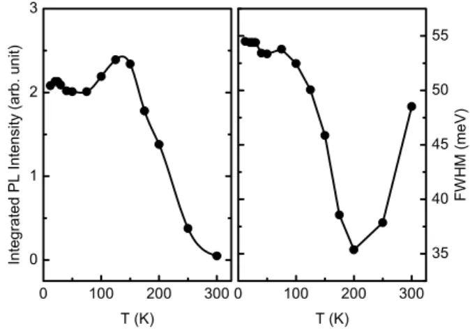
The FWHM of PL spectra (displayed in Fig. 4) almost keeps constant from 12 K to 100 K. As the temperature above 100 K, an unusual relationship is observed, which the FWHM decrease with temperature up to 200 K. In previous literature, this behavior has been explained with thermionic emission and repopulation process [9]. At low temperature, the PL lineshape of QDs is determined by the inhomogeneous distribution of QD size. Therefore, PL spectrum arises from the sum of emission of different dot sizes. When the temperature increases, the carriers will be thermalized in the quantum dots. The thermalized carriers can transfer to nearby potential local minimum, for example wetting layer. After this procedure, those carriers repopulate to the QDs, which are not filled. Because of Gaussian distribution of dot sizes, the repopulation process will occur more frequently for predominant QD sizes. Thus, the FWHM of PL spectrum is expected to be reduced, and we can obtain a narrower FWHM with increasing temperature. When the temperature is high enough (above 200 K in our results), the effect of electron-phonon scattering becomes a dominant contribution and FWHM increases with temperature increasing.
0 100 200 300 0 1 2 3 Integra ted PL Intens ity ( arb . un it) T (K) 0 100 200 300 35 40 45 50 55 FW HM (me V ) T (K)
Fig. 4 The integrated intensity and FWHM of PL spectra for sample SAQD.
experiments. PR spectra at temperature 20 K are displayed in the Fig. 5. In order to determine accurately and correctly the material parameters of the QDs sample from the PR spectra, the following procedures were done. (1). Using a Kramers–Kronig transformation technique, we could calculate the modulus of the PR spectrum. This process will remove the phase detail of the spectrum. It is very helpful to determine the transition energies of the optical features. (2). These energies were refined by fitting the PR spectra with the first derivative Gaussian function form. The |PR| spectrum of sample SAQD at 20 K is displayed in Fig. 5. There are four Gaussain-like
lineshapes in the spectrum. These peak values of Gaussian function are marked by arrows. Then, using these values as initial guess, we perform least square fitting for the PR spectra. The fitted energies of the optical transitions are marked with arrows and labeled alphabetically (A to E) from low to high energies. Five energy features were observed and the fitted energies and the broadening parameters or linewidths (Г) were listed in Table 1. The transition energy feature A located at 1.026 eV with a linewidth of 31 meV originates from the ground state transition of the InAs QDs. The features marked B, C, D, and E come from the optical transitions of the excited states of the InAs QDs. Fig. 5 displays also the high-pumping PL spectrum of the optical transitions of the ground state (E0) and the first two excited states (E1 and E2). Similar PL results
of the excited state levels were observed and reported in literature [10]. The peak energy values are consistent with the PR fitted results.
Table 1 Fitted results of PR spectra of InAs QD samples. The unit of energy E and broadening parameter Γ are eV and meV, respectively.
Energy Features A B C D E F G H E 1.026 1.114 1.193 1.286 1.354 1.458 1.506 1.516 20 K Γ 31 15 18 14 12 25 9 4 E 1.018 1.084 1.170 1.252 1.337 --- 1.507 1.515 100 K Γ 20 17 18 15 14 --- 4 3 E 0.973 1.047 1.129 1.199 1.275 1.415 1.462 1.484 200 K Γ 24 20 23 19 13 24 3 3 ↓ ↓ ↓ ↓ ↓ A B C D E -1 0 1 2 20 K ∆ R/R x 10 5 (a.u.) 0.9 1.0 1.1 1.2 1.3 1.4 |P R| E (eV) ↓ ↓ ↓ ↓ ↓ A B C D E ↓ ↓ ↓ E0 E 1 E2 -1 0 1 2 20 K ∆R/ R x 10 5 (a .u .) 0.9 1.0 1.1 1.2 1.3 1.40 2 4 6 8 10 PL In te n si ty x 1 0 2 (a .u .) E (eV)
6
The interlevel spacings between the energy features (A to E) in Fig. 5 are nearly equal (75-80 meV) and are higher than those reported in literatures [11, 12]. The reason why nearly equal spacing in energy occurs may be because spatially lateral (in-plane) simple harmonic potentials exist in the QDs as reported in literature [13]. We calculated the energy levels in the QDs with a lateral harmonic potential. In calculations, we used an effective diameter of 36.0 nm, which is slightly larger than the base diameter of 30 nm measured by field-emission scanning electron microscopy. For InAs, the effective masses of the electron and the heavy hole used in our calculations were 0.04 and 0.51, respectively. The interlevel spacing in energy was estimated to be 79.4 meV and is in good agreement with our experimental results.
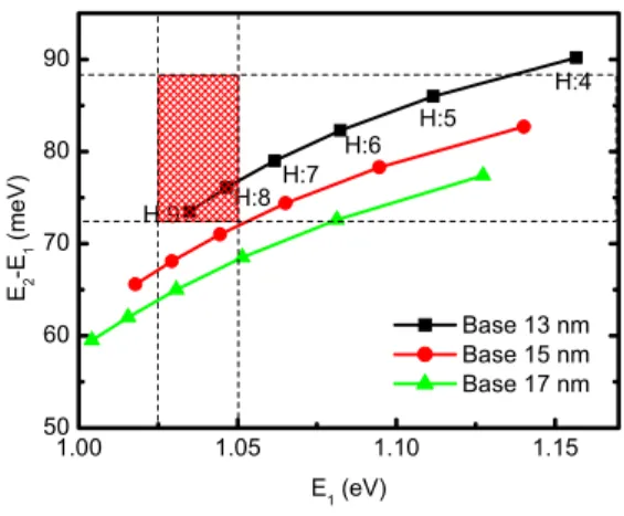
In order to explore the origin of the optical transitions and to predicate the optical properties, it is necessary to perform more rigid theoretical calculation for QD structures. We carried out the theoretical calculation of 8x8 Hamiltonian model by Orthogonal Periodic Function method including strain effects for pyramidal QDs (displayed in Fig. 6). The square (circle, triangle) symbols are obtained by assuming the base length is 13 nm (15, 17 nm). Each point with same symbols is the results of varying the QD height with same base length. The height varies from 4 nm to 9 nm. The cross-line area is determined by following descriptions. (1). Horizontal limitation: The lower limitation is the fitted results of PR and PL spectrum (E1 at 1.026 eV). The
upper limitation is the ground state energy plus binding energy of ground state (about 20-25 meV
[5]). (2). Vertical limitation: The upper boundary is obtained from the energy difference of
experimental results (88 meV). Then, according to Ref. 14, the ratio of binding energy of ground and first excited state is 0.25 for very large microcrystallites and about 0.3 for small microcrystallites. So, take binding energy into consideration, the energy difference should be corrected by about -15 meV.
1.00 1.05 1.10 1.15 50 60 70 80 90 H:5 H:4 H:6 H:7 H:8 H:9 E2 -E1 (m eV ) E1 (eV) Base 13 nm Base 15 nm Base 17 nm
Fig. 6 The calculated energy difference between ground and first excited state as a function of ground state energy.
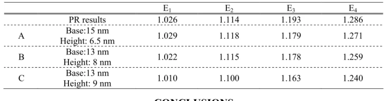
We summarize the calculated results, which points are located in the cross-line area, in the Table 2. Compared experimental results with these three cases, the results of case A are in good agreement with experiments, not only for E1 and E2. Even for higher excited states E3 and E4, the
nm and 6 nm measured by FESEM and AFM. It is also consistent with our calculation.
Table 2 Summary of calculation and compared with the experimental results.
E1 E2 E3 E4 PR results 1.026 1.114 1.193 1.286 A Height: 6.5 nm Base:15 nm 1.029 1.118 1.179 1.271 B Height: 8 nm Base:13 nm 1.022 1.115 1.178 1.259 C Height: 9 nm Base:13 nm 1.010 1.100 1.163 1.240 CONCLUSIONS
We have characterized the optical properties of the InAs/GaAs QD structures by the PR and the PL spectroscopies at various temperatures. Detailed energy features from well-fitted PR spectra were analyzed. Signals from a ground state, four excited states were identified and discussed. From results of PL experiments, we could find that the linewidth decreased as temperature increased to 100 K, due to the repopulation of thermalized carriers. Energy features of the PR spectra originating from QDs were characterized. The fitted results show that the ineterlevel spacing of each optical transition is almost equal. To explain this effect, calculation of in-plane parabolic potential model is carried out. The energy spacing of calculated results is consistent with PR results, under the assumption of diameter 36 nm, which is slight larger than base length of QD measured by AFM and FESEM. Moreover, we also performed the theoretical calculations of 8x8 Hamiltonian model including the effect of strain to calculated the transition energies for pyramidal QD shape. After correction of binding energy, the calculated results are in good agreement with the experimental results.
REFERENCES
1 J.-Y. Marzin, J.-M. Gérard, A. Izraë, and D. Barrier, Phys. Rev. Lett. 73, 716 (1994).
2 N. N. Ledentsov, D. Bimberg, V. M. Ustinov, Zh. I. Alferov, and J. A. Lott, Jpn. J. Appl. Phys. 41, 949 (2002).
3 M. V. Maximov, L. V. Asryan, Y. M. Shernyakov, A. F. Tsatsul’nikov, I. N. Kaiander, V. V. Nikolaev, A. R. Kovsh,
S. S. Mikhrin, V. M. Ustinov, A. E. Zhukov, Zh. I. Alferov, N. N. Ledentsov, and D. Bimberg, IEEE J. Quantum Electron. 37, 676 (2001).
4 V. Ryzhii, Semicond. Sci. Technol. 11, 759 (1996).
5 M. Grundmann, O. Stier, and D. Bimberg, Phys. Rev. B 52, 11969 (1995).
6 M. A. Cusack, P. R. Briddon, and M. Jaros, Phys. Rev. B 54, R2300 (1996).
7 C. Pryor, M.-E. Pistol, and L. Samuelson, Phys. Rev. B 56, 10404 (1997).
8 A. A. Darhuber, V. Holy, J. Stangl, G. Bauer, A. Krost, F. Heinrichsdroff, M. Grundmann, D. Bimberg, V. M.
Ustinov, P. S. Kop’ev, A. O. Kosogov, and P. Werner, Appl. Phys. Lett. 70, 955 (1997).
9 Y. T. Dai, J. C. Fan, Y. F. Chen, R. M. Lin, S. C. Lee, and H. H. Lin, J. Appl. Phys. 82, 4489 (1997).
10 K. H. Schmidt, G. Medeiros-Ribeiro, M. Oestreich, and P. M. Petroff, Phys. Rev. B 54, 11346 (1996).
11 D. L. Huffaker, G. Park, Z. Zou, O. B. Shchekin, and D. G. Deppe, Appl. Phys. Lett. 73, 2564 (1998).
12 J. J. Finley, M. Skalitz, M. Arzberger, A. Zrenner, G. Böhm, and G. Abstreiter, Appl. Phys. Lett. 73, 2618 (1998).
13 A. Wojs, P. Hawrylak, S. Fafard, L. Jacak, Phys. Rev. B 54, 5604 (1996).