Emission dynamics of InAs self-assembled quantum dots with different cap layer structures
This article has been downloaded from IOPscience. Please scroll down to see the full text article.
2008 Semicond. Sci. Technol. 23 075044
(http://iopscience.iop.org/0268-1242/23/7/075044)
Download details:
IP Address: 140.112.113.225
The article was downloaded on 06/02/2009 at 03:40
Please note that terms and conditions apply.
The Table of Contents and more related content is available HOME | SEARCH | PACS & MSC | JOURNALS | ABOUT | CONTACT US
Semicond. Sci. Technol. 23 (2008) 075044 (5pp) doi:10.1088/0268-1242/23/7/075044
Emission dynamics of InAs self-assembled
quantum dots with different cap layer
structures
Ling Min Kong
1, Zhe Chuan Feng
2, Zheng Yun Wu
3and Weijie Lu
41Department of Physics, Zhejiang Ocean University, Zhoushan 316000, People’s Republic of China 2Institute of Photonics and Optoelectronics, and Department of Electrical Engineering,
National Taiwan University, Taipei, 106-17 Taiwan, Republic of China
3Department of Physics, Xiamen University, Xiamen 361005, People’s Republic of China 4Department of Chemistry, Fisk University, Nashville, TN 37208, USA
E-mail:[email protected]
Received 1 February 2008, in final form 1 May 2008 Published 4 June 2008
Online atstacks.iop.org/SST/23/075044
Abstract
The emission dynamics properties of self-assembled InAs quantum dots with different cap layers are investigated by steady-state and time-resolved photoluminescence (PL). The uniformity of the dots can be improved by the proper cap layer structure. It is found that the InGaAs and InAlAs combination cap layer structure could more effectively release the strain in QDs, suppress the indium segregation, enhance the confinement effect on carriers and reduce the thermally induced carrier escape from QDs. This has led to QDs with narrower emission, above 1.3 µm, and to improved temperature stability of PL intensity and has resulted in an increase of the PL decay time to 10 ns at 160 K.
(Some figures in this article are in colour only in the electronic version)
1. Introduction
Recently, self-assembled quantum dots (QDs), with the effect of three-dimensional size confinement, have attracted extensive research interest due to their unique physical properties and potential device applications [1–7]. However, there are still many technical barriers to overcome to fully utilize their potential applications. As to the laser diode application from QDs, the energy gap between the ground state and the first excited state must be greater than the value of
kT, and inhomogeneous broadening in the photoluminescence
(PL) should be small, which requires suitable QD size and uniform distribution of QDs. However, the stochastic nature of the QDs makes it difficult to obtain dots with uniformity in both their size and spatial distribution, which seriously limits their potential device application. The change in the band discontinuity between QDs and confining layers is a useful way to improve QDs quality [5–12].
Generally, it is found that in the InAs/GaAs structures with InGaAs capping layer, the emission energy of the InAs quantum dots (QDs) shows a red-shift with the increase of In content in the InxGa1−xAs capping layer up to x = 0.3
[5,8,9,10]. If the InGaAs cap layer has higher In composition, then it will have higher compressive strain with respect to GaAs, lowering the emission energy [9]. Mukai et al [5] considered that the lattice-constant variation will provide the most likely explanation for the temperature insensitive emission energy by the overgrowth of InGaAs layer. They found that the emission energy shift over 150 K was almost negligible when x= 0.25 and 0.3, and the shift between 4.2 and 200 K was less than half that of bulk GaAs when x = 0.3. However, Wang et al [8] considered that when x > 0.1, larger x resulted in a larger PL linewidth, and they obtained the maximum integrated PL intensity for x= 0.2. Considering other effects such as the PL linewidth and integrated intensity, the x= 0.2 InxGa1−xAs capping layer shows the best results
for the fabrication of long wavelength InAs QDs lasers. Furthermore, to achieve long wavelength and high quality emission, InAs QDs with InAlAs and InGaAs combination cap layers (CCL) were fabricated [10–13]. Compared to the traditional InAs QDs, this structure with CCL has attractive fundamental properties, such as red-shift of the emission [10,11,13], reduction of the PL line width [10, 12], larger
Semicond. Sci. Technol. 23 (2008) 075044 L M Kong et al
energy separation between the ground and first excited states [10, 11, 13] and enhancement of the PL intensity [10–13]. These interesting properties can be attributed to the fact that the combination cap layer can suppress the segregation of indium component and then increase the height of the dots [4,10–13]. Even though studies concerning the carrier transfer mechanisms and corresponding transit times in such systems are necessary for fabricating high-efficiency optoelectronic and electronic devices, however, up to now, very few works have been done on the effects of combination cap layers by time-resolved photoluminescence (TRPL). TRPL is a useful technique, which we have recently employed to study the dynamics properties of other types of QDs [6,14]. In this paper, we have investigated the carrier dynamics by the steady state and TRPL in InAs quantum dots capped with different layers, which can help to penetratingly understand the effects of InAlAs and InGaAs combination cap layers on the structures and optical properties of InAs QDs.
2. Experimental section
Three types of InAs/GaAs QD samples have been prepared with different cap layer structures. All samples were grown on semi-insulating GaAs (1 0 0) substrates by a VG V80 molecular beam epitaxy (MBE) system. After a 500 nm GaAs buffer (600 ◦C) and a 20 nm GaAs layer (510◦C), a 2.5 monolayer (ML) of InAs was grown to form a random distribution of QDs. The self-assembled QDs layers were then capped by different cap layers, 1 nm In0.3Al0.7As and 3 nm In0.2Ga0.8As combination layer for sample S1 and 3 nm In0.2Ga0.8As for sample S2, separately. Finally a 60 nm GaAs layer was grown on the top. In addition, a comparative sample S3 was prepared in the same way except that it has only the 60 nm GaAs cap layer without InGaAs or InAlAs layer between the QDs layer and the 60 nm GaAs cap.
Steady-state PL and TRPL were measured in the temperature (T) range of 10–300 K. Time-correlated single photon counting system measurements were performed with the help of a 638 nm semiconductor laser delivering 100 ps pulses at 20 MHz and a Hamamatsu R5509-72 near infrared (NIR) photomultiplier tube (PMT) [6,14].
3. Results and discussion
3.1. Photoluminescence measurement
The normalized PL spectra of three QD samples at 10 K are shown in figure1. Luminescence features from the cap layer do not appear, which indicates that the carriers generated in the cap layer can efficiently be injected into InAs QDs. The PL peak energies of samples S1, S2 and S3 are at 1.003 eV, 1.052 eV and 1.062 eV, respectively. It shows a 10 meV red-shift from the sample S3 with the GaAs cap to S2 with the InGaAs cap, and a further 49 meV red-shift from the sample S2 to S1 with the InAlAs and InGaAs combination cap layer (CCL). Obviously, PL shows much more red-shift for samples with the CCL structure. The full-width at half-maximum (FWHM) values are 35 meV for S2, 37 meV for
0.95 1.00 1.05 1.10 1.15 1.20 1.25 0.0 0.2 0.4 0.6 0.8 1.0 0.90 0.95 1.00 (eV) S1 Norm ali zed PL int ensit y (ar b .u.)
Photon energy (eV) S1
S2 S3 300 K
Figure 1. Normalized PL spectra of samples S1, S2 and S3 at 10 K;
the inset is the PL spectrum of sample S1 at 300 K.
S3, but only 26 meV for S1, respectively. This fact indicates that the CCL can greatly improve the PL characteristics of the QDs.
Our experimental results can be explained from the strain analysis. It is understood that the strain forces affect the PL peak and FWHM of the QDs mostly, and they are influenced by the cap layer structure [4]. The strain forces between QDs and the buffer layer are directly proportional to the square of lattice mismatch. With the reduction in the lattice mismatch, strain forces drop down rapidly. For sample S1, the InGaAs and InAlAs CCL may enhance the paths of strain release, which increase the range of InAs deposition dose. During the growth process of CCL, indium atoms in InGaAs and aluminum atoms in InAlAs can retard the diffusion of indium and gallium atoms between InAs QDs and GaAs barrier layers, which may commendably preserve the uniform size distribution of InAs QDs [1,2]. This phenomenon reduces the strain force and probably increases the QDs height. The reduction in strain among InAs QDs results in a strong red-shift of PL. It must be noted that the increase of confinement potential for InAlAs may cause the increase of the ground-state energy. However, this effect is not obvious, as compared to the red-shift from the strain reduction. As shown in the inset of figure1, the emission wavelength of sample S1 reaches 0.93 eV, i.e. 1.33 µm at 300 K.
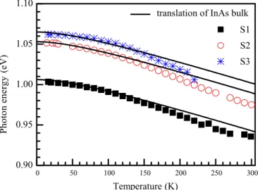
Temperature-dependent PL measurements were measured in 10–300 K for these three samples. Figure 2 shows the temperature dependence of PL peak energy for three samples. PL signals from S3, the QDs sample with the GaAs cap but without the InGaAs or InAlAs layer, were very weak above 230 K, which were not recorded. This also provides the evidence that the InGaAs or InGaAs/InAlAs combined layer structure can improve the luminescence characteristics of InAs QDs.
Three solid lines (starting from 1.065, 1.053 and 1.006 eV, respectively) are the translation of the InAs gap (0.417 eV) fitted by the Varshini formula for guides of eye [2]. The overall behavior is similar for these three samples. Due to the localization effects, the PL peak energies of the three samples are more or less a constant below 30 K [6]. The PL peak energy of the QDs decreases as temperature increases within
Figure 2. Temperature dependence of PL peak energy for three
samples; the solid lines are the translations of InAs gap fitted by the Varshini formula; the translations between these three lines and InAs gap (0.417 eV) are 0.648, 0.636 and 0.589 eV, respectively.
30–120 K, in accordance with the Varshini formula and similar to the behavior of InAs bulk material.
But beyond 120 K, the PL peak energies of three samples were deviated from Varshini-shape curves, in comparison with the energies of InAs bulk. The amounts of these deviations gradually increase with an increase of temperature beyond 120 K. This is a characteristic feature of self-assembled QDs grown by the Stranski–Krastanow (SK) mode [10]. This behavior indicates an increase in the rate of carrier migration among different QDs, especially the migration rate from the small QDs with higher energy level to larger QDs with lower energy level, resulting in a fast red-shift of PL wavelength [2]. It is obvious that as temperature increases, sample S3 has the largest value of red-shift, while sample S1 has the least one. From 120–220 K, the red-shifts of InAs bulk, S1, S2 and S3 are 27 meV, 31 meV, 37 meV and 42 meV, respectively. The above phenomena mean that S1 has better thermal stability for the CCL.
The spectrally integrated PL signal allows us to monitor the quenching of the emission strength with temperature, as displayed in figure3. As done in figure1, the PL intensities of three samples at 10 K are normalized to 1 for comparative analysis. The integrated PL intensity can be fitted by the formula
I (T )= I0/(1 + C0exp(−Ea/kT )), (1) where Ea is the activation energy, I0 is a constant, k is the Boltzmann constant and C0 contains ratios of optical-collection efficiencies and effective degeneracies between the unbound and bound states [15]. The ratios of PL integrated intensity of 14 K and that of 230 K are 143, 318 and 3440 for samples S1, S2 and S3 separately. Sample S1 could be detected strong luminescent signals at room temperature, while sample S3 could not be detected luminescent signals above 230 K, as mentioned before. Fitting the data in figure 3 with the formula (1), we obtain the least C0 of 1595 for sample S1 (34 030 and 106 900 for S2 and S3), and the smaller value of
0 20 40 60 80 100 S1 (a) (b) (c) P L in teg rated in ten sit y (arb . u .) S2 1000/T (K-1) S3 C0=1.3
Figure 3. Temperature dependence of the integrated intensities for
three InAs QDs samples; the solid lines were fitted by formula (1).
C0means the higher ratios of optical-collection efficiencies, i.e. with better property. It is interesting that the integrated PL intensity of S3 has an obvious variation of decrease–increase– decrease process as temperature rises. For the sample S3, we also obtain the activation energy of 4 meV and C0 of 1.3 from the data of figure 3(c) in the range of 10–60 K, suggesting that the dots have a common activation energy at low temperature, which may originate from the carrier localization effects caused by the small barriers for the component and interface fluctuation around the dots. The above phenomena indicate that the CCL can significantly improve the temperature stability of PL intensity.
At room temperature, no obvious PL signals can be detected from sample S3 under the same measurement conditions as for samples S1 and S2. At the low temperatures of 10–230 K, PL intensities of S3 were more than one order weaker than that of S1 and S2 at each corresponding measurement temperature . The enhancement of PL intensities from InAs QDs with a CCL layered structure might also be due to the strain release of the combined cap layer structures, similar to the analysis in section3.1. More penetrating studies on this and other interesting phenomena observed in the paper are required.
3.2. Time-resolved PL spectra
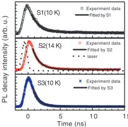
It is crucial to understand the dynamic process of carrier relaxation for the development of QD lasers. In order to study the effects of CCL on dynamic information of carriers, time-resolved photoluminescence measurements were performed for these three QD samples in a wide temperature range. Figure 4 shows PL decay spectra of the three samples at low temperatures and decay curve fitting results. Each TRPL spectrum can be fitted with a single exponential consisting of an individual PL decay time, τ .
Semicond. Sci. Technol. 23 (2008) 075044 L M Kong et al 0 5 1 0 1 5 Time (ns) PL deca y intensity (arb . u.) Experiment data Fitted by S2 laser S2(14 K) Experiment data Fitted by S1 S1(10 K) Experiment data Fitted by S3 S3(10 K)
Figure 4. PL decay spectra and decay curve fittings of three
InAs-QDs samples at a low temperature of 10 K or 14 K.
Figure 5. PL decay time of the three samples at different
temperatures.
Figure5exhibits the obtained PL decay times, τ , versus
T for these three samples at 10–300 K. As shown, the overall
trend is similar for three InAs QDs: the PL decay time is almost constant below 30 K, rises gradually below 80–100 K, further rises and reaches a maximum value, the critical temperature TC, at a middle temperature, and then drops at higher temperature. However, the detailed τ –T relations for three samples differ from each other. In particular, the values of TCand τ data are quite different among them. TCvalues of 180 K, 160 K and 130 K are shown for S1, S2 and S3, respectively.
The corresponding temperature for PL decay time of S1 being a constant is much lower than those previously reported for InAs QDs in a GaAs matrix [16,17,20–25]. This fact may imply that carriers generated in the cap layer can be efficiently injected into InAs QDs with smaller interface barrier. The maximum PL decay time of sample S1 observed is 9.66 ns, which is larger than that of other two samples and previously reported values [16–20]. Karachinsky et al [21] considered that, for larger QD diameters, the piezoelectric effect leads the electron and hole wavefunction expanding in different directions and becoming more elongated, hence reducing the overlap integral, and results in a longer lifetime. Langbein
et al [22] believed that increasing quantum confinement may result in a longer lifetime for smaller in-plane extension of the exciton wavefunctions. Our results show that the increase of
the QDs height and the quantum confinement from the CCL should be the most important reason for the long lifetime of S1.
It should emphasize that time decay PL spectra represent the composite decay rates of PL from QD materials. Carrier recombination can be simply described by the equations:
d(N (t)) dt = − N (t ) τ0 , (2) d(N (t) dt = − N (t ) τt = g −N (t ) τ0 , (3)
where τ0is the PL decay time at lower temperature, N(t) is the number of total carriers in QDs, τtis the PL decay time
at higher temperature, and g is the rate of additional carrier migration from the barrier region to QDs for the temperature effect. Equation (2) describes a decay process with a constant decay parameter, while equation (3) describes the process with non-constant decays. At lower (<30 K), dynamic processes, such as non-radiative recombination, thermal excitation and migration of carriers are irrelevant. Therefore, PL decay spectra mainly represent the rate of radiative recombination. The value of g can be neglected, so the PL decay time is more or less a constant. As the temperature increases above 30 K, the value of g cannot be neglected. From equations (2) and (3), we can deduce that τt is larger than τ0. This can partially explain the increase of the decay time for samples S2 and S3 below about 100 K. But as for S1, PL intensity just decreases with temperature. There are also other mechanisms of enhancing the decay time, such as the thermally-induced carriers redistribution among the QDs with different tunneling rates for the electrons and the holes [7,16,18], the thermally-induced population of dark excitons [4 19, 23] and excited states [20–24,26] and the thermally-induced reduction of the effective oscillator by the carrier expansion, while the non-radiative recombination suppresses the lifetime [16,17].
From the above analysis, it can be considered that the larger TCmeans a lesser effect of non-radiative recombination. Obviously, TCof sample S1 is much larger than that of the other two samples, and also larger than that reported in [16] (150 K), [20] (150 K), [26] (170 K) and [24] (no TCwithin the experimental error). Further, the decay time remains rather large up to RT for sample S1, demonstrating the high structural quality of the embedded QDs [20]. The high values of TC and the decay time observed in the high temperature regime indicate that in the CCL structure barriers tend to enhance the confinement effect on the carriers, inhibit thermal escape of carriers from the dots [26] and reduce non-radiative recombination.
4. Conclusion
We have experimentally investigated time-resolved photoluminescence of InAs quantum dots capped with different cap layers. It is observed that by capping with a combination cap layer, the QDs emit longer and narrower emission (above 1.3 µm at room temperature). We attribute the results to effective strain release in the QDs
due to CCL. At the same time, temperature stability of the PL efficiency and decay time was enhanced for the higher potential barrier of CCL layer than that of the InGaAs layer. More carriers migrating to the QDs from barriers and the wetting layer, and the thermally induced reduction of the effective oscillator by carrier expansion among the different QDs, dark excitons and excited states are the main reasons for the PL decay time increasing with temperature. At higher temperatures, thermal emission and the non-radiative recombination reduce the PL decay time.
Acknowledgments
This work was supported partially by the science projects of Zhejiang Ocean University, grant nos. 11064100107 and 210650049, and at National Taiwan University by funds of NSC 95-2221-E-002-118- and NSC96-2221-E002-166.
References
[1] Marzin J Y and Bastard G 1994 Solid State Commun.92 437 [2] Sanguinetti S, Henini M, Grassi Alessi M, Capizzi M,
Frigeri P and Franchi S 1999 Phys. Rev. B60 8276 [3] Arpatzanis N, Tassis D H, Dimitriadis C A, Charitidis C,
Song J D, Choi W J and Lee J I 2007 Semicond. Sci. Technol.22 1086
[4] Saito H, Nishi K and Sugou S 1998 Appl. Phys. Lett.73 2742 [5] Mukai K and Sugawara M 1999 Appl. Phys. Lett.74 3963 [6] Kong L M, Wu Z Y, Feng Z C and Ferguson I T 2007 J. Appl.
Phys.101 126101
[7] Nishi K, Saito H, Sugou S and Lee J S 1999 Appl. Phys. Lett. 74 1111
[8] Wang X D, Niu Z C, Feng S L and Miao Z H 2001 J. Cryst. Growth223 363
[9] Tarasov G G, Mazur Yu I, Zhuchenko Z Ya, Maaßdorf A, Nickel D, Tomm J W, Kissel H, Walther C and Masselink W T 2000 J. Appl. Phys.88 7162
[10] Liu H Y, Tey C M, Sellers I R, Badcock T J, Mowbray D J, Skolnick M S, Beanland R, Hopkinson M and Cullis A G 2005 J. Appl. Phys.98 083516
[11] Chang K P, Yang S L, Chuu D S, Hsiao R S, Chen J F, Wei L, Wang J S and Chi J Y 2005 J. Appl. Phys.97 083511 [12] Liu W S and Chyi J I 2005 J. Appl. Phys.97 024312
[13] Fang Z D, Gong Z, Miao Z H, Kong L M, Xu X H, Ni H Q and Niu Z C 2004 J. Phys. D: Appl. Phys.37 1012
[14] Kong L M, Cai J F, Wu Z Y, Gong Z, Niu Z C and Feng Z C 2006 Thin Solid Films498 188
[15] Kim J C, Rho H, Smith L M, Jackson H E, Lee S, Dobrowolska M and Furdyna J K 1999 Appl. Phys. Lett. 75 214
[16] Paillard M, Marie X, Vanelle E, Amand T, Kalevich V K, Kovsh A R, Zhukov A E and Ustinov V M 2000 Appl. Phys. Lett.76 76
[17] Mu X D, Ding Y J, Ooi B S and Hopkinson M 2006 Appl. Phys. Lett.89 181924
[18] Yang W, Lowe-Webb R R, Lee H and Sercel P C 1997 Phys. Rev. B56 13314
[19] Boggess T F, Zhang L, Deppe D G, Huffaker D L and Cao C 2001 Appl. Phys. Lett.78 276
[20] Fiore A, Borri P, Langbein W, Hvam J M, Oesterle U, Houdr´e R, Stanley R P and Ilegems M 2000 Appl. Phys. Lett.763430
[21] Karachinsky Ya L, Pellegrini S, Buller G S, Shkolnik A S, Gordeev Yu N, Evtikhiev V P and Novikov V B 2004 Appl. Phys. Lett.84 7
[22] Langbein W, Borri P, Woggon U, Stavarache V, Reuter D and Wieck A D 2004 Phys. Rev. B70 033301
[23] Gurioli M, Vinattieri A, Zamfirescu M, Colocci M, Sanguinetti S and Richard N¨otzel 2006 Phys. Rev. B 73 085302
[24] Markus A, Fiore A, Gani`ere J D, Oesterle U, Chen J X, Deveaud B and Riechert H 2002 Appl. Phys. Lett. 80 911
[25] Shu G W, Wang C K, Wang J S, Shen J L, Hsiao R S, Chou W C, Chen J F, Lin T Y, Ko C H and Lai C M 2006 Nanotechnology17 5722
[26] Pulizzi F, Kent A J, Patan`e A, Eaves L and Henini M 2002 Appl. Phys. Lett.84 3046