348 IEEE ELECTRON DEVICE LETTERS, VOL. 22, NO. 7, JULY 2001
Post-Soft-Breakdown Characteristics of Deep
Submicron NMOSFETs with Ultrathin Gate Oxide
Min-Yu Tsai, Horng-Chih Lin, Member, IEEE, Da-Yuan Lee, and Tiao-Yuan Huang, Fellow, IEEE
Abstract—The impacts of soft-breakdown (SBD) on the
char-acteristics of deep sub-micron NMOSFETs were investigated. It is shown that the BD location plays a crucial role in the post-BD switching function of the device. When BD occurs at the channel, the turn-on behavior of the drain current would not be significantly affected, which is in strong contrast to the case of BD at the drain. Nevertheless, significant increase in gate current is observed in the off-state when the gate voltage is more negative than 1 V. Its origin is identified to be due to the action of two parasitic bipolar transistors formed after SBD occurrence at the channel.
Index Terms—Gate induced drain leakage, gate leakage,
para-sitic bipolar transistor, soft-breakdown.
I. INTRODUCTION
S
OFT-BREAKDOWN (SBD) events are frequently observed as oxide is thinner than 5 nm [1]–[7]. One interesting feature associated with this BD mode is that the device switching behavior may be retained even after its occurrence, in strong contrast to the case of conventional hard breakdown (HBD) [3]. In addition, impacts of SBD on device characteristics also depend on the BD location. For example, Pompl et al. [4] reported that, when SBD occurs within the gate/drain overlap region, gate induced drain leakage (GIDL) current will be increased. On the other hand, Wu et al. [5] observed that the gate leakage, rather than the GIDL, dominates the off-state drain current when BD is induced in the drain region. Their results also indicated that the device’s switching function could be destroyed, if BD occurs at the drain. In order to distinguish the disparity among different reports, we characterized the post-SBD characteristics of deep submicron n-channel devices in this study. Special attention was paid to the effects of BD location and their impacts on the device performance, especially the off-state leakage characteristics.II. EXPERIMENTAL
N-channel MOS transistors with n poly-Si gate were fab-ricated on 6-inch Si wafers. Nominal gate oxide thickness and
Manuscript received March 6, 2001; revised April 11, 2001. This work was supported by the National Science Council of Taiwan, R.O.C., under Contract NSC 89-2215-E-009-105. The review of this letter was arranged by Editor C.-P. Chang.
M.-Y. Tsai and D.-Y. Lee are with the Institute of Electronics, National Chiao Tung University, Hsinchu 300, Taiwan R.O.C.
H.-C. Lin is with the National Nano Device Laboratories, Hsinchu 300, Taiwan R.O.C. (e-mail: [email protected]).
T.-Y. Huang is with the Institute of Electronics, National Chiao Tung Uni-versity, Hsinchu 300, Taiwan R.O.C., and also with the National Nano Device Laboratories, Hsinchu 300, Taiwan R.O.C.
Publisher Item Identifier S 0741-3106(01)05792-5.
Fig. 1. Current–voltage characteristics of (a) a fresh device, and devices with first SBD event occurs (b) within the channel, and (c) at the drain. (V = 1:5 V). The arrow in (b) indicates the point where the substrate current flow reverses its direction.
channel length/width are 2.5 nm and 0.2/10 m, respectively. Electrical characterizations were performed using a HP-4156
TSAI et al.: POST-SOFT-BREAKDOWN CHARACTERISTICS OF DEEP SUBMICRON NMOSFETs WITH ULTRATHIN GATE OXIDE 349
Fig. 2. I –V characteristics of a device before and after BD occurs within the channel.
parameter analyzer. Some devices were stressed at room tem-perature under a gate bias of 4.5 V with all other terminals (i.e., source, drain, and substrate) grounded. Device character-istics before and after BD were measured and analyzed.
III. RESULTS ANDDISCUSSION
Occurrence of the first soft breakdown (SBD) event in oxide could be located at the drain, source, or the channel region of a device. In [5], it was shown that most BD events would be induced in the source/drain overlapped region for deep sub-mi-cron devices. In this work, similar trend was observed. Never-theless, we have indeed detected all these types of BD events. Fig. 1(a)–(c) show typical characteristics of fresh device, BD at the channel, and BD at the drain, respectively. In Fig. 1(b), the substrate current changes its sign (i.e., flow direction) at V (highlighted by the arrow in the figure), in-dicating that the BD location is within the channel region. In Fig. 1(c), BD occurs at the drain, since coincides with in the off-state. As can be seen in Fig. 1, when BD occurs at the channel, the subthreshold and on-state characteristics of the drain current are not significantly affected. In contrast, BD at the drain would increase dramatically the off-state drain current, se-verely degrading the device switching behavior [5].
For devices with BD at the channel, as mentioned above, the tun-on behaviors will not be significantly affected. When the off-state characteristics after BD are compared with those of the fresh devices, however, it is interesting to find that two regions, one in the range from V and the other with V, show increased , as illustrated in Fig. 2. The increase in the range from V is also observed before BD is induced. By carefully analyzing and characteristics in the range of interest as a function of stressing time (data not shown), it is concluded that the increase after stressing is mainly contributed by the increased
. The other contribution is from the gate leakage, albeit minor. One possible explanation is that the stressing would in-crease the interface-state density, and thus enhance the trap-as-sisted gate-induced drain leakage (GIDL), , and the stress-induced leakage currents (SILC), [8].
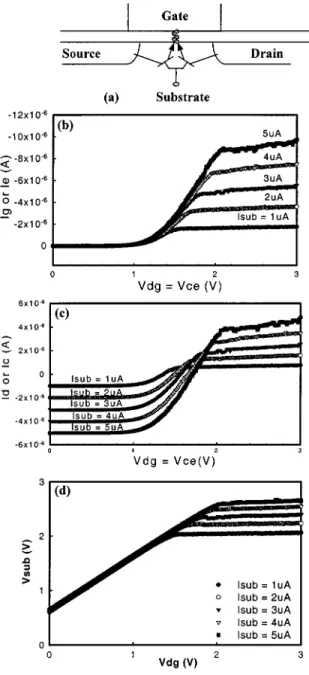
Fig. 3. (a) Formation of two parasitic bipolar junction transistors (BJTs) after BD occurs within the channel. Results in (b)–(d) are characteristics of the drain-side BJT characterized with common-emitter scheme (i.e.,V = 0 and source floating). The device is the same as that shown on Fig. 1(b).
On the other hand, the increase in after SBD for V is believed to be due to the action of the parasitic bipolar transistors formed after SBD. When BD occurs at the channel, two parasitic npn bipolar transistors would be formed in the substrate, as shown in Fig. 3(a). The two transistors share a common base (i.e., substrate) and a common emitter (i.e., n poly-Si), but with separate collectors (i.e., drain and source, respectively). In this work, the action of the bipolar transistor is clearly demonstrated. One example is shown in Fig. 3. Here, only the drain-side bipolar transistor was characterized by floating the source during measurement. Fig. 3(b) and (c) show (or ) and (or ) as a function of (or ), respectively. The measurements were performed with the common-emitter configuration, i.e., . Base (substrate) current is used as the input parameter. We can see that the
350 IEEE ELECTRON DEVICE LETTERS, VOL. 22, NO. 7, JULY 2001
device is essentially operating in the saturation region when is smaller than 2 V, as evidenced by the results shown in Fig. 3(d) in which is larger than both and . This indicates that both the emitter-base and the base-collector junctions are forward-biased. On the other hand, the device will be operating in the active mode when is larger than 2 V, so the base-collector junction becomes reverse-biased. The large offset in the axis is mainly ascribed to the large parasitic emitter resistance, due to the small area of BD spot [9].
For the current–voltage characteristics of the device with BD spot located within the channel region [Figs. 1(b) and Fig. 2], the parasitic bipolar transistors would be triggered into the ac-tive mode in the negaac-tive gate voltage region when is large enough. As a result, the drain current would be amplified, re-sulting in the increase in the large negative region, as ob-served.
Note that the enhanced GIDL phenomenon after the occur-rence of SBD reported in [4] is not detected in this work. The enhanced GIDL could be observed only in the small range before the SBD is induced. This discrepancy is presumably re-lated to the thicker gate oxide used in the previous work [4] (3 and 4 nm), and implies that the SBD mechanism could be dif-ferent as oxide is scaled below 3 nm.
IV. CONCLUSIONS
In summary, we have investigated the post-SBD characteris-tics of n-channel MOSFETs with 2.5 nm-thick gate oxide. Sev-eral important findings are obtained. 1) The BD location plays an important role in affecting the switching function of the de-vice. If BD occurs at the drain, significant leakage form the gate would destroy the normal operation of the device. 2) During
stressing, enhanced GIDL and SILC gate currents caused by the generated interface states account for the increased drain leakage in the small negative range. 3) When BD occurs in the channel, large increase in for V is identified to be due to the action of the parasitic npn transistors.
REFERENCES
[1] F. Crupi, R. Degraeve, G. Groesenekenm, T. Nigam, and H. E. Maes, “On the properties of the gate and substrate current after soft breakdown in ultrathin oxide layers,” IEEE Trans. Electron Devices, vol. 45, pp. 2329–2334, Nov. 1998.
[2] E. Miranda, J. Sune, R. Rodriguez, M. Nafria, X. Aymerich, L. Fonseca, and F. Campabadal, “Soft breakdown conduction in ultra-thin (3–5 nm) gate dielectrics,” IEEE Trans. Electron Devices, vol. 47, pp. 82–91, Jan. 2000.
[3] B. Weir, P. J. Silverman, D. Monroe, K. S. Krisch, M. A. Alam, G. B. Alers, T. W. Sorsch, G. L. Timp, F. Baumann, C. T. Liu, Y. Ma, and D. Huang, “Ultra-thin gate dielectrics: They breakdown, but do they fail?,” in IEDM Tech. Dig., 1997, pp. 73–76.
[4] T. Pompl, H. Wurzer, M. Kerber, R. C. W. Wilkins, and I. Eisele, “Influ-ence of soft-breakdown on NMOSFET device characteristics,” in IRPS Tech. Dig., 1999, pp. 82–87.
[5] E. Y. Wu, E. Nowak, J. Abadeer, L. K. Han, and S. Lo, “Structural de-pendence of dielectric breakdown in ultra-thin gate oxides and its rela-tionship to soft-breakdown modes and device failures,” in IEDM Tech. Dig., 1998, pp. 187–190.
[6] M. Rasras, T. De Wolf, G. Groeseneken, R. Degraeve, and H. E. Maes, “Substrate hole current origin after oxide breakdown,” in IEDM Tech. Dig., 2000, pp. 537–540.
[7] B. E. Weir, P. J. Silverman, M. A. Alam, F. Baumann, D. Monroe, A. Ghetti, J. D. Bude, G. L. Timp, A. Hamad, T. M. Oberdick, Y. Ma, D. Huang, T. W. Sorsch, and J. Madic, “Gate oxide in 50 nm devices: Thick-ness uniformity improves projected reliability,” in IEDM Tech. Dig., 1999, pp. 437–440.
[8] P. E. Nicollian, M. Rodder, D. T. Grider, P. Cehn, R. M. Wallace, and S. V. Hattangady, “Low voltage stress-induced-leakage-current in ultra-thin gate oxides,” in IRPS Tech. Dig., 1999, pp. 400–404. [9] J. Sune, E. Miranda, M. Nafria, and X. Aymerich, “Point contact
con-duction at the oxide breakdown of MOS devices,” in IEDM Tech. Dig., 1998, pp. 191–194.