EEE JOURNAL OF SOLID-STATE CIRCUFS, VOL. 30, NO. 8, AUGUST 1995
890
A New Structure of
the
2-D Silicon Retina
Chung-Yu
Wu,
Member, IEEEand
Chin-Fong Chiu, Member, IEEEAbstract-A new silicon retina is proposed to realize the functions of the vertebrate retina. In the proposed silicon retina, each basic cell consists of two separated bipolar phototransistors only. The smooth function of the horizontal cell in the vertebrate retina is efficiently achieved by the diffusion and redistribution of the photogenerated excess carriers in the common base region of the phototransistors. Thus, the structure of the new silicon retina is very simple and compact. It can be easily implemented in both CMOS and BiCMOS technologies with a small chip area. A 2-D array of 32
*
32 new silicon retina cells has been designed and fabricated in 0.8 pm N-well CMOS process. Experimental results show that the new silicon retina is capable of extracting the edge of the image and detecting the moving object.1. INTRODUCTION
N digital image processing system, the inputs from a 2-
I
D image sensor array are first scanned, quantized, and subsequently processed by the pipelined parallel algorithms or multiprocessors [l], [2] to obtain a fast throughput rate. In this processing system, the computational cost for machine vision implementation by large-scale digital processors is quite high, and the processing speed is still not fast enough for real-time applications.The retina is the early processing element in the visual nervous system of the vertebrate [3]-[5]. It can perform three major functions in image processing and send out suitable signals to the brain. The three major functions are photoinput sensing, edge extraction, and moving object detection. In the area of real-time image processing, the retina is still superior to the digital image processing systems.
To take advantages of the retina in image processing, the two retinal functions of edge extraction and moving object detection should be incorporated into the photosensing system. In the realization of such a sensing system, one of the compact and efficient ways is to realize the retina directly in electronic hardware. Thus, the computation cost can be reduced, and the processing speed can be enhanced. Moreover, high-performance real-time image processing could be achieved.
An interesting hardware implementation of retinal process-
ing on a physical semiconductor substrate has been presented by Mead et al. [6]. The main architecture of this implemen-
tation is a resistive network or mesh that receives the inputs from a set of photoreceptors and performs the smooth function. This resistive network is equivalent to the horizontal cell in the vertebrate retina. Recently, some important image processing architectures using the resistive mesh have been presented
[7]-[l l]. To realize a large resistive mesh on a chip, several structures have been proposed [7]-[ 113 to minimize the size
of the resistive elements. However, the resistive network still
requires large chip area and complicated wiring. This makes the VLSI implementation of the retina quite difficult.
In this work, a new concept is developed to implement the smooth function in a compact and efficient semiconduc- tor structure that is fully compatible with both CMOS and BiCMOS technologies and can be easily integrated with other integrated circuits to form a VLSI image processing system. The new structure consists of a phototransistor array with a common base region. When the light is incident upon the common open-base region, excess carriers are generated and diffused out. The result of the carrier diffusion and distribution makes the output emitter currents decay logarithmically with distance, just like that in the resistive network. This phenom- enon, which has bothered the operation of the photosensing arrays in the CCD design [12], can be used to implement the smooth function of the vertebrate retina. Thus, the silicon retina can be realized in a compact structure without complex resistive network.
In each basic cell of the proposed silicon retina structure, one parasitic PNP (NPN) bipolar phototransistor in the com- mon N- (P-) base region is used to sense the light and generate the smoothing photocurrent. The other parasitic bipolar pho- totransistor in a separate base region is used to sense the light and generate the instantaneous photocurrent. The new silicon retina structure has been analyzed and experimentally verified in both 1-D linear array [13] and 2-D array.
In Section 11, the structure and the operation of the new silicon retina are described. The important characteristics of edge detection and moving object detection are also discussed. The 2-D array design of the new silicon retina is described in Section 111, where the experimental results are also analyzed and discussed in detail. In Section IV, the conclusion is given.
11. CELL ARCHITECTURE AND OPERATIONAL PRINCIPLE
The proposed new CMOS retina structure contains many basic cells. Each basic cell consists of an inner open-base parasitic PNP (NPN) phototransistor as the photoreceptor and an outer open-base parasitic PNP (NPN) phototransistor in the common N- (P-) well as the smooth unit. The cross-sectional view of the CMOS N-well retina cell is shown in Fig. l(a), and the layout diagram is shown in Fig. l(b). As shown in Fig. l(b), the inner open-base parasitic PNP transistor is
-
Manuscript received October 13, 1993; revised January 14, 1995. surrounded by the V&-biased P-substrate so that it is isolated PNP phototransistor shares the same base region (N-well) with all other outer PNP phototransistors in other cells. It is seen The authors are with the Integrated Circuits and Systems Laboratory,Institute of Electronics and Department of Electronics Engineering, National from the outer open-base parasitic p ~ p transistors. The outer Chiao-Tung University, Hsinchu, Taiwan, R.O.C.
IEEE Log Number 9412015.
WJ AND CHIU: A NEW STRUCTURE OF THE 2-D SILICON RETINA 89 1
P-Substrate
Fig. 2. The conceptual cross-sectional view of the outer PNP phototransistor array showing the photogenerated carriers.
Paubstrate
(b) Fig. 1.
cross-sectional view of the proposed silicon retina cell.
(a) The top view of the proposed silicon retina cell. (b) The
that a metal-defined light window is located in the open-base regions of the two PNP phototransistors. When an image light is incident upon the chip, only the semiconductor region under the window receives the light. The light generates carriers in the open-base region. This results in the photocurrent at the emitter. The depletion region of the collector junction has a greater efficiency in generating the carriers when the light is incident upon the silicon. Thus, the metal-defined window is put across the collector junctions of the two PNP phototransistors.
To make the phototransistors operated in the active region, the common P-substrate collector must be biased by a negative
VSS voltage, and their emitters are kept at the virtual ground. When the light is incident upon the cell, excess carriers are generated in both isolated inner N-well and surrounded outer N-well. These photogenerated carriers in the floating base region act as those injected by the external base current and generate an emitter current
le,inner
in the inner cell. On the other hand, the smooth network consisting of many phototransistors in the surrounding common outer N-well also receives a nearly equal input photocurrent in the common N- well base region and produces a smooth current le,outer at each emitter, which is one of the output nodes in the network.le,outer is then subtracted by l e , i n n e r with suitable weighting
factors, and the difference is further converted into voltage for further processing. This output voltage has the similar response as the output of a vertebrate retina.
The smooth function of the new silicon retina cell is performed by the outer phototransistor array in the surrounding common N-well. Fig. 2 shows the conceptual cross-sectional view of the outer phototransistor array. As shown in Fig. 2, the outer phototransistor array acts as a multi-emitter PNP phototransistor. Because the collector is biased by the negative
VSS, and the emitters are kept at virtual ground, there is a reverse bias on the collector junction, and a large electric field is produced across the depletion region. When the light is incident upon the phototransistor, the electron-hole pairs are photogenerated in the base region (common N-well) or the depletion region of the collector junction. Most photogenerated minority carriers (holes) diffuse toward the collector junction and are swept to the collector. On the other hand, the photogen- erated electrons act as the injected electrons, similar to those
Fig. 3. The equivalent circuit of the smooth network in the proposed silicon retina structure. In the equivalent circuit, RN represents the N-well base spreading resistance.
injected by an external base current
&,.
They diffuse out in the common base region and could reach the emitter junctions and make the junctions forward biased. Along the diffusion path, part of them are recombined by the excess holes in the active base regions underneath the emitter junctions.To explain the phenomenon more clearly, the 1-D linear phototransistor array as shown in Fig. 2 is considered. If the light is incident upon the phototransistor no. 0 only, the photogenerated electrons diffuse out to other dark pho- totransistors. Due to the effect of carrier recombination, the number of these diffused electrons reaching the base regions of the dark phototransistors located farther away from the no. 0 phototransistor becomes smaller and so does the effective base current. Due to the smaller base current and the voltage drop on the series base spreading resistance, the resultant
base-emitter voltages Vbe in the dark phototransistors become
smaller. Thus, the emitter currents of these phototransistors are smaller as their locations are farther away from the illuminated phototransistor. Generally, if the dark phototransistors are located not too far away from the illuminated phototransistor, the excess carrier density is high, and both spreading resistance and recombination effects are important. However, if the distance is comparable with the carrier diffusion length, the excess carrier density is low, and only the spreading resistance effect dominates.
To characterize the above mentioned phenomena and effects in the equivalent circuit, the 2-D smooth unit with the photo- transistors array in the outer common N-well region as shown in Fig. 2 may be represented by the equivalent network as shown in Fig. 3. In Fig. 3, the effective series resistors RN are connected into the 2-D structure. They are nearly independent of the cell location if only the spreading resistance effect is considered. Generally, the distance among the cells affects the
RN value and thus the smooth function. If the cell distance is scaled down, RN is smaller, and the smooth function is enhanced. The resultant smoothing curve is less sharp, and more cells are involved in the smoothing. The other effect of
892 IEEE JOURNAL OF SOLID-STATE CIRCUITS, VOL. 30, NO. 8, AUGUST 1995
-0.4
1
. .
..
..
I-0.6 I
Po s l i o n
Fig. 4.
the smooth signal, and their difference.
The normalized signal intensity versus position of the original signal,
cell scaling is to increase the resolution and the settling time of the smooth network.
If the surface recombination effect is considered, extra cur- rent sources connected between the base of the phototransistor and the ground may be used. These currents are slightly larger for those dark cells close to the light incident area and very small for those dark cells far away from the light incident area. From the equivalent circuit shown in Fig. 3, the base current I b of the phototransistor can be expressed as
where I , is the reverse saturation current of the phototransistor, Vbe is the base-emitter voltage,
P
is the dc current gain, q is the electronic charge, k is the Boltzmann constant, and T isthe absolute temperature. Taking the voltage drop on RN into consideration, the ratio of the base currents at the node N and the adjacent node N
+
1 can be written from (1) aswhere I is the current flowing through R N , and the current gain /3 is assumed to be constant. From the above equation, the base currents of the two adjacent nodes have the exponential relationship and so do their corresponding emitter currents. This verifies the smooth function in the new silicon retina.
In the retina, the edge of an object is detected by the high contrast between surface of the object and background. The general principle of the edge detection can be understood by using the curves in Fig. 4. In Fig. 4, the original signal has a
very large edge contrast. After smoothing, the smooth signal is obtained with a smooth edge. By subtracting both signals, an abrupt difference from negative to positive at the edge can be obtained. This difference signal can be easily detected.
In the proposed structure, the smooth signal of the input
image can be obtained from the emitter current of the
outer phototransistor. At the same time, the emitter current Ie,inner of the inner phototransistor represents the signal of the
original image. The subtraction of these two current Ie,outer
and Ie,inner results in a difference signal with a sharp change from negative to positive at the edge of the image. Thus, the edge signal of the image can be detected definitely.
When a moving object appears, the relationship of the object image and the silicon retina cell is shown in Fig. 5 .
Fig. 5. The conceptual diagram showing that when a moving object passes through the silicon retina cell on the dashed line, the cell senses a pulsed light image.
As the image of the moving object passes by one of the retina
cells during the fixed period of time, the cell senses a light pulse with the same period of time. Thus, the moving object detection of the silicon retina can be tested by measuring the cell pulse responses with a moving input image.
The large base-collector junction and multi-emitter junctions in the outer phototransistor array form a large distributed RC
network where R is the spreading resistance of the base region,
and C is either collector or emitter junction capacitance. This
can also be understood from the lumped equivalent circuit of Fig. 3. When the light is incident upon the outer area, the
photogenerated base current diffuses out to reach a certain number of outer phototransistors. In these phototransistors, the emitter junction should be charged from its original bias Vbe,dark in the dark to a new value Vbe, whereas, the collector junction should be charged from
lKs1
-
Ivbe,dark) tolKsl
-JVbel. Thus, it takes time for the outer phototransistor network to reach the new steady state when the light is incident upon it. This time is called the settling time or the integration time of the smooth network. On the other hand, the isolated inner phototransistor has a quick response to the light. This means that at the instant when the light is incident upon the retina
cell, is still kept at the original value in the dark, but
Ie,inner is raised up to the new value. Thus,
le,inner
-le,outer
has a positive value. Since
le,outer
gradually increases to its final stable value, which is close to Ie,inner, Ie,inner -becomes less and less positive. Similarly, when the light is
suddenly off, is kept at its stable value while Ie,inner
is suddenly reduced to its dark value. Thus, Ie,inner
-le,outer
is negative and gradually increases to its stable value in the dark. Measuring the positive and negative pulses of Ie,inner - Ie,outercan easily sense the moving object passing by the measured cell. In this way, the moving object can be detected by the proposed silicon retina.
In the detection of a moving object using the proposed silicon retina, the sensitivity can be increased by using a high- gain output amplifier. The detection speed can be improved by decreasing the settling time or the integration time. As in the edge extraction, the resolution can be improved by using a scaled cell array.
111. 2-D SILICON RETINA ARRAY
DESIGN AND EXPERIMENTAL RESULTS
The overall architecture of the 2-D silicon retina array is shown in Fig. 6(a), and the structure of the basic cell circuitry in the 2-D array is shown in Fig. 6(b). In Fig. 6(a), two decoders and a multiplexer are used to control the output of
893
V W
WU AND CHIU: A NEW STRUCTURE OF THE 2-D SILICON RETINA
Out
I..- lu.*
(b)
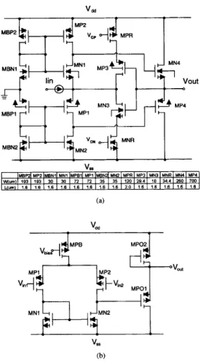
Fig. 6. (a) The 2-D structure of the proposed silicon retina where two decoders are used to decode the input address and then activate the control lines of the cells, two Rm amplifiers are used to convert the cell currents into the voltages, and the output buffer amplifies the voltage difference to obtain the output voltage. (b) The basic cell of the 2-D silicon retina where two control lines row and are generated from the row decoder, and four switches are used to control the current flow.
the cell. The row decoder decodes the m row address bits and activates one of 2" row control signals row and Tow. The column decoder decodes the n column address bits to activate one of 2n output channels in the multiplexer. Through the
multiplexer, the selected output channel sends out the inner and the outer emitter currents of the selected cell to the two tunable Rm amplifiers, and the input cell currents are converted into the voltages. Then, the two voltages are sent to the output differential amplifier with the gain A , . The output voltage V,,,
of the differential amplifier can be expressed as
where 1 g m n 3
+
gmp3 Rm Z A , - * ( l + 2gmp 1 Qmnl gdpl+
g d n lAs shown in Fig. 6(b), the basic cell contains a PNP pho- totransistor pair and four NMOS switches. In the chip layout, each cell has equal distance to its four nearest neighbors. The four switches in the cell are controlled by the row control signal row and its complement signal mw. When one row of the silicon retina cells is selected by the row address bits, the control signal row of this row is activated to high, whereas,
Tow is low. Thus, SW1 and SW2 are closed to connect the two
I I I L
1 1
vss
(b)
Fig. 7. The circuit diagrams of (a) the CMOS wideband Rm amplifier and (b) the CMOS output buffer used in the silicon retina chip.
emitters to the multiplexer. Through the multiplexer, they are further connected to the inputs of the Rm amplifiers, which are kept at virtual ground. Thus, the emitters are nearly grounded to send out le,outer and Ie,inner. At the same time, SW3 and SW4 are open to prevent the emitter currents from flowing into the ground. Oppositely, when the row of the silicon retina cells isn't selected, the control signal row of this row is low, and
Tow is high. Then, SW1 and SW2 are open to prevent the emitter currents from reaching the multiplexer and the output amplifier. Meanwhile, SW3 and SW4 are closed to connect both emitters to ground so that the deselected emitter currents are bypassed to ground.
The circuit diagrams of the Rm amplifier and the output buffer are shown in Fig. 7(a) and (b), respectively. The Rm amplifier in Fig. 7(a) with the shunt-shunt feedback config- uration offers a very low input impedance, a good linearity, and a high frequency bandwidth [14]. In Fig. 7(a), the basic
I-V conversion is achieved by the common-gate transistor
MNl(MP1) and the current source device MP2(MN2). The transistors MN4 and MP4 form a source-follower output buffer to enhance the driving capability and decrease the output impedance. The transistors MN3 and MP3, which offer a
894 IEEE JOURNAL OF SOLID-STATE CIRCUITS, VOL. 30, NO. 8, AUGUST 1995
~
Cont~ol Voltage (Vx-Vcp)
Transresistance (r,,,) Input Impedance (ri,) Output Impedance (ro) -3dB Frequency (f-fdb) +2.5V
-
-0.9V 919 Ohm-
1914 Ohm 44.6 Ohm-
88.2 Ohm 2.34 Ohm - 44.6 Ohm 246.3 MHz-
97.4 MHz TABLE ITHE EXPERIMENTAL RESULTS OF THE FABRICATED RM AMPLIFIER
feedback path from the output stage, are used to reduce both input and output impedances. The transistors MNR and MPR are used to adjust the gain of the Rm amplifier. The output buffer in Fig. 7(b) consists of a basic differential amplifier and a source-follower. The differential amplifier produces an output voltage that is proportional with l e , i n n e r -
le,outer
whereas, the source-follower offers a large driving capability to drive the output pads. The typical measured characteristics of the fabricated Rm amplifier are listed in Table I.
In the structure of Fig. 6(a), the output signal of each cell can be accessed by sending a set of address bits. The whole image frame can be obtained pixel-by-pixel by sending a sequence of address bits. If parallel outputs are preferred, the column decoder and the multiplexer can be omitted, and the
n outputs can be obtained through n-output amplifiers. In this way, the whole image frame can be obtained row-by-row by sending a sequence of row address bits.
In this paper, two experimental 32
*
32 silicon retina array chips have been designed and fabricated by using 0.8 pm double-poly double-metal N-well CMOS process. One of the chips is designed with both Rm amplifier and output buffer as shown in Fig. 6(a) to measure the full function of the silicon retina. The other is designed without Rm amplifiers and output buffer to measure the cell current directly. Both cell arrays have a fill factor of 0.33.In the proposed silicon retina, there are four NMOS switches, two phototransistors, and five interconnection lines as shown in Fig. 6(b). Generally, the NMOS switches are noncritical devices, and the minimum device dimension can be used. The phototransistor area can be reduced to the limit where the generated minimum photocurrent can be detected. The two major limitations on cell compaction are 1) the layout design rules, especially those for the N-well spacings and 2) the number of available interconnection levels to route the five cell signal lines compactly. In this experimental work, the cell is designed by using a relaxed design rule, and the cell area is 60 pm
*
60 pm. Further cell area reduction can be done by pushing the cell layout to the minimum design rules. To measure the performance of the new silicon retina cell array, a low-power He-Ne laser and several lens are used to generate a definite input image for test. Because of the serious scattering of the regular light source [ 131, it cannot be used to generate the input image. However, since the retina is made of semiconductor silicon, it will function well under regular light. In the test setup, the lens focus the low-power laser beam to a small light spot that is incident upon the silicon retina cells. In the measurement of the smooth characteristic of the outer phototransistor array, the laser light spot is incident upon the comer of the silicon retina array. Fig. 9(a) shows(b) Fig. 8.
photograph of the 2-D silicon retina.
(a) The chip photograph of the 2-D silicon retina and (b) the cell
the measured l e , i n n e r of the inner phototransistor array in the
2-D plot, whereas, Fig. 9(b) shows the measured le,outer of
the outer phototransistor array in the 2-D plot. As discussed above, le,inner represents the local intensity of the input image, whereas, le,outer represents the smoothed input image. Comparing Fig. 9(a) with (b), it can be seen that the outer phototransistor array really smoothes the whole input image. To see the detail, the contents on the line y = 5 in Fig. 9(a)
and (b) are selected to display in Fig. 10 where the measured le,inner is scaled down by a factor of 0.25 for easy comparison with Ie+ter. Since the light spot has some diffraction effects,
WU AND CHIU: A NEW STRUCTURE OF THE 2-D SILICON RETINA
The Measured le,inner
Y-axis
The Measured le,outer
S.OE-O&
Y-axis
(b)
Fig. 9. (a) The measured emitter current l e , i n n e r of the inner PNP photo- transistors plotted in the 2-D diagram and @) the measured emitter current
le,outer of the outer phototransistor array in the silicon retina chip.
7.0E-06 6.OE-06
[h
le,outer-
The measured P LoE4S-
The simulated3.oE-06
-
The simulated20E-06 currant source
1.0E-06 O.OE+OO
1
LOE*6
m 2 T ; N F x-axisFig. 10. The curves of y = 5 in Fig. 9(a) and (b) for the measured l e , i n n e r and the measured le,outer. respectively. The corresponding le,outer from simulation is also plotted together for comparison.
its effective incident area covers twelve pixels of cells so that l e , i n n e r in these cells is not zero as may be seen in Fig. 10. Comparing the curves of le,inner and
le,outer,
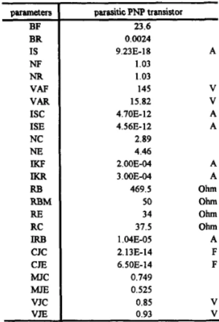
the smooth effect of the outer phototransistor array can be verified.To analyze the function of the outer phototransistor array using the proposed equivalent circuit in Fig. 3, the device parameters of the PNP bipolar transistors are measured first. Table
II
shows the measured device parameters of the PNP transistor. Ideally, both inner and outer phototransistors have the same photogeneration current. Thus, the emitter currentl e , j n n e r of the inner phototransistor is used as the input current
of the light-incident outer phototransistors in the simulation.
Fig. 11 shows the 2-D graph for the SPICE simulated
le,outer
895
The Simulated ie,outer
28
Y-axis
Fig. 11. The simulated emitter current le,outer of the 2-D silicon retina.
TABLE 11
THE DEVICE P A R A M E T E R S OF THE PARASITIC PNP
TRANSISTOR IN 0.8 p~ DPDM CMOS PROCESS P -BF BR IS NF NR VAF VAR ISC ISE NC NE K F IKR RB RBM RE RC IRB CJC CJE MJC MJE VJC VJE ~~ parasitic PNP transistor 23.6 0.0024 9.23E-I8 1.03 1.03 145 V 15.82 V 4.7OE-12 A 4.56E-12 A A 2.89 4.46 2.00E-04 A 3.00E-04 A 469.5 Ohm 50 O h 34 O h 37.5 O h 1.04E-05 A 2.13E-14 F 6.5OE-14 F 0.749 0.525 0.85 V
of the outer phototransistor array with
RN
in Fig. 3 equalto 2.8 kR. To further investigate the measured data and the simulated data, the contents on the line y = 5 in Fig. 11 for the simulated
le,outer
are also plotted in Fig. 10 for comparison. The consistence between the simulatedle,outer
curve and the measuredle,outer
is good, which proves the suitability of the proposed equivalent circuit in Fig. 3 in simulating the behaviorof the outer phototransistor array as the smooth network. In Fig. 10, the simulated le,outer curve is slightly sharper
than the measured The deviation near the comer may
be caused by the edge effect of the smoothing array. On the other hand, the deviations for x
>
3 could be causedby the surface recombination effect mentioned in Section 11, which is not considered in the equivalent circuit of Fig. 3.
Due to the surface recombination effect, the measured le,outer
is smaller in those dark cells close to the light-incident cells. The surface recombination effect can be characterized by connecting suitable current sources between the base of the
896
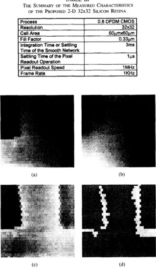
Process Resolution
Cell Area
IEEE JOURNAL OF SOLID-STATE CIRCUITS, VOL. 30, NO. 8, AUGUST 1995
0.8 DPDM CMOS 32x32 60ur 4.OE-01 O.OE+OO
k
-4.OE-01-
B -8.OE-01 Readout Operation Pixel Readout Speed Frame Rate 1 .OE+OO 8.OE-01 g 4.OE-01 1 MHz 1 KHz 2.OE-01 O.OE+OO -2.OE-01 -4.OE-01 X-axis (b)Fig. 12. (a) The measured output voltages of the 2-D silicon retina with a large light spot incident upon it, which are plotted in the 2-D diagram to show the edge detection characteristics. (b) The curves of y = 8 in (a) are plotted to observe the edge detection capability clearly.
phototransistors and the ground. The use of these current
sources decreases so that it is more consistent with
the measured values as shown in Fig. 10.
To measure the edge-detection effect of the proposed silicon retina, the laser light spot is incident upon the chip. Fig. 12(a) shows the 2-D plot of the measured output voltages
Vout
of each cell through the on-chip Rm amplifier and output buffer. As shown in Fig. 12(a), a voltage change from positive to negative is obtained around the edge of the incident light spot. To observe the response clearly, the curves of y = 8 is shown in Fig. 12(b). In the Fig. 12(b), a voltage change from positive to negative around the edge of the spot located at the vicinity of z = 6, can be seen clearly. By detecting the change, the edge-detection of the proposed silicon retina can be performed in the image processing system.According to the measurement, the smooth network of the experimental chip takes about 3 ms to settle down. In reading out the pixel signal, it takes about 1 ps to settle down the de- code switch introduced transients. Thus, the maximum readout operation frequency is about 1 MHz, and the equivalent frame rate is about 1 kHz. The measured results of the fabricated CMOS retina chip are summerized in Table 111. Generally, the scaled down cells could decrease the settling times in both smooth network and readout operation. Thus, the maximum operational frequency and the frame rate could be improved.
To further evaluate the performance of the proposed sil- icon retina, a simple image is used as the input to the fabricated retina, and the output characteristics are measured. Fig. 13(a)-(c) shows the inner image, the outer image, and the difference image, respectively, when a character
“T”
patternTABLE 111
THE SUMMARY OF THE MEASURED CHARACTERISTICS
OF THE PROPOSED 2-D 32x32 SILICON RETINA
_ - ~
Fill Factor
lntwration Time or Settling I
-23
0.33 m Time of the Smooth NetwokI
Settling Time of the Pixel
I
1 CISFig. 13. The measured output images when a character image “T” is incident on the chip. (a) The output image of the inner array, (b) the output image of
the outer array, (c) the output image of the retina chip, (d) the output image of (c) with only positive pulses only.
is incident upon the silicon retina. In this test pattern, the light intensity decreases gradually from the left-up to right- bottom as showed in Fig. 13(a). Under such nonuniform light intensity, the silicon retina still functions well in this measurement. In Fig. 13(c), the edge of the pattern ‘‘7”’ stands
out from the bright light. In Fig. 13(d), only the positive pulses of the response in Fig. 13(c) are chosen, and the resulting image becomes more clear. From the above results, it has been verified that the proposed silicon retina can perform the function of edge-detection.
The most important characteristic of the retina is to detect a moving image. As discussed in Section 11, the moving target detection can be performed by applying a moving image passing across the silicon retina. Fig. 14 shows the measured output voltages of the cell (24, 18) and the cell (24, 26). At the moment when the front edge of the moving pattern passes across the measured cells, two successive positive voltage pulses, which are proportional to l e , i n n e r - le,outer
WU AND CHIU: A NEW STRUCTURE OF THE 2-D SILICON RETINA 897
REFERENCES
Fig. 14.
cells with a moving pattem passing across the chip.
The measured response of VoUt in two of the 2-D silicon retina
can be recorded on the scope trace as shown in Fig. 14. Similarly, two negative voltage pulses, which are proportional
to Ie,inner - can be obtained when the back edge of
the moving pattern leaves the measured cells. By detecting the pulses, the moving object can be detected. At the same time, some information about the moving object can also be obtained from the characteristics of the output voltage pulses.
IV. CONCLUSION
A new structure of the silicon retina cell that contains only two isolated PNP phototransistors is proposed and analyzed. In this structure, the smooth network is implemented by the phototransistors in a common open-base region. Experimental results verify the retinal functions of both edge detection and moving image detection. The new structure has very simple interconnection and wiring. The layout is compact, and the resultant chip area is small. Thus, it is feasible to realize the new silicon retina with the associated image processing neural network in VLSI. Further research on this new structure will focus on device characterizations and applications.
ACKNOWLEDGMENT
The authors would like to acknowledge the suggestions and comments of the reviewers which led to the substantial improvements in this paper, and the Chip Implementation Center (CIC) of National Science Council (NSC) of Taiwan, R . O . C . for their support in chip fabrication.
[ 11 P. A. Ruetz and R. W. Brodersen, “Architectures and design techniques for real time image processing ICs,” IEEE J. Solid-state Circuits, vol.
SC-22, pp. 233-250, Apr. 1987.
[2] M. Maruyama, H. Nakahira, T. Araki, S. Sakiyama, Y. Kitao, K. Aono, and H. Yamada, “An image signal multiprocessor on a single chip,”
IEEE J . Solid-state Circuits, vol. 25, pp. 1476-1483, Apr. 1990.
[3] J. Dowling, The Retina: An Approachable Part of the Brain. Cam- bridge, MA: Harvard University Press, 1987.
[4] D. Marr, Vision.
[SI C. A. Mead, Analog VLSI and Neural Systems. Reading, MA: Addison Wesley, 1989.
[6] C. A. Mead and M. A. Mahowald, “A silicon model of early visual processing,” Neural Networks, vol. 1, pp. 91-97, 1988.
[7] H. Kobayashi, J. L. White, and A. A. Abidi, “An active resistor network for Gaussian filtering of images,’’ IEEE J. Solid-state Circuits, vol. 26,
pp. 738-748, May 1991.
[8] P. C. Yu, S. J. Decker, H. S. Lee, C. G. Sodini, and J. L. Wyatt, “CMOS resistive fuses for image smoothing and segmentation,” IEEE
J. Solid-state Circuits, vol. 27, pp. 545-553, Apr. 1992.
[9] C. P. Chong, C. Andre, T. Salama, and K. C. Smith, “Image-motion detection using analog VLSI,” ZEEE J. Solid-state Circuits, vol. 27, pp.
93-96, Jan. 1992.
[lo] A. Moini, A. Bouzerdoum, A. Yakovleff, D. Abbott, 0. Kim, K. Eshraghian, and R. E. Bogner, “An analog implementation of early visual processing in insects,” in 1993 VLSlTSA, pp. 283-287.
[ 1 13 T. Delbruck, “Silicon retina with correlation-based, velocity-tuned pix- els,” IEEE Trans. Neural Networks., vol. 4, pp. 529-541, May 1993. [12] T. I. Kamins and G. T. Fong, “Photosensing arrays with improved spatial
resolution,” IEEE J. Solid-state Circuits, vol. SC-13, pp. 8G85, Apr.
1978.
[13] C. Y. Wu and C. F. Chiu, “A new structure for the silicon retina,” in
IEDM Tech. Dig., Dec. 1992, pp. 4 3 9 4 2 .
[14] P. H. Lu, C. Y. Wu, and M. K. Tsai, “VHF bandpass filter design using CMOS transresistance amplifiers,” in Proc. IEEE Int. Symp. Circuits
Syst., May 1993, pp. 99G993.
San Francisco, CA: W. H. Freeman, 1982.
Chung-Yu Wu (S’76-M’76) received the M.S and Ph.D. degrees from the Department of Electronics Engineering, National Chiao-Tung University, Tai- wan in 1976 and 1980, respectively.
From 1980 to 1984, he was an Associate Pro- fessor with the National Chiao-Tung University. During 1984-1986, he was a Visiting Associate Professor with the Department of Electncal Engi- neering, Portland State University, Oregon. Since 1987, he has been a Professor with the National Chiao-Tung University. He has published more than 50 journal papers and 60 conference papers on several topics, including digital integrated circuits, analog integrated circuits, computer-aided design, ESD protection circuits, special semiconductor devices, and process technologies. He also has eight patents including four US patents. His current research interests focus on low-voltage mixed-mode integrated circuit design, hardware implementation of visual and auditory neural systems, and RF integrated circuit design.
Dr Wu is a member of Eta Kappa Nu and Phi Tau Phi.
Chin-Fong Chiu (S’92-M’95) was born in Taipei,
Taiwan, Republic of China, in 1966. He received the B.S. degree from the Department of Electron-
ics Engineering, National Chiao-Tung University, Hsinchu, Taiwan, in 1988. He is currently working toward the Ph.D. degree at the same institute.
His main research interests have been in neural networks, pattern recognition, and analog integrated circuits and systems.