3852 Journal of The Electrochemical Society, 146 (10) 3852-3855 (1999) S0013-4651(99)03-017-7 CCC: $7.00 © The Electrochemical Society, Inc.
A p1-poly-Si gate has been proposed for the fabrication of sur-face-channel p-metal oxide semiconductor field effect transistors (p-MOSFETs) in deep submicrometer complementary MOS (CMOS).1 Surface-channel devices exhibit a better threshold, subthreshold leakage control, and short channel effect control than those of the conventional buried-channel using the n1-poly-Si gate for p-MOS-FETs. However, boron, coming from the BF12- implantation, pene-trates easily from poly-Si gate through the gate oxide during the fol-lowing high temperature thermal cycles at the presence of F.2To suppress the boron penetration, methods, such as the stacked poly-Si gate,3 nitrided oxide,4 oxide gettering,5 and nitrogen coimplanta-tion6have been reported. However, there is little report on the re-placement of implantation source (BF12) by the solid diffusion source. The Si-B film that deposited in the ultrahigh vacuum chem-ical vapor deposition (UHV/CVD) system has been reported as the polycrystalline structure with extraordinary high B concentration (23 1022/cm3).7Hence, Si-B can be used as a solid diffusion source to form the p1/n diode due to its high B concentration, and the smaller surface concentration and diffusivity.8These shallow junc-tions formed by the Si-B solid diffusion source exhibited better char-acteristics than those of conventional BF12-implanted junctions in terms of uniformity, ideality factor, and reverse current. In this paper, a novel Si-B layer, for the first time, is proposed as the solid diffu-sion source for doping the poly-Si as the p1-poly-Si for
p-MOS-FETs to alleviate the boron penetration problem. It is found that this new process, which is free of F, depicts a better capability of sup-pressing the boron penetration than conventional methods employ-ing BF21, or B1implantation.
Experimental
p1-Poly-Si gate MOS capacitors were fabricated on n-type Si(100) wafer with resistivity of 2-4 V cm. Field oxide, 550 nm, was grown and active areas were defined. A thin gate oxide 9.5 nm was grown at 9008C. A 300 nm poly-Si was then deposited. Samples with the conventional p1-poly-Si gate were conducted by implanting BF21, 50 keV, to a dose of 5 3 1015cm22; or B1, 20 keV, to a dose of 5 3 1015cm22. While for the Si-B sample, they were put into a UHV/CVD system to deposit a 35 nm Si-B layer using a 1:1 mixture of the pure SiH4and B2H6(1% in H2) at 5508C. The base pressure was 2 3 1028Torr. Afterward, all samples were annealed in a wet O2ambient at the temperature between 850 and 9508C for 15-35 min. Si-B layer was oxidized in this annealing process to form SiO2 and the B diffused into the underlying poly-Si gate forming the p1 -poly-Si gate. The formed oxides were then dipped away. Al metal was deposited and patterned for contacts. After aluminum metalliza-tion, all samples were annealed at 400°C for 30 min in an N2 ambi-ent to form a good ohmic contact. The comprehensive effects on the annealing temperature (875-950°C) and time (15-35-min) on the p1
-A Novel Si-B Diffusion Source for p
1
-Poly-Si Gate
Tien Sheng Chao,
aChung Ping Kuo,
bT. P. Chen,
cand Tan Fu Lei
b aNational Nano Device Laboratories, Hsinchu 300, TaiwanbDepartment of Electronics Engineering and Institute of Electronics, National Chiao Tung University, Hsinchu, Taiwan cUnited Micro Electronics Corporation, Science-Based Industrial Park, Hsinchu, Taiwan
In this paper, we report a novel Si-B diffusion source for p1-poly-Si gate p-metal oxide-semiconductor field effect transistors (p-MOSFETs). It is found that boron penetration can be effectively suppressed using this process. All the electrical properties of the MOS capacitors are significantly improved over the conventional BF12or B1-implanted samples. This process is very promising for fabrication of future surface-channel p-MOSFETs.
© 1999 The Electrochemical Society. S0013-4651(99)03-017-7. All rights reserved. Manuscript submitted March 1, 1999; revised manuscript received June 2, 1999.
Figure 1. High frequency C-V curves of the Si-B outdiffused, B-implanted,
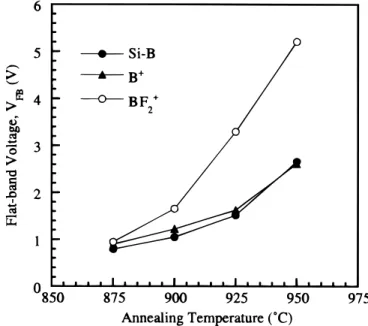
and BF12-implanted gate capacitors annealed at 900°C for 15 min. Figure 2. The flatband voltage as a function of the annealing temperatures.
) unless CC License in place (see abstract).
ecsdl.org/site/terms_use
address. Redistribution subject to ECS terms of use (see
140.113.38.11
Journal of The Electrochemical Society, 146 (10) 3852-3855 (1999) 3853 S0013-4651(99)03-017-7 CCC: $7.00 © The Electrochemical Society, Inc.
poly-Si MOS capacitors using Si-B layer are compared with the con-ventional BF12- and B1-ion-implanted counterparts using secondary ion mass spectroscopy (SIMS) analyses, high/low frequency capac-itance voltage (C-V) measurement, current density vs. electric field (J-E) characteristics, charge-to-breakdown (Qbd), and breakdown field (Ebd).
Results and Discussion
The flatband voltage shift, VFB, is frequently used to indicate the
boron penetration effect in the p1-poly-Si gate MOS capacitors. Basically, the more increases of VFBto positive indicates the more
boron penetration. The normalized high frequency (1 MHz) C-V curves Ch/Cox for capacitors with the Si-B, B1, and BF12-implanted gates, annealed at 9008C for 15 min, are shown in Fig. 1. The Si-B sample exhibits the smallest positive flatband and threshold voltage shifts compared to those of BF12 and B1 samples, while the BF21 sample has the largest shift due to the boron penetration enhanced by F. The B1sample is in between. This implies that Si-B sample has a better retardation of B penetration than BF21or B1. The flatband
voltage as a function of the annealing temperature at 850-9508C for 15 min is shown in Fig. 2. Basically, the flatband voltage increases as the annealing temperature increases. The flatband voltage shift is the smallest for the Si-B sample among these three samples in the whole range of annealing temperature, while BF12 sample exhibits the largest values among all annealing temperatures. The shift of the B1 sample is found in between. The Ch/Cox shows the same trend (not shown) as the annealing time is increased to 35 min for these sam-ples. It is found that the Si-B sample is still the smallest one among these three samples and shows little shifting of flatband voltage.
Quasi-static Cq/Cox curves are shown in Fig. 3a and b for Si-B and BF21samples. The Cq/Cox curves of the BF12 samples exhibit the shift and distortion as the annealing temperatures exceeds 900°C, while Cq/Cox of the Si-B sample is shown to be stable at tempera-tures up to 9258C. This implies that the Si-B sample has a better ther-mal stability than that of the BF12 samples.
Figure 3. The quasi-static C-V characteristics of the (a) Si-B outdiffused, (b)
BF21-implanted gate capacitors at different annealing temperatures.
Figure 4. The J-E characteristics of the Si-B outdiffused, B-implanted, and
BF12-implanted samples annealed at 9258C for 15 min.
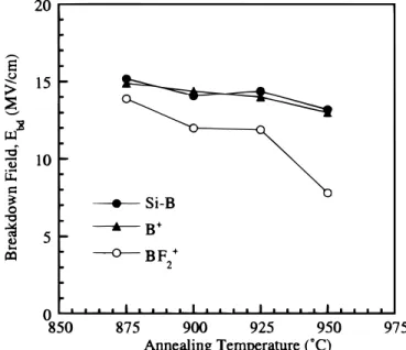
Figure 5. The dielectric breakdown field at different temperatures for Si-B
outdiffused, B-implanted, and BF21-implanted samples.
) unless CC License in place (see abstract).
ecsdl.org/site/terms_use
address. Redistribution subject to ECS terms of use (see
140.113.38.11
3854 Journal of The Electrochemical Society, 146 (10) 3852-3855 (1999) S0013-4651(99)03-017-7 CCC: $7.00 © The Electrochemical Society, Inc. J-E characteristics of the samples after annealing at 9258C for
15 min are plotted in Fig. 4. The BF21sample shows an early Fowler-Nordheim (F-N) tunneling at the low field and a smaller electric breakdown field, Ebd. Ebdof the B1sample is almost the same as the Si-B. In Fig. 5, the average of Ebdof the three samples is compiled. Basically, the higher the annealing temperature, the lower the Ebd. Further, the Ebd of the BF21 sample decreases more rapidly with increasing annealing temperature than the Si-B sample.
The Weibull plots of the charge-to-breakdown for BF12 and Si-B are plotted and shown in Fig. 6a and b. The stressing current densi-ty is 100 mA/cm2. The gate area is 4.42 3 1025cm2. While the Qbd decreases slightly as the annealing temperature increases from 875 to 950°C for the Si-B sample (Fig. 6a), the Qbddegrades (lower and wider) significantly for BF21sample as the annealing temperature increases from 9008C (Fig. 6b). The average Qbdfor these three ples annealed at 875 to 950°C are compiled in Fig. 7. The Si-B
sam-ple exhibits the largest Qbdthan those of B1and BF12 samples in all temperature ranges. The B1sample value is between those of Si-B and BF12.
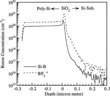
Figure 8 shows the boron profiles of the Si-B and BF21 -implant-ed samples anneal-implant-ed at 925°C for 15 min by using SIMS analyses. Si-B sample shows a smaller concentration at both the SiO2and the Si substrate, while maintaining a higher B concentration in the poly-Si film. This reduces the gate resistivity and has the advantage in the high frequency applications.
From the above result, it can be found that the Si-B layer deposit-ed on the poly-Si gate as the diffusion source for p1-poly-Si is the best one among these three samples. The reasons for these improve-ments can be as follows. (i) Outdiffusion from the Si-B layer does not introduce F inside the poly-Si using Si-B layer. F has been iden-tified as the key factor to enhance B diffusion. (ii) It is a solid phase diffusion source. The dopant, boron, from Si-B film is deposited instead of implanted. Hence, no defects are induced by use of this
Figure 6. The Weibull plots of charge-to-breakdown for (a) Si-B, and (b)
BF21samples annealed at different temperatures.
Figure 7. The charge-to-breakdown at different temperatures for Si-B
out-diffused, B-implanted, and BF12samples.
Figure 8. SIMS boron profiles in poly-Si/SiO2/Si for Si-B outdiffused and
BF12-implanted samples annealed at 9258C for 15 min.
) unless CC License in place (see abstract).
ecsdl.org/site/terms_use
address. Redistribution subject to ECS terms of use (see
140.113.38.11
Journal of The Electrochemical Society, 146 (10) 3852-3855 (1999) 3855 S0013-4651(99)03-017-7 CCC: $7.00 © The Electrochemical Society, Inc.
process. In addition, the boron diffuses from the surface of poly-Si for Si-B sample instead of starting to diffusing from halfway in poly-Si for the BF21- or B1-implanted sample. Hence, the Si-B sample has a longer diffusion path to the poly-Si/oxide interface than that of BF21or B1sample.
Conclusion
A novel Si-B diffusion source for p1-poly-Si gate in p-MOSFETs has been investigated for the first time in this study. This process shows the best performance for suppressing the boron penetration over the conventional BF12 or B1-implanted samples in a wide range of annealing temperatures and times. This process is a very promising candidate for fabricating the surface-channel p-MOSFETs in deep submicrometer CMOS.
National Nano Device Laboratories assisted in meeting the publication costs of this article.
References
1. G. J. Hu and R. H. Bruce, IEEE Trans. Electron Devices, ED-32, 584 (1985). 2. H. H. Tseng, M. Orlowski, P. J. Tobin, and R. L. Hance, IEEE Electron. Device Lett.,
13, 14 (1992).
3. S. L. Wu, C. L. Lee, and T. F. Lei, Tech. Dig. Int. Electron Devices Meet., 329 (1993). 4. L. K. Han, D. Wristers, J. Yan, M. Bhat, and D. L. Kwong, IEEE Electron Device
Lett., 16, 319 (1995).
5. T. H. Lin, C. L. Lee, T. S. Lei, and T. S. Chao, IEEE Electron Device Lett., 16, 164 (1995).
6. T. S. Chao, M. C. Liaw, C. H. Chu, C. Y. Chang, C. H. Chien, C. P. Hao, and T. F. Lei, Appl. Phys. Lett., 69, 1781 (1996).
7. T. P. Chen, T. F. Lei, H. C. Lin, C. Y. Chang, W. Y. Hsieh, and L. J. Chen, Appl. Phys. Lett., 64, 1853 (1994).
8. T. F. Lei, T. P. Chen, H. C. Lin, and C. Y. Chang, IEEE Trans. Electron Devices, 42, 2104 (1995).
) unless CC License in place (see abstract).
ecsdl.org/site/terms_use
address. Redistribution subject to ECS terms of use (see
140.113.38.11