IEEE ELECTRON DEVICE LETTERS, VOL. 24, NO. 3, MARCH 2003 153
Wide Range Work Function Modulation of Binary
Alloys for MOSFET Application
Bing-Yue Tsui, Senior Member, IEEE, and Chih-Feng Huang, Student Member, IEEE
Abstract—This paper explores the characteristics of the binary alloys Ta–Pt and Ta–Ti for gate electrode application. With a proper composition of high and low work function metals, the work function of the metal alloys can be modulated from 4.16 eV to 5.05 eV continuously. The alloys show good thermal stability and inner chemical activity on both silicon dioxide and hafnium dioxide. Thermal stress generated from the alloy film increases interface state density and hence effective oxide charges. This problem can be greatly reduced with W/Ta–Pt stack structure, where W acts as the main conducting metal and Ta–Pt acts as work function control metal. All of these properties make them suitable for use in all device applications.
Index Terms—Alloy, metal gate, work function.
I. INTRODUCTION
A
S MOS devices are scaled down, the gate oxide thick-ness will decrease to be thinner than 2 nm. Several prob-lems were observed together with the thin down of gate oxide such as poly-Si gate depletion, boron penetration, quantum ef-fect, and gate leakage current [1]–[4]. Using metal to replace poly-Si as gate electrode can solve the first two problems [5], [6]. However, to fabricate surface channel devices with suitable threshold voltage , the gate electrode should have suitable work function ( , i.e., metals with –4.2 eV and –5.2 eV are suitable for NMOSFETs and PMOS-FETs, respectively. It was reported that the of metal nitrides could be modulated with the nitrogen content [7]–[9]. Unfortu-nately, the magnitude of modulation is not wide enough. Re-cently, metal alloys were proposed for work function modula-tion [10], [11]. However, the drops abruptly once new alloy phase forms. Ni–Ti inter-diffusion was also proposed to produce dual work function metal gate [12], but the thermal stability is poor.In this work, we propose a new Ta-based binary alloy system of Ta–Pt and Ta–Ti. Wide range and continuous modulation from 4.16 eV to 5.05 eV could be achieved.
II. EXPERIMENTS
A simple MOS structure was fabricated to characterize the binary alloy systems. The starting material was (100)-oriented phosphorus doped Si wafer. Following standard RCA cleaning,
Manuscript received October 29, 2002; revised January 2, 2003. This work is supported by the National Science Council of Taiwan, R.O.C., under Con-tract NSC-90-2215-E-009-064. The review of this letter was arranged by Editor T.-J. King
The authors are with the Department of Electronics Engineering and the In-stitute of Electronics, National Chiao Tung University, Hsinchu 300, Taiwan, R.O.C. (e-mail: bytsui@cc.nctu.edu.tw).
Digital Object Identifier 10.1109/LED.2003.809528
gate oxide of 11-nm-thick was thermally grown. The gate electrodes were patterned using the liftoff process. Ta Pt and Ta Ti alloys were cosputtered to a thickness of 60 nm on patterned photoresist. Table I lists the deposition conditions and the atomic composition analyzed with Rutherford Backscat-tering Spectroscopy (RBS). After gate patterning, samples were annealed in N ambient at 400, 500, and 600 C for 30 min followed by Al deposition at the back.
III. RESULTS ANDDISCUSSION
The work function of an A B alloy can be approximately expressed as
where and are the pure constituent work functions of A and B, respectively, and and are the pure constituent total densities of states [14]. The density of states at Fermi en-ergy is proportional to the electronic specific heat
con-stant , where is Boltzmen constant
and is temperature. In the case of , the
changes with linearly as [15]. The
values of Pt, Ta, and Ti are 6.8, 5.9, and 3.35 mJ/mole/K , re-spectively [16]. Since the values of Ta and Pt are very close, a nearly linear correlation can be expected.
The approximate work function ( of annealed samples was extracted by comparing the measured capaci-tance–voltage ( – ) curves with the theoretical – curve
[9], [13]. The is defined as – ,
where is effective oxide charges and is capacitance at accumulation mode. As the gate oxide thickness is 11 nm, a of 1 10 cm results in a deviation of 0.05eV only. Fig. 1 shows the extracted of 400 C annealed samples. The of poly-Si gate devices is around 5 10 cm . The of metal gate devices might be higher than that of poly-Si gate. However, since the interface state density ( ) of metal gate devices is similar to that of poly-Si gate, it is believed that the of metal gate will not be much higher than that of poly-Si gate. Therefore, the should be very close to the . With increasing contents of high elements, Pt in Ta–Pt alloys or Ta in Ta–Ti alloy, the shifts toward higher value. The Ta Ti alloy and Ta Pt alloy
154 IEEE ELECTRON DEVICE LETTERS, VOL. 24, NO. 3, MARCH 2003
TABLE I
DEPOSITIONCONDITIONSUSED INTHISWORK ANDATOMICCOMPOSITIONS OFALLOYSANALYZEDWITHRBS
Fig. 1. Extracted approximate work function(8 ) of 400 C annealed samples.
show of about 4.16 eV and 5.05 eV and is suitable for NMOSFETs and PMOSFETs, respectively. As expected, the can be modulated continuously by adjusting the atomic composition of the alloy. This property allows for the use of the alloy system to obtain precise work function. For example, fully-depleted SOI devices require of close to 4.6 eV [17], and can be achieved using the alloys with Ta/Pt ratio close to 0.74/0.26.
Fig. 2(a) and (b) show the Transmission Electron Mi-croscopic (TEM) micrographs of Ta Pt /SiO and Ta Ti /SiO structures after annealing at 600 C, respec-tively. The alloys are almost amorphous and no interfacial layer was formed. Furthermore, no compound phases were observed from the X-ray diffraction (XRD) spectrums. The change of EOT after annealing at 600 C is less than 1%, i.e., less than 0.1 nm. These results imply that the alloys are thermally stable up to 600 C on SiO . This temperature is high enough for replacement gate process and is better than most of low work function elemental metals such as Ti [18].
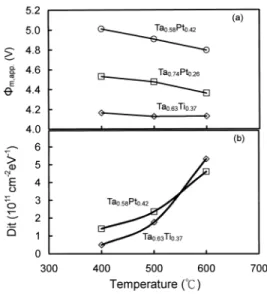
Fig. 3(a) shows that the decreases slightly with the increase of annealing temperature. Since the alloys are ther-mally stable on SiO , this phenomenon cannot be attributed to the interaction between alloy and oxide. Fig. 3(b) shows that the also increases with the increase of annealing temperature. It is thus postulated that the decrease of comes from the thermal stress generated oxide charges. To reduce the effect of thermal stress, a stack gate electrode of W(50 nm)/Ta–Pt(10 nm) is proposed. The thermal expansion coefficient of W (4.4
Fig. 2. Cross-sectional TEM micrographs of (a) Ta Pt /SiO structure and (b) Ta Ti /SiO structure after annealing in N ambient for 30 minutes at 600 C. No Interfacial reaction are observed.
Fig. 3. (a) Approximate work function (8 ) and (b) interface state density(D ) versus annealing temperatures.
10 C is lower than that of Pt (9.0 10 C and Ta (6.6 10 C and is close to that of Si (2.4 10 C . Another benefit of using stack structure is that the resistivity of W (5.3 10 -cm) is much lower than the resistivity of al-loys ( 300 10 -cm). In this structure, the Ta–Pt alloy de-termines the work function and the W layer serves as the main conducting material.
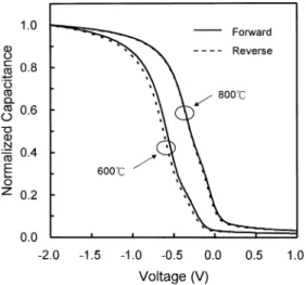
Fig. 4 shows the – characteristics of W(50 nm)/Ta–Pt(10 nm)/HfO (5 nm)/p-type Si structure after annealing at 600 C and 800 C in N ambient for 30 min. The apparent kink in the curve of 600 C annealed sample points to the insufficient
TSUI AND HUANG: WIDE RANGE WORK FUNCTION MODULATION 155
Fig. 4. C–V characteristic of the Ta Pt /HfO /p-Si sample after annealing at 600 C and 800 C in N ambient for 30 minutes.
passivation of interface states at the HfO /Si interface. The smaller kink and negligible hysteresis phenomenon of the 800 C annealed sample imply that the stack structure is stable up to 800 C. The reduction of kink and hysteresis also confirms that thermal stress can be reduced by the stacked metal gate. The flatband voltage difference between 600 and 800 C annealed devices may be attributed to the reduction of and/or the change of due to interaction between W and Ta–Pt or between Ta–Pt and HfO . A 900 C annealing distorts the – characteristic. The stability of metal gate/high-K dielectric system is under investigation.
IV. CONCLUSION
This work explores the characteristics of the binary alloys Ta–Pt and Ta–Ti for gate electrode application. With a proper composition of high and low work function metals, the work function of the metal alloys can be modulated from 4.16 eV to 5.05 eV continuously. The resistivity of Pt–Ta alloy is high and thermal stress of thick Ta–Pt alloy may generate oxide charges. Therefore, stack structure with a low resistivity and low stress layer as main conducting layer and the proposed alloy layer as work function control layer, for example W/Ta–Pt, is preferred for actual application.
To implement metal gate into CMOS process is tough not only for alloy gates. Metal gates for NMOS and PMOS can be patterned separately [19]. Using metal ion implantation to form various alloys is another choice; it depends on the matu-rity of metal ion implantation technology. However, gate elec-trode with work function near mid-gap of Si should be used for
FD-SOI. The proposed alloy system shows the advantage of pre-cise work function control in this aspect.
REFERENCES
[1] C. Y. Wong, J. Y. C. Sun, Y. Taur, C. S. Oh, R. Angelucci, and B. Davari, “Doping of n and p polysilicon in a dual-gate process,” in IEDM Tech. Dig., 1988, pp. 238–241.
[2] J. R. Pfiester, F. K. Baker, T. C. Mele, H. H. Tseng, P. J. Tobin, J. D. Hayden, J. W. Miller, C. D. Gunderson, and L. C. Parrillo, “The effects of boron penetration on p polysilicon gates MOS devices,” IEEE Trans. Electron Devices, vol. 37, pp. 1842–1851, Aug. 1990.
[3] S. H. Lo, D. A. Buchanan, Y. Taur, and W. Wang, “Quantum-mechan-ical modeling of electron tunneling current from the inversion layer of ultra-thin-oxide nMOSFETs,” IEEE Electron Device Lett., vol. 18, pp. 209–211, May 1997.
[4] Y. Taur, D. Buchanan, W. Chen, D. J. Frank, K. I. Ismail, S.-H. Lo, G. A. Sai-Halasz, R. G. Viswanathan, H.-J. C. Wann, S. J. Wind, and H.-S. Wong, “CMOS scaling into the nanometer regime,” Proc. IEEE, vol. 85, pp. 486–504, Apr. 1997.
[5] Y. Taur, C. H. Wann, and D. J. Frank, “25nm CMOS design considera-tion,” in IEDM Tech. Dig., 1998, pp. 789–792.
[6] Q. Lu, Y. C. Yeo, P. Ranade, H. Takeuchi, T. J. King, C. Hu, S. C. Song, H. F. Luan, and D. L. Kwong, “Dual-metal gate technology for deep-sub-micron CMOS transistor,” in Proc. Symp. VLSI Technology, 2000, pp. 72–73.
[7] H. Wakabayashi, Y. Saito, K. Takeuchi, T. Mogami, and T. Kunio, “A dual-metal gate CMOS technology using nitrogen-concentra-tion-controlled TiN film,” IEEE Trans. Electron Devices, vol. 48, pp. 2363–2369, Oct. 2001.
[8] Y. S. Suh, G. Heuss, H. Zong, S. N. Hong, and V. Misra, “Electrical char-acteristics of TaSiN gate electrodes for dual gate Si-CMOS devices,” in Proc. IEEE Symp. VLSI Technology, 2001, pp. 47–48.
[9] R. Lin, Q. Lu, P. Ranade, T. J. King, and C. Hu, “An adjustable work function technology using Mo gate for CMOS devices,” IEEE Electron Device Lett., vol. 23, pp. 49–51, Jan. 2002.
[10] H. Zhong, S. N. Hong, Y. S. Suh, H. Lazar, G. Heuss, and V. Misra, “Properties of Ru–Ta alloys as gate electrodes for NMOS and PMOS silicon devices,” in IEDM Tech. Dig., 2001, pp. 432–435.
[11] D. G. Park, T. H. Cha, K. Y. Lim, H. J. Cho, T. K. Kim, S. A. Jang, Y. S. Suh, V. Misra, I. S. Yeo, J. S. Roh, J. W. Park, and H. K. Yoon, “Robust ternary metal gate electrodes for dual gate CMOS devices,” in IEDM Tech. Dig., 2001, pp. 616–619.
[12] I. Polishchuk, P. Ranade, T. J. King, and C. Hu, “Dual work function metal gate CMOS transistors by Ni–Ti interdiffusion,” IEEE Electron Device Lett., vol. 23, pp. 200–202, Apr. 2002.
[13] B. Y. Tsui and C. F. Huang, “Investigation of Cu/TaNx metal gate for metal-oxide-silicon devices,” J. Electrochem. Soc., Jan. 2003, to be pub-lished.
[14] C. D. Gelatt, Jr. and H. Ehrenreich, “Charge transfer in alloys: AgAu,” Phys. Rev. B, vol. 10, no. 2, pp. 398–415, 1974.
[15] R. Ishii, K. Matsumura, A. Sakai, and T. Sakata, “Work function of bi-nary alloys,” Appl. Surf. Sci., vol. 169–170, pp. 658–661, 2001. [16] C. Kittel, Introduction to Solid State Physics, 5th ed. New York: Wiley,
1976, p. 167.
[17] L. Chang, S. Tang, T. J. King, J. Bokor, and C. Hu, “Gate length scaling and threshold voltage control of double-gate MOSFETs,” in IEDM Tech. Dig., 2000, pp. 719–722.
[18] C. Y. Ting, M. Wittmer, S. S. Iyer, and S. B. Brodsky, “Interaction between Ti and SiO2,” J. Electrochem. Soc., vol. 131, no. 12, pp. 2934–2938, 1984.
[19] Y. C. Yeo, Q. Lu, P. Ranade, H. Takeuchi, K. J. Yang, I. Polishchuk, T. J. King, C. Hu, S. C. Song, H. F. Luan, and D. L. Kwong, “Dual-metal gate CMOS technology with ultrathin silicon nitride gate dielectric,” IEEE Electron Device Lett., vol. 22, pp. 227–229, May 2002.