行政院國家科學委員會補助專題研究計畫期中報告
ㄧ個全新的晶片-封裝-印刷電路板共同設計與共同最佳化方法 (第一年)
Abstract— In conventional package design, engineers designate the BGA pin-out manually, this always postpones the time-to-market (TTM) of products due to the turn-around between package and design houses. Our recent work proposes a method of automatically generating the pin-out and taking signal integrity (SI), power delivery integrity (PI) and routability (RA) into account simultaneously by pin-block design and floorplanning, thus dramatically speeding up the developing time. However, this approach ignores the requirements of shorter path length and length matching (or equi-length) in routing PCB trace and pin-out assignment for high-speed interface IP designs, such as USB and PCI Express. Since those features are the most important performance metrics during chip-package-board codesign, here we propose the ideas to optimize the system interconnects during package pin-out design. Those ideas (pin-block placers) keep the same minimized package size as aforementioned recent work and ensure that SI, PI, and RA can stillbeconsidered with significantreduction in design cost.Itisachieved by relaxing the restriction ofpin-block side and order on thepackage,usually specified by packagedesigners.Theexperimentalresultson industrialchipsetdesign cases show that the average improvement of our pin-block planners is over 40% when comparing the design cost with the previous work, among which we have one case over a thousand pins. Our ideas also work for any kind of pin-block or pin-group configurations.I. EFFICIENT PACKAGE PIN-OUT PLANNING WITH SYSTEM INTERCONNECTS OPTIMIZATION FOR PACKAGE-BOARD CODESIGN
As silicon technology scales, more and more circuits could be integrated into a single chip. The amounts of input/output (I/O) signals increase dramatically every unit area. This trend will significantly extend the complication in package designs and signal interaction between package and board [5] [10]. There were several works [3], [4], [14] which were related to package and board physical designs. [3] presented a simulated annealing algorithm to find a pin assignment solution which considered the routability issue on both ball grid array (BGA)packageand printed circuitboard (PCB),butno otherDSM effectsweretaken into account.[4]presented an efficientpattern for BGA ball-out, but shielding pins used for preventing pin-to-pin crosstalk were not considered. Moreover, when they try to keep the package cost small, this pattern puts a restriction on the maximum package size. Thus, there is a limit on the number of power pins that can be used for power delivery from motherboard to package. [14] proposed an algorithm which assigned and routed the solder bumps of a BGA package to a set of fanout points in a single layer. This work merely created a topological routing, not precise geometric layout, and only the routability issue on PCB was taken into consideration. The time has come for the codesign of package and board in order to meet more challenges in modern designs.
The complete package-board codesign methodology should preserve the signal integrity (SI), power delivery integrity (PI), and routability (RA) of high-speed signals routing from package to PCB while optimizing the package size. One codesign approach regarding the automation of pin-out designation was published very recently in [7]. In this method, an experienced engineer has to determine the pin configuration chart based on the location of PCB components. Next, the proposed six signal-pin patterns are selected for pin-blocks construction in package design where SI, PI, and RA have been accounted for after placing pin-blocks. It also proposes a near optimal approach to minimizing packagesizeby mathematical(linear)programming.Finally,thismethodology obtainsthefinalpin assignment by applying aratherintuitivefloorplannerwhich bends the pin-blockslocated in theexcessareasand fillthem into theadjacentempty areas.
However, the cost function of the method in [7] only considers the package size and ignores the connections between the BGA pins and high-speed interface IP designs, which are hard macros located in chip, such as Universal Serial Bus (USB) and PCI Express interface. For the purpose of enhancing performance, the package routing for these IPs always requires shorter path length and balanced nets. Since the I/O pads in IPs are all fixed, the pin-block which isbentinto two partsorlocated atthepackagecornerdefinitely can notmeetthose
Fig. 1. The placement of pin-blocks and IPs. (a) shows the worse pin-out assignment where the pin-block located around the package corner can not meet the objectives of shorter path length and impedance matching on package routing. (b) shows that our novel planning algorithms can overcome the drawbacks in (a).
Fig. 2. Two results of pin-block floorplanning.(a)showstheresultof[7],itwillcause the longer wirelength (the darker lines) in PCB escape routing when the pin-blocks are not located within the appropriate region. (b) is the result from our ideas which can provide shorter wirelength.
requirements. Fig. 1(a) shows the scenario caused by a poor out. In addition to the considerations of out assignment for IPs, the pin-out planner should also regard the general requirements of equi-length for rpin-outing PCB traces. Fig. 2(a) shows the pin-block floorplanning resultsof[7].When theirfloorplannerlocatespin-blocks within the unsuitable region, that will result in longer wirelength in PCB escape routing. The longer wirelength which is indicated as the darker lines in Fig. 2 will lead to greater effort on achieving equi-length in PCB area routing task. Unfortunately, designers must pre-define the placement side and order for all pin-blocks, the previous approach has no opportunity to changethiscircumstancedueto thosestrictly specified configurations. In order to improve the task of package routing for IPs as well as the PCB area routing, the main objectives of this report are to place pin-blocksnearthespecificregion,and minimizethetotal wirelength in PCB escape routing as shown in Fig. 1(b) and Fig. 2(b).
In this report, we develop two heuristics as our pin-block plannersto overcomethedrawbacksmentioned above.Thefirstone places the pin-blocks by an intuitively stochastic method, which can reduce the placement deviation and produce a better pin-out compared with that in [7]. The other one applies simulated annealing based heuristic by using a representation suitable for pin-block placement, and defining rangeconstraintsto optimizethelocation ofpin-blocks and to minimize the wirelength. Our ideas also work for any kind of pin-block or pin-group configurations.Thecontributionspresented in thisreportareasfollows:
Through relaxing the restriction of pin-block order and considering its range constraints rather than the placement side which is commonly specified by designers,theimproved pin-block plannershavemoreflexibility on thepin configuration,thusincreasethemargin ofoptimizing finalpin-out designation.
Ourproposed representation notonly simplifiesthetransformation between representation and pin-block placement, but also facilitates the optimization of pin-block location.
The experimental results demonstrate that our approaches have up to 57% improvement (average 40%) in the deviation of pin-block location. The methodology presented in this report can still achieve the same minimized package size, and also ensure that SI and PI are obtained as in [7] with significant reduction in total cost.
Therestofthisreportisorganized asfollows.Wefirstdefinetheconstraintsofpin-block planning in Section II. Section III describes the improved pin-block planners with Cyclic Number Set (CNS) representation, and formulates the cost function with placement deviation. Section IV shows the experimental results based on the real and larger industry cases. Finally, we draw the conclusions in Section V.
II. PIN-OUT PLANNING FOR OPTIMIZING PACKAGE PERFORMANCE AND BOARD WIRE-PLANNING
In the usual design flow,thedesignersdeterminethepin configuration chartbased on experienceaboutthelocation ofcomponent on PCB and thecharacteristicsofeach signalgroup.Thepin configuration chartdefinesallcriticalparametersincluding thedistribution region (side), placement sequence (order), selected signal-pin pattern and thenumberofpowerpins.According thedefinition ofthischart,the designersfinish thepin groups(orblocks)construction forallsignalgroups.Next,allpin-blocks will be placed along thedefined sideand orderin which thefirstplaced pin-block islocated atthefixed location.Finally,afterobtaining arough pin-out designation and estimating the minimum package size, the pin-block floorplanning algorithm bendsthepin-blocks allocated in the excess regions and shifts them into the adjacent empty regions. Hence, this shifting technique usually produces the bent pin-blocks located in the package corner without considering the package design for high-speed interface IPs such as USB and PCI Express. Moreover, those constraints defined in pin configuration chart willrestrictthemargin and flexibility foroptimizing thefinalpin-out.
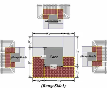
Fig. 3. Our practical range constraints for pin-out. The side restriction will be converted into the RangeSide constraint where pin-blocks are located in RangeSide1, 2, 3 and 4 (each individual shaded region) when the corresponding components are in the south, east, north and west of PCB board respectively.
In order to loosen the restriction from the designers and to obtain a better pin-block placement, we have applied the concepts used in floorplanning [11][12][13]and placement[6][8][9]to redefineanew setofconstraintsasfollows.Wedenotethecoreblock(Core), which is usually arranged power/ground pins for core logic, as a pre-placed module. Since these power/ground pins are located beneath the die and at the center of the package, the heat generated from the die can be transferred out through these pins [1]. For the reason of heat dissipation, the core block will be restricted by pre-placed constraint and placed at the center of the pin-out designation. This constraint is shown as follows (Fig. 3 shows w4, wcore, h1, and hcore):
• Rcore = {(x, y)|w4 +1 ≤ x ≤ w4 + wcore, h1 +1 ≤ y ≤ h1 + hcore}
According to the location of components connecting with the pin-blocks,wedefineanew parameterRangeSide for each pin-block instead of placementsidedefined by designers.Fig.3 showsan examplewherethepin-blocksaredefined in RangeSide1 when the corresponding components are located in the south of PCB board. Therefore, all pins constrained in RangeSide1 must be located within the shaded region and routed toward the south to connect with components. Along the same rule, the RangeSide2, RangeSide3 and RangeSide4aredefined for the pin-blocks if the corresponding components are located in the east, north and west of PCB board respectively. The detailed range constraints for each side are listed as follows ((x, y)∈/Rcore):
•RangeSide1=
{(x, y)|1 ≤ x ≤ w4 + wcore + w2, 1 ≤ y ≤ h1 + hcore/2} •RangeSide2=
{(x, y)|w4 + wcore/2+1 ≤ x ≤ w4 + wcore + w2, 1 ≤ y ≤ h1 + hcore + h3} •RangeSide3=
{(x, y)|1 ≤ x ≤ w4 + wcore + w2, h1 + hcore/2+1 ≤ y ≤ h1 + hcore + h3} •RangeSide4=
{(x, y)|1 ≤ x ≤ w4 + wcore/2, 1 ≤ y ≤ h1 + hcore + h3}
Therangeconstraintsdefinethelargerspaceofplacing pin-blocksthan thatconfined by theplacementsidein [7],thusofferthe opportunities of improving pin-out designation. In addition to the optimization issue, the proposed pin-block planners will satisfy all placement constraints including the pre-placed and range constraints to retain the feasibility of package design.
Fig. 4. The illustration of Cyclic Number Set (CNS) representation. Each parenthesis followed by an index represents one RangeSide, and the number set listed within the parenthesis denotes the pin-block groups constrained in that RangeSide. By perturbation, the order of number set will be changed cyclically, then the planner places the pin-blocks along the sequence of number set in this representation.
III. RANGE CONSTRAINED PIN-BLOCK PLANNING WITH SYSTEM INTERCONNECTS OPTIMIZATION As described in the previous section, we will consider the core region (Core) as a pre-placed module which must be placed in the center of the final pin-out. Besides, pin-blocks will be treated as range-constrained modules and located within given rectangular regions such that no pin-blocks are overlapping. This section presents two pin-block planning heuristics. The first one places the pin-blocks by an intuitively random method (called Rand), the other one applies the algorithm similar to simulated annealing (called SA) by using a Cyclic Number Set (CNS) representation. This representation is specially designed for pin-block planning since it can represent the adjacent relationship between blocks and the starting point of arranging pin-out. Both of them can meet range constraints and optimize the location of pin-blocks.
A. Rand Pin-block Planner
In this method, we use the results of [7] as the initialsolution (they can bereplaced by othergrouping configurations).Thismethod eases the restriction of placement side and applies some stochastic procedures with range constraints. In order to avoid the overlap of pin-block location, pin-blocks will be sequentially placed according to the determined placement sequence (order). The detailed algorithm is listed as follows, where the Side is the distribution region and the Order is the placement sequence pre-defined by thedesigners.
1) Calculate the Cost(S) from the pin-out designation (S) 2) repeat:
3) Input the pre-defined Sideand Orderofpin-block groups 4) RangeSide ← Side; Sequence ← Order
5) Randomly select one RangeSide and randomly choose a pin-block group asthefirstgroup in thisRangeSide 6) Randomly decidethefirstpin location ofthechosen group in theRangeSide,then placethepin-block 7) repeat:
8) Locate the rest groups in the RangeSide according to the Sequence determined in step (4) 9) Select the adjacent RangeSide
10) until all pin-block groups are placed
11) Calculate the Cost(NewS) from the new pin-out desig-nation (NewS) 12) If Cost(NewS) −Cost(S) < 0 then S ← NewS
13) until (Time > Maxtime)
In this procedure, only one RangeSide will be selected to change the sequence of groups. The rest of groups constrained in other RangeSide arelocated in thesameorderasthepin configuration chartpre-defined by thedesigners.
B. SA Pin-Block Planner
In order to explore more in the solution space and obtain greater improvement, we propose the second method to optimize the pin-out. First we introduce a special representation for pin-block planning in thismethod,then wedescribethefloorplanning approach.
Fig. 5. Examples of perturbation process. (a) is theinitialconfiguration.(b)isthefirstperturbation case,theRangeSide2 has been selected and the group orders are exchanged in RangeSide2(Step 1).Thefirstpin location ofGroup3 is randomly decided, then the planner places the pins in the selected RangeSide(Step 2 and 3).Finally,thesequenceofthegroupsdefined in theremainderRangeSidewillfollow theupdated CNS (Step 4). (c) and (d) are the other two perturbation cases.
1) The Cyclic Number Set (CNS) Representation:The fundamental problem tofloorplanning orplacementliesin therepresentation of geometricrelationship among modules[2].Based on theconsideration oftheconstraintsand flexibility in pin-block planner, we propose a Cyclic Number Set (CNS) representation. This representation is specially designed for pin-block planning since it can represent the adjacent relationship between blocks and the starting point of arranging pin-out. It can also describe all variables in perturbation. Fig. 4 shows an example, the parentheses followed by an index represent the RangeSide, and those indices I, II, III and IV represent RangeSide1, RangeSide2, RangeSide3 and RangeSide4 respectively. Pin-block groups which are constrained in each RangeSide are denoted as a number set within the parenthesis. Moreover, the placement sequence of pin-blocks is determined by the order of number set. For instance, the location of pin-blocks shown in Fig. 4 will be represented as CNS=(1)I(2, 3)II(4)III(5, 6)IV. It presents that RangeSide1isthefirstRangeSide randomly selected by theplanner,and thefirstgroup to beplaced in thisRangeSideisgroup1. RangeSide2, the next selected RangeSide, contains two groups where the placement order is group2, group3. RangeSide2 follows the RangeSide1, RangeSide3 follows the RangeSide2, and so forth.
Unlikeotherrepresentationsin floorplanning/placementwhich arecomplicated and inapplicableforpin-block planning, the CNS representation describes the physical region and the relationship among pin-blocks. Once the CNS has been determined based on designer input, the planner can easily place the pin-blocks. Compared with the pin-block floorplannerin [7](information from theauthors),which used 2-D array to storethelocationsforallpins,ourplannercan simply and efficiently transform the representation to real pin-block placement. 2) Simulated Annealing Based CNS Floorplanning: The features of CNS presented above simplify the transformation between representation and pin-block placement. They also facilitate the optimization of pin-block planning in our simulated annealing (SA) based algorithm. The optimization process is described as follows:
Solution Perturbation and Neighborhood Structure
Step 1: Randomly select one RangeSide from the CNS of initial (or previous) solution.
–Move: Randomly choose two groups in this RangeSide, then exchange their sequence. Step 2:Randomly decidethefirstpin location oftheupdated firstgroup then placethepin-block.
Step 3:Therestgroupsdefined in theselected RangeSidewillbe placed along the updated sequence determined in previous move. Step 4:Theremainderofthegroupsdefined in theotherRangeSidewillbeplaced according to thesequencedetermined in previous
solution.
Fig. 6. Estimations of the cost for RangeSide1. The cost/penalty is the placement deviation induced when pin-blocks are placed away from thedefined region (Xl ≤x ≤Xr). By minimizing the total cost, the pin-blocks will be located near the center boundary which is the preferred region for IPs in package design, and the wirelength in PCB escape routing will be reduced.
To produce a feasible solution, after randomly selecting one RangeSide from the CNS of previous solution, it will randomly choose two groups in the selected RangeSide and swap their sequence thus modify the CNS. The rest of steps will proceed depending on the perturbed CNS. Fig. 5 shows the examples of perturbation processes, (a) is the initial/previous solution and the placement of pin-blocks starts from group1 in RangeSide1. Since the RangeSide has been perturbed, the planner revises the CNS and the placement will be reinitiated from RangeSide2 as shown in Fig. 5(b). According to the move, the group orders in RangeSide2 areexchanged (firststep). Next,thefirstpin location ofgroup3 is randomly decided, and the planner places the pins of group3 and group2 (second and third steps). After those steps, the rest groups must be located along the range constraints and the sequence described in the perturbed CNS (fourth step).Finally,ourmethod willgenerateanew CNS ofmodified pin-block location fornextiteration (fifth step).Fig.5(c)and (d)show the other two perturbation cases.
Annealing Schedule: our SA planner uses the following schedule to minimize the cost function, then obtains an optimized pin-out.
–T0 = 100; α =0.9; M =5; Maxtime = 500.
where T0is the initial temperature, αisthecooling rate,M representsthetimesuntilthenextparameterupdate,and Maxtime is the total allowed time for the annealing process. After we obtain the initial solution, the perturbation procedure described above will be invoked to perturb this given solution, then get the new solution which has the minimum cost. The annealing process proceeds iteratively to obtain the best cost.
The major difference between these two methods is the perturbation process. The Rand planner optimizes the cost by iteratively changing the group sequence within one RangeSide. For the remainder of pin-blocks in the other RangeSide, it keeps the same order without the perturbation process. On the contrary, the SA planner will proceed perturbation for the order of pin-block groups in selected RangeSide, then the rest groups will follow the sequence of previous optimized solution and obtain larger improvement.
C. Optimizing Objective Function
For the purpose of optimizing the pin-out designation, we formulate the penalty term which is the deviation of desired pin-block location as our cost function. Its valueisthesquareofthedistanceestimatebetween thepin location and thedefined placementboundary.Asshown in Fig.6,designercan defineamorepreciseboundary forassigning pinsaccording to thefloorplan ofcorresponding IPs.Therefore, those pins will obtain zero penalty when they are placed within the preferred region (Xl≤ x ≤Xr). The detailed estimation of penalty term in RangeSide1 is formulated as follows:
Region 1: Penalty =(|y| + |w4 −Xl|)2when 1 ≤ x ≤ w4, 1 ≤ y ≤ (h1 + hcore/2) Region 2: Penalty = |x −Xl|2when w4 +1 ≤ x ≤ Xl, 1 ≤ y ≤ h1
Region 3: Penalty =0 when Xl ≤ x ≤ Xr, 1 ≤ y ≤ h1
Region 4: Penalty = |Xr −x|2when Xr ≤ x ≤ (w4 + wcore + w2), 1 ≤ y ≤ h1
Region 5: Penalty =[|Xr −(w4 + wcore + w2)| + |y −h1|]2when (w4 + wcore + 1) ≤ x ≤ (w4 + wcore + w2), (h1 + 1) ≤ y ≤ (h1 + hcore/2)
TABLE I THE SUMMARY OF FIVE TEST CASES WHICH HAVE ENTIRELY DIFFERENT CHARACTERISTICS. THE GROUP NUMBER IS THE AMOUNT OF INTERFACES BETWEEN CHIPSET AND INDIVIDUAL COMPONENTS.
TABLE II COMPARISONS OF PENALTY TERM (PLACEMENT DEVIATION) FOR [7], Rand AND SA PIN-BLOCK PLANNERS. THE RESULTS SHOW THAT OUR APPROACHES BOTH HAVE SIGNIFICANT IMPROVEMENT IN
ALMOST ALL TEST CASES (“Imp.”IS THE IMPROVEMENT ON THE PENALTY TERM).
By minimizing the total cost, our methodology not only decreases the signal-net length but also locates the pin-blocksnearthedefined boundary. Therefore, the pin-block planner achieves the requirements of shorter path length and length-matching on package design and PCB routing.
As described in thedefinition ofRangeSide,signalpinslocated in RangeSide1 will route nets toward the south of PCB board then connectwith thecomponents.Hence,when ouralgorithm isfinding theminimum cost,itisto drivethepin-blocks to move to the center of RangeSide1 thus theoretically minimize the signal-net length. Therefore, the optimized pin-out designation will be evaluated by means of
Experimental results are presented as the comparisons of the Rand and SA pin-block planners with our implementation for in [7]. We set the same iteration time (Maxtime) in Rand and SA planner. Although the SA planner needs more runtime, the results shown in Table II demonstrate that the SA planner is better than others in average. Table II also shows that Rand and SA planner both have positive improvementin penalty term when compared with thatin [7],and theruntimeofdesignating and optimizing finalpin-out for all test cases is less than ten minutes. For the design which has enormous pin-block groups, our approachescan obtain thesignificantimprovement1. In order to show theefficiency ofourpin-block location representation, we implement the method in [7] with CNS. Table III shows that the pin-block plannerwillwork efficiently by using CNS representation.
IV. EXPERIMENTAL RESULTS
We have implemented our methodology in C++ and the platform is on Intel Pentium M 1.7GHz with 512MB memory. Five industrial chipset cases, which act as bridges of all components on motherboard are used as our benchmarks (shown in Table I). In the experiments, the penalty term (in Section III.C) which is the placement deviation is considered as our cost function. For the reason of acquiring shorter path length and length-matching on packagedesign and PCB routing,designercan define a preferred region then force the pin-blocks to be planned in that boundary by minimizing the penalty term. In our experiments, we set the center area of each package side as the preferred region as shown in Fig. 6.
1
We observe that the results of our two improved methods are identical in test case I and II. That is because those two test cases have fewer group number, the improved planners have less margins to minimize the cost.
Fig. 7. The wirelength estimate for RangeSide1. The wirelength is calculated in Manhattan distance from signal pin to the reference line (dotted line on the bottom).
calculating the performance metric, the total wirelength. Fig. 7 shows an example of wirelength estimation for pins located in RangeSide1. It is estimated in Manhattan distance from signal pin to the reference line (indicated in a dotted line) of each package side. The wirelength estimates for RangeSide1 are listed below:
Region A: WireLength = |x| + |y|when 1 ≤ x ≤ w4, 1 ≤ y ≤ (h1 + hcore/2) Region B: WireLength = |y|when (w4 + 1) ≤ x ≤ (w4 + wcore + w2), 1 ≤ y ≤ h1
Region C: WireLength = |x −(w4 + wcore + w2 + 1)| + |y|when (w4 + wcore + 1) ≤ x ≤ (w4 + wcore + w2), (h1 +1)≤ y ≤ (h1 + hcore/2)
According to thedefinition ofRangeSide, the reference lines used for calculating the wirelength in RangeSide2, RangeSide3 and RangeSide4 will be established in the east, north and west of package individually. The results of wirelength estimation are shown in Table IV. Again, in most cases Rand and SA planners both have positive improvements over [7] by minimizing total cost. However, there are negative improvements produced by our planners in test case I. Because the pin-block size and group number in each RangeSide are varied, in our planners all pin-blocks will be located near each center of RangeSide to optimize the package performance for high speed IPs. In this case the wirelength will be increased slightly due to the compromise between penalty of each RangeSide.
Fig. 8 shows the pin-out designation of test case I. The pin-out planner of [7] places the most pins of group3, group5 and group6 at thepackagecornerasshown in Fig.8(a),thuscausesthedifficulty in achieving thesignalintegrity ofpackagedesign.Fig.8(b) shows the optimized results, each group move to the center area of RangeSide. The results shown in Table II and IV indicate that in most cases our methodologies not only consider the package design but also minimize the wirelength in PCB escape routing.
V. CONCLUSION
We have proposed two improved pin-block planners with range constraints and a representation for automating pin-out designation. Based on the method of pin-block design in [7], our approach minimizes the package size and considers SI, PI and RA as that in [7]. The experimental results show thattheproposed methodologiesprovidesignificantimprovementespecially forlargenumberofpin-block groups. Furthermore, we can use the range concept to restrict the pin-block location within the preferred region thus optimize the package performance and board wire-planning.
REFERENCES
TABLE III THE EFFICIENCY OF OUR CNS REPRESENTATION ON [7]. THE RESULTS SHOW THAT THE CNS REPRESENTATION CAN FACILITATE THE PLACEMENT OF PIN-BLOCKS EFFECTIVELY.
TABLE IV COMPARISONS OF WIRELENGTH WITH APPROACHES IN [7], Rand AND SA PIN-BLOCK PLANNERS. THE RESULTS SHOW THAT OUR TWO IMPROVED METHODS BOTH HAVE POSITIVE IMPROVEMENT OVER [7] EXCEPT THE
TEST CASE I(”Imp.”IS THE IMPROVEMENT ON THE TOTAL WIRELENGTH ”WL”).
Fig. 8. The results of pin-out designation in test case I (CNS=(1)I (2, 3)II (4, 5)III (6)IV ). (a) is generated by [7], where the group3, group5 and group6 are located at the corner of package. (b) is optimized by SA planner, each group will move to the center of package which is the preferred location for high performance package design.
[2] Y.-C. Chang, Y.-W. Chang, G.-M. Wu, and S.-W.Wu.“B*-Trees: A New Representation for Non-Slicing Floorplans”.In Proceedings IEEE/ACM Design Automation Conference, pages 458–463, 2000.
[3] S.-S. Chen, W.-D. Tseng, J.-T. Yan, and S.-J.Chen.“Printed CircuitBoard Routing and PackageLayoutCodesign”.In Proceedings of IEEE Asia-PacificConferenceon Circuitsand Systems, pages 155–158, 2002.
[4] T.-O. Chong, S.-H. Ong, T.-G. Yew, C.-Y.Chung,and R.Sankman.“Low CostFlip Chip PackageDesign ConceptsforHigh Density I/O”.In Proceedings of IEEE Electronic Componenets and Technology Conference, pages 1140–1143, 2001.
[5]A.Hasan and D.Sato.“BGA PackageBallField Interaction with Manufacturing and Design”.In Proceedings of IEEE Electronic Componenets and Technology Conference, pages 326–333, 2004.
[6] Y.-H. Jiang, J. Lai, and T.-C.Wang.“ModulePlacementwith Pre-Placed Modules Using the B*-Tree Representation”.In Proceedings Internationl
Symposium on Circuits and Systems, pages 347–350, 2001.
[7] R.-J. Lee, M.-F. Lai, and H.-M. Chen. “Fast Flip-Chip Pin-Out Designation Respin by Pin-Block Design and Floorplanning for Package-Board Codesign”.In ProceedingsIEEE Asia and South PacificDesign Automation Conference, pages 804–809, 2007.
[8] J.-M. Lin, H.-E. Yi, and Y.-W.Chang.“ModulePlacementwith Boundary ConstraintsUsing B*-trees”.In IEE Proceedings–Circuits, Devices and Systems, pages 251–256, 2002.
[9]H.Murata,K.Fujiyoushi,S.Nakatake,and Y.Kajitani.“Rectangle-Packing-Based ModulePlacement”.In Proceedings IEEE/ACM International Conference on Computer-Aided Design, pages 472–479, 1995.
[10] A.-H. Titus and B. Jaiswal. “A Visualization-Based Approach for Bump-Pad/IO-Ball Placement and Routing in Flip-Chip/BGA Technology”.In IEEE Transactions on Advanced Packaging, volume 29, pages 576–586, Aug. 2006.
[11] F.-Y. Young and D.-F.Wong.“Slicing Floorplanswith Pre-Placed Modules”.In Proceedings IEEE/ACM International Conference on Computer-Aided Design, pages 252–258, 1998.
[12] F.-Y. Young, D.-F. Wong, and H.-H.Yang.“Slicing Floorplanswith Boundary Constraints”.In IEEE Transactions on Computer-Aided Design of Integrated Circuits and Systems, volume 18, pages 1385–1389, Sep. 1999.
[13] F.-Y. Young, D.-F. Wong, and H.-H.Yang.“Slicing Floorplanswith RangeConstraint”.In IEEE Transactions on Computer-Aided Design of Integrated Circuits and Systems, volume 19, pages 272–278, Feb. 2000.
[14] M.-F. Yu and W.-M.Dai.“Single-LayerFanoutRouting and Routability AnalysisforBallGrid Arrays”.In Proceedings IEEE/ACM International Conference on Computer-Aided Design, pages 581–586, 1995.

![Fig. 2. Two results of pin-b l oc k floor pl a nni ng. ( a ) s hows t he r e s ul t of [ 7] , i t wi l l c ause the longer wirelength (the darker lines) in PCB escape routing when the pin-blocks are not located within the appropriate region](https://thumb-ap.123doks.com/thumbv2/9libinfo/8009868.160382/2.918.270.650.112.437/results-wirelength-escape-routing-blocks-located-appropriate-region.webp)


![TABLE II COMPARISONS OF PENALTY TERM (PLACEMENT DEVIATION) FOR [7], Rand AND SA PIN-BLOCK PLANNERS](https://thumb-ap.123doks.com/thumbv2/9libinfo/8009868.160382/7.918.98.817.444.602/table-comparisons-penalty-term-placement-deviation-block-planners.webp)

![TABLE IV COMPARISONS OF WIRELENGTH WITH APPROACHES IN [7], Rand AND SA PIN-BLOCK PLANNERS](https://thumb-ap.123doks.com/thumbv2/9libinfo/8009868.160382/9.918.247.719.414.1074/table-comparisons-wirelength-approaches-rand-pin-block-planners.webp)
