國
立
交
通
大
學
電控工程研究所
碩
士
論
文
功率消耗模型及模組設計最佳化
運用在積分三角類比數位轉換器
Power Consumptions Model and Model-based
Design Optimization for Sigma-Delta Modulators
研 究 生:黃瑞祺
指導教授:陳福川 教授
功率消耗模型及模組設計最佳化
運用在積分三角類比數位轉換器
Power Consumptions Model and Model-based
Design Optimization for Sigma-Delta Modulators
研 究 生:黃瑞祺 Student:Ray-Chie Huang
指導教授:陳福川 Advisor:Fu-Chuang Chen
國 立 交 通 大 學
電 控 工 程 研 究 所
碩 士 論 文
A ThesisSubmitted to Department of Electrical and Control Engineering College of Electrical Engineering and Computer Science
National Chiao Tung University in partial Fulfillment of the Requirements
for the Degree of Master
in
Electrical and Control Engineering
August 2009
Hsinchu, Taiwan, Republic of China
功率消耗模型及模組設計最佳化
運用在積分三角類比數位轉換器
研究生:黃瑞祺 指導教授:陳福川 教授 國立交通大學 電控工程研究所摘要
傳統的積分三角類比數位轉換器系統設計是一個相當耗時的工作,需要不斷的嘗試各 種系統參數,以達到所需要的解析度以及功率消耗要求。本篇論文分析了積分三角類比 數位轉換器的主要雜訊來源與非線性特性所造成的失真問題。藉由分析推導出的失真功 率模型、雜訊功率模型及絕對功率消耗模型,並以訊號對雜訊和失真比(SNDR)來當作 我們的設計規格,以做最佳化的設計。此最佳化設計意指在某特定系統規格下,找到一 組最佳化的系統參數,使得類比數位轉換器的功率消耗最小以及訊號對雜訊和失真比最 大,並節省龐大制定系統參數的時間成本。最後我們將針對已發表的設計結果來做驗證 的工作。雖然現今已存在相當多行為模擬工具以自動化制定系統參數,但相較之下,本 論文所提出的數學式最佳化方法將快上許多。Power Consumptions Model and Model-based
Design Optimization for Sigma-Delta Modulators
Student:Ray-Chie Huang Advisor:Dr. Fu-Chuang Chen
Institute of Electrical and Control Engineering Nation Chiao Tung University
ABSTRACT
The conventional sigma-delta ADC system design is a time consuming process and needs much trials and errors with system parameters(GBW, OSR and Bit…etc ) to meet the specific specifications(signal bandwidth, SNDR). This paper analyze the mainly noise sources and nonlinear distortions. Utilizing the noise power models, nonlinear distortion power models and accurate power consumption models derived in this paper, and the assigned signal to noise and distortion ratio (SNDR) to be the design goal, we can forward to do design optimization under the specific specifications. Design optimization means that under the specific specifications, we find a set of optimal design parameters such that the power consumption of ADCs is minimum and SNDR is maximum, and reduce the huge time-cost to set up the circuit specifications. Finally, design optimization is tested against a published design result. Although design automation issues have been partially addressed by recent behavior- simulation–based methods, yet such methods can be slower than our analytical approach far.
Contents
中文摘要……….I English Abstract………...II Contents………....III Lists of Tables………....V Lists of Figures………...VI List of Symbols………..VIII Chapter1 Introduction………..11.1 Current Status and Background……….1
1.2 Motivation and Aims……….1
1.3 Organization………..2
Chapter2 Fundamental Theorems of Sigma-Delta Modulators………...3
2.1 Nyquist Sampling Theorem………3
2.2 Quantization Noise and Peak SNR……….5
2.3 Techniques of Sigma-Delta Modulator………...7
2.3.1 Oversampling Technique……….7
2.3.2 Noise shaping………..9
2.4 Architectures of Sigma-Delta Modulator………..11
2.4.1 First-Order Sigma-Delta Modulator………..12
2.4.2 Single-Loop Second-Order Sigma-Delta Modulator……….13
2.4.3 Single-Loop High Order Sigma-Delta Modulator……….15
2.4.4 Interpolative Sigma-Delta Modulator………...16
2.4.5 MASH Architecture………...17
2.4.6 Multi-bit Quantizer Sigma-Delta Modulator...18
2.4.8 Decimator………...21
2.4.9 Performance Metrics for a ΣΔ Modulator……….21
Chapter3 Models of Sigma-Delta Modulator Noises Power………...24
3.1 Clock Jitter Effects………...24
3.2 Thermal noise (Switch circuits) ………..25
3.3 Finite OTA Gain Error……….26
3.4 Multi-bit DAC noise……….27
3.5 Settling noise………28
3.5.1 Variance equation of VS……….29
3.5.2 Settling noise power of integration phase………..30
3.5.3 Dependence with settling noise and quantization noise………33
Chapter4 Models of Sigma-Delta Modulator Power Consumption………..35
4.1 Static Power Consumption………....35
4.1.1 OTA power model………..36
4.1.2 Comparator power model………...39
4.2 Dynamic Power Consumption………..39
4.2.1 Switch power model………..40
4.2.2 DAC power model……….41
4.2.3 Digital power model………..43
Chapter5 Design Optimization of Sigma-Delta ADCs Design………46
Chapter6 Conclusions and Future Works……….48
Lists of Tables
TABLE 3.1 Coefficient of polynomial……….30
TABLE 4.1 power dissipation between Static part and Dynamic part in different bit………..35
TABLE 4.2 Value of ζ0 and ζ1 in different amplifier………..38
TABLE 4.3 Relationship between power models and system parameters………...45
TABLE 5.2 The representation of each noise in our models………47
Lists of Figures
Fig. 2.1(a)Original signal spectrum (b)Sample function when fs > 2fB
(c)Signal spectrum that is sampled by (b) (d)Sample function when fs < 2fB
(e)Signal spectrum that is sampled by (d) ………4
Fig. 2.2 Quantization process……….5
Fig. 2.3 Quantization error caused by A/D converter……….5
Fig. 2.4 Quantization error range………...6
Fig. 2.5 P.D.F of quantization error………6
Fig. 2.6 Sampling system………...8
Fig. 2.7 Noise distribution after sampling………...8
Fig. 2.8 (a)General ΣΔ modulator (b)Linear model with quantization noise………....9
Fig. 2.9 Noise shaping………...10
Fig. 2.10 Block diagram of A/D converter………...11
Fig. 2.11 First-order modulator……….12
Fig. 2.12 Single-loop second order ΣΔ modulator………...14
Fig. 2.13 Comparison of noise shaping techniques………..15
Fig. 2.14 Single-loop high order ΣΔ modulator………...16
Fig. 2.15 Four-order interpolative architecture………...16
Fig. 2.16 2-1 architecture MASH ΣΔ modulator……….…..17
Fig. 2.17 SNR vs. OSR with different quantizer bit number………....18
Fig. 2.18 Multi-bit architecture……….……19
Fig. 2.20 Performance characteristic of a converter……….23
Fig. 3.1 Main nonidealities sources in the ΣΔ modulator………..25
Fig. 3.2 Histogram distribution of Vs(n) ………..29
Fig. 3.3 Three types of settling conditions in integration phase………...31
Fig. 4.1 Structure of OTA………..36
Fig. 4.2 Simulation of OTA power model……….38
Fig. 4.3 CMOS transmission gate………...40
Fig. 4.4 Sampling phase……….42
Fig. 4.5 Integration phase………..42
Fig. 4.6 CMOS logic inverter………..44
Fig. 5.1 Flow of the proposed optimization for the ΣΔ modulator Model-based design………...46
List of Symbols
Symbols
LSBV Quantizer step size
OS
V Maximum output swing of op-amp OSR OverSampling Ratio
ΣΔ
k
Order of the Sigma-Delta modulatorB Number of bits in the quantizer
S f Sampling Frequency B f Signal Bandwidth ref V
Reference Voltage of the quantizer
0
A Finite Gain of OTA
in
f Frequency of the input signal
i
φ ith phase of a nonoverlap clock
in
A Amplitude of input signal
jit
σ
standard deviation of clock jitter
S
C Sampling capacitor
I
C Integrating capacitor
L
C Load capacitor of OTA
gate
C
The loading capacitors of CMOS logic gates
Switch
OX
C The capacitance per unit area of the gate oxide
S
V Input signal plus feedback DAC signal
1
τ Time constant of input branch
VS
σ Standard deviation of VS
2
τ Time constant of integrator output settling
i
a gain coefficient of th integrator i
η percentage of the bottom plate parasitic
T Absolute temperature Switch R Switch ON resistance N quantizer levels m G Amplifier transconductance Pr() Probability of some condition
k Boltzmann’s constant (1.38×10⁻²³) J/K
α OTA noise factor []
Erf Error Function
OTA
I Total current of the OTA
BASE
I Base current of each transistor of the input differential pair of OTA
OTA
K The ratio of the total current of the OTA to this bias current
2
cl
f The GBW of the OTA
reff
V The overdrive voltage of the transistor of the input differential pair of OTA
0
1.
Introduction
1.1 Current Status and Background
The sigma-delta modulator based on switched-capacitor circuits is well suited for high resolution medium-to-low-speed applications such as digital audio [1-2][3-6], voice codec [7], and DSP chip. Recently, with the popularity of the portable devices, the low power devices became a very important topic [4]. To reduce power consumption is to extend the life of the battery and to bring the convenience to the users. Design optimization towards minimal power consumption is popular with the high-speed low-power applications of the ΣΔ modulator [8-14]. ADCs have been frequently applied to higher signal bandwidth, and low power consumption designs. For example, in xDSL [15-16], WiMAX [17-18] and WLAN [19] applications, signals up to several MHz must be handled. When signal bandwidth increased, the power dissipation will increased too. Both of them are trade of specification, so how to reduce power consumption and increase resolution were important issue of Sigma-Delta A/D converters design.
ΣΔ
1.2 Motivation and Aims
The power consumption of the Sigma-Delta A/D converters is important in all kinds of application. So it is difficult that how to design can get the better power consumption. We propose a power consumption model to estimate the power consumption in the discrete time ADCs design. Generally, the OTA (Operational Transconductance Amplifier) are the components consuming the most power in SDM [5]. The OTA power consumption model also the most difficult to estimate cause it has three system parameters (GBW, SR and DC-gain) in this power consumption model. Since significantly increasing the sampling rate
and reduce power consumption is difficult [4], designers seek DC-gain in order to achieve low power consumption and high-linearity. Due to the complexity with OTA, the papers about OTA noise and distortion can’t directly offer an efficient method to obtain optimum DC-gain in low power consumption required. How to choice an optimum equilibrium of power consumption and resolution is important to designers. To propose the design optimization forΣΔ modulators, we need a complete set of important nonideality models and the power consumption model. The performance of the ΣΔ ADCs is usually expressed in terms of SNR and SNDR. Circuit designers must take into consideration the nonidealities and decide the circuit and system parameters to meet the desired specifications. A design optimization procedure is proposed to meet design specifications while minimizing power consumption. In a modulator, common causes for harmonic distortions are nonlinear finite DC-gain,
settling error, nonlinear capacitances, quantizer nonlinearity, nonlinear switch resistance and unit-DAC mismatch. OTA are the critical part of the
ΣΔ
ΣΔ modulators and its nonidealities such as nonlinear finite DC-gain and settling error may produce distortions and noise significantly. With these models for design optimization, we can increase the automation and reduce complexity in the single-loop ΣΔ ADCs design.
1.3 Organization
This work is organized as follows. In Chapter 2, systematic studies of fundamental theory and various architectures of modulator are presented first. The total noise power of Sigma-Delta Modulator has a brief introduction in Chapter 3. The accurate power consumption models is derivedin Chapter 4. A design optimization scheme is proposed in Chapter 5.. Conclusions and future works are presented in Chapter 6.
2.
Fundamental Theorems and Architectures of
Sigma-Delta Modulators
Before we establish the OTA gain distortion model of ΣΔ modulators, several important theorems and concepts must be known, such as Nyquist sampling theorem, quantization error and the two most critical techniques in a ΣΔ modulator: oversampling and noise shaping. All topologies of ΣΔ modulators are based on these two techniques. There also have some parameters we must to understand, such as OSR, SNR, and SNDR …etc. This chapter starts from fundamental theorems, and introduces several topologies of ΣΔ modulators.
We will illustrate quantization error and analyze quantization noise in an ideal A/D converter and then derives the peak signal-to-noise ratio. The resolution of an A/D converter is determined by signal-to-noise ratio, which is a very important specification in an A/D converter.
2.1 Nyquist Sampling Theorem
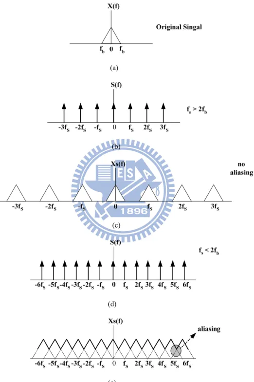
In an analog-to-digital converter, the analog signal from external environment must be converted to discrete-time signal by sampling. However, the sampling rate (fs) and signal bandwidth (fB) must follow the Nyquist sampling theorem in (2.1):
f
S ≧ 2f
B (2.1)The sampling rate must be higher or equal to twice of signal bandwidth in order to prevent from aliasing. We will illustrate the phenomenon of aliasing by Fig. 2.1. Fig. 2.1(a) and (b) are the spectrums of signal and sample function respectively; from fig. 2.1(c), when sampling rate is twice higher than signal bandwidth, the signal after sampling has no aliasing and it can be perfectly reconstructed by using low pass filters. However, in Fig. 2.1(d), when the
sampling rate is lower than twice of signal bandwidth, aliasing will appear in the signal after sampling. The signal having aliasing is difficult to reconstruct to original signal, like Fig. 2.1(e). (a) (b) (c) (d) (e)
Fig. 2.1(a)Original signal spectrum(b)Sample function when fs > 2fB(c)Signal spectrum that' sampled by (b)(d)Sample function when fs < 2fB(e)Signal spectrum that sampled by (d)
2.2 Quantization noise and Peak SNR
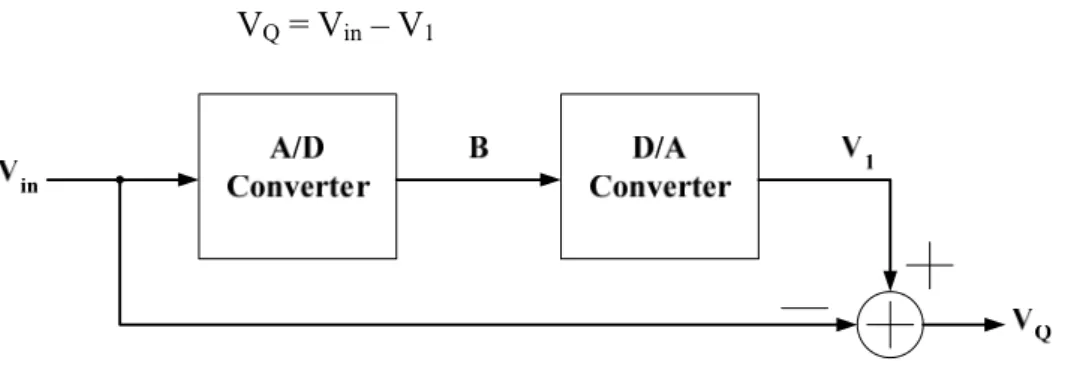
We can get a discrete-time signal by sampling a continuous-time signal, and this sampled signal can be converted to digital signal. Quantization will appear in this process, the basic concept of quantization is to classify the original signal to different levels according to its level to determine the bit number of this signal, as shown in Fig. 2.2
Fig. 2.2 Quantization process
It will have quantization error even in an ideal analog-to-digital converter. As shown in Fig .2.3, we convert the digital signal B to analog signal V1 by a D/A converter, and then the
signal V1 is subtracted by input signal Vin. The result is the quantization error VQ, as in (2.2)
[20].
VQ = Vin – V1 (2.2)
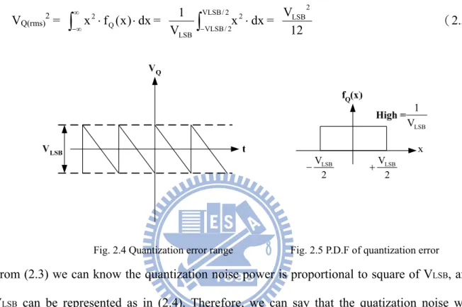
The range of quantization error is limited in ±VLSB/2 (as in Fig. 2.4), and we assume the
probability density function of quantization error is uniformly distributed between ±VLSB/2
and its mean is zero, as shown in Fig. 2.5. From this assumption, we can easily get the quantization noise power VQ(rms)2 in (2.3).
VQ(rms)2 =
∫
= ∞ ∞ − x ⋅fQ(x)⋅dx 2∫
− ⋅ 2 / VLSB 2 / VLSB 2 dx x V 1 LSB = 12 VLSB2 (2.3) 2 VLSB + 2 VLSB − LSB V 1Fig. 2.4 Quantization error range Fig. 2.5 P.D.F of quantization error
From (2.3) we can know the quantization noise power is proportional to square of VLSB, and
VLSB can be represented as in (2.4). Therefore, we can say that the quatization noise will
reduce by increasing quantization bit number. VLSB = B
2 FS
(2.4) FS=Full scale = Vref+-Vref- B:Quantization bit number
Assume that input signal is sinusoidal, expressed as Vin(t) = A sinωt, so the input signal
power Vin(rms)2 is as (2.5). In (2.5), we define the amplitude of input signal is the full scale
of reference voltage, and from (2.3), (2.4) and (2.5), the peak SNR(Peak Signal-to-Noise Ratio) can be derived as in (2.6).
Vin(rms)2 =
∫
− ⋅ ⋅ 2 / T 2 / T 2 dt ) t sin A ( T 1 ω = 2 A2 = 8 ) A 2 ( 2 = 8 FS2 (2.5) PSNR = 10 log( 2 ) rms ( Q 2 ) rms ( in V V )= 6.02B + 1.76 dB (2.6)(2.6) is the result obtained by Nyquist sampling rate. From (2.6), we can know that each additional bit number in quantizer increases 6dB in SNR. In Nyquist A/D converters, increasing the resolution of quantizer (decrease VLSB) while reducing the quantization noise is
a general method to reach higher SNR, but this method is sensitive to mismatches of analog device. Therefore, the general Nyquist A/D converter is not easily to implement with high resolution.
2.3 Techniques of Sigma-Delta Modulator
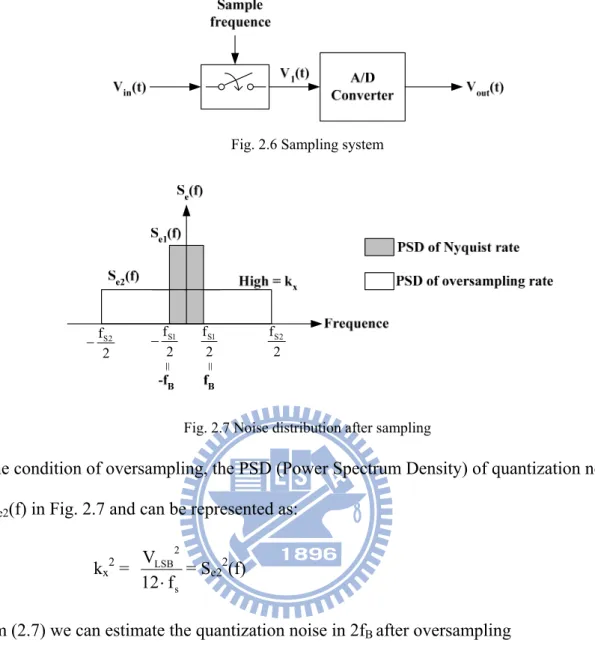
ΣΔ A/D converters are based on oversampling and noise shaping to reach high resolution. Oversampling means the sampling rate is much higher than Nyquist rate, about 8~512 times in general applications. The goal of oversampling is to expand quantization noise to wider range. It can reduce the quantization noise in signal bandwidth and increase the DR (Dynamic range) of input signal. Noise shaping is a technique that moves noise to high frequency, which is done by using discrete time filter and feedback technique. After noise shaping, the noise in high frequency can be filtered out by a digital filter [21].
2.3.1 Oversampling Technique
First, we made the assumption that quantization noise is a uniform distribution in sampling spectrum so its mean is zero and is a white noise [22]. The system in Fig. 2.6 just has oversampling function and does not have noise shaping effect. If a A/D converter is sampled in Nyquist rate, then the quantization noise is uniform distributed between ±fB ; if it
is sampled by oversampling technique, then quantization noise is uniform distributed between± fS2/2s, which is much larger than fB. As shown in Fig. 2.7, if the signal bandwidth is
between ±fB, then quantization noise in this bandwidth will be reduced by using oversampling
Fig. 2.6 Sampling system 2 fS1 2 fS1 − 2 fS2 2 fS2 −
Fig. 2.7 Noise distribution after sampling
In the condition of oversampling, the PSD (Power Spectrum Density) of quantization noise is as Se2(f) in Fig. 2.7 and can be represented as:
kx2 = s 2 LSB f 12 V ⋅ = Se2 2(f) (2.7)
From (2.7) we can estimate the quantization noise in 2fB after oversampling
PQ =
∫
= − ⋅ B B f f 2 x df k OSR 2 12 FS 12 V f f 2 B 2 2 2 LSB S B ⋅ ⋅ = ⋅ (2.8)In (2.8), we define a parameter OSR (Oversampling Ratio) as OSR = B S f 2 f (2.9)
Finally, we can get PSNR from (2.5) and (2.8)
PSNR = 10 log( Q signal P P )= 6.02B + 1.76 + 10 log(OSR) (2.10)
From (2.10), we can find that doubling OSR will increase 3dB in PSNR, which is about 0.5 bit increase in resolution. Although oversampling can reduce quantization noise, it is difficult
to reach high SNR when using a low bit quantizer. For example, if we need a 16bit A/D converter, then SNR must be equal to 98dB, if the signal bandwidth is 20KHz, then the sampling rate must equal to 2 × 109 × 20KHz, it is impossible to implement. Because at such high frequency, quantization noise is no longer a white noise, it is correlated with input signal. So there is not only oversampling technique, we must add noise shaping technique also, if we want to achieve high resolution.
2.3.2 Noise Shaping
We can model a general ΣΔ modulator and its linear model as shown in Fig. 2.8.
H(z) Quantizer y(n) x(n) u(n) (a) (b)
Fig. 2.8 (a) General ΣΔ modulator (b) Linear model with quantization noise
From Fig. 2.8(a), we can derive output Y(z) as (2.11) Y(z) = ) z ( H 1 ) z ( H + X(z) + 1 H(z) 1 + E(z) (2.11) and define Signal Transfer Function STF and Noise transfer function NTF as
STF (z)= ) z ( H 1 ) z ( H ) z ( X ) z ( Y + = (2.12) NTF (z)= ) z ( H 1 1 ) z ( E ) z ( Y + = (2.13)
where H(z) is the transfer function of a discrete time filter. There have two important meanings in (2.12), (2.13). If we want to obtain highest SNR, STF must be equal to 1, that
means the input signal can transfer to output without attenuating; and NTF (z) must be equal to
0, because the quantization noise will not affect output SNR.
In order to make NTF (z) be a high pass filter, so at DC(z = 1), NTF must be 0, and z = 1 is
a pole of H(z), so the transfer function H(z) of the discrete filter is as H(z) = 1 Z 1 − = 1 1 Z 1 Z − − − (2.14) Substitute (2.14) into (2.12) and (2.13), we can get
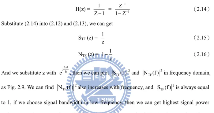
STF (z) = z 1 (2.15) NTF (z) = z 1 1− (2.16)
And we substitute z with fs f 2 j
e
π
, then we can plot STF(f)2 and NTF(f)2 in frequency domain, as Fig. 2.9. We can find NTF(f) 2 also increases with frequency, and STF(f)2 is always equal to 1, if we choose signal bandwidth in low frequency, then we can get highest signal power and lowest noise power, from this figure we see that quantization noise is moved to higher frequency significantly, this is the noise shaping effect.
2 TF(f) N 2 TF(f) S
Fig. 2.9 Noise shaping
After noise shaping, we can filter out the noise in high frequency by using digital filter, and we will illustrate its architecture more detail in the next chapter.
2.4 Architectures of Sigma-Delta Modulator
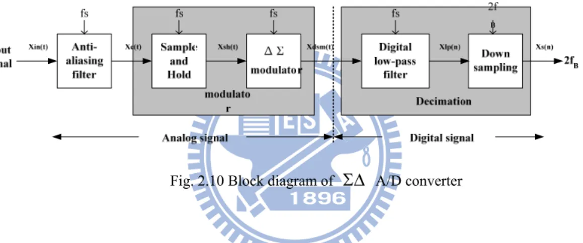
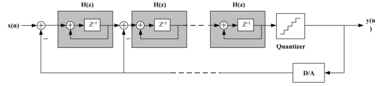
Before we introduce various architectures of ΣΔ modulators, we must to realize the basic architecture of a general A/D converter. Fig. 2.10 is a complete block diagram of a
A/D converter [20], and we can divide it into two different parts. First part is the ΣΔ
ΣΔ ΣΔ
modulator. The main function of this part is doing oversampling and noise shaping to the input analog signal. Second part is the decimation filter. The main function of this part is to remove noise in high frequency and down sampling the sampling frequency to base band frequency.
Fig. 2.10 Block diagram of ΣΔ A/D converter
First, the input signal Xin(t) pass an Anti-aliasing filter, the 3dB frequency of this filter is about few times of Nyquist frequency, so signal and noise out of Nyquist frequency is filtered roughly, and this signal goes into the ΣΔ modulator after goes through a S/H circuit. However, in the circuits implement situation, the sample and hold function is included in the circuits of modulator, so the signal Xc(t) will pass this modulator and produces a high speed data code Xdsm(n), because of noise shaping, the quantization noise will appear in high frequency. Finally, we must filter the noise in high frequency and reduce the sampling frequency to Nyquist frequency by a decimator, and passes the digital signal to the output [20].
ΣΔ
In this chapter, we will focus on the architectures of ΣΔ modulator, because that the noise model and optimal method is focus on this part, we must understand the theorem,
benefits and drawbacks of each kinds of ΣΔ modulators. In addition, the implement of decimator is very typical [23, 24]. In today’s technology, DSP processors are also used to replace decimators, so we will introduce this part roughly.
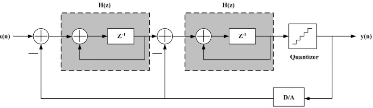
2.4.1 First-Order Sigma-Delta Modulator
We recall that H(z) in (2.14) is 1 1 Z 1 Z − −− , substitute it into Fig. 2.8, then we can get a first-order modulator; Analyze transfer function H(z) from time-domain, it indicates that output signal m(t) is obtained by adding the delayed input signal n(t-1) and the delayed output signal m(t-1), so we can express a complete first-order
ΣΔ
ΣΔ modulator as Fig. 3.2.
ΣΔ modulator
Fig. 2.11 First-order
H(z) in Fig. 2.11 is indicated the effects of delay and accumulation, this is equivalent with an integrator in circuit design, so the three circuits components of ΣΔ modulator are integrator, quantizer and DAC in the feedback path. A first order ΣΔ modulator’s output can represent as Y(z) = z-1X(z) + (1-z-1)E(z) (2.17)
From (2.17) we can find the signal transfer function is as a delay function, and noise transfer function is as a high pass filter, moves the noise to high frequency. In order to derive PSNR of first order ΣΔ modulator, we must get the magnitude of NTF(z) and STF(z) in the frequency
domain, so we substitute z with ej2π⋅f/fs, and get S (f)
TF and NTF(f) respectively as:
s f/f j2π e− ⋅ = 1 TF(f) z S = − = 1 (2.18) NTF(f) = 1-e−j2π⋅f/fs= j f/fs s e j 2 ) f f sin(π × × −π⋅ ⇒ ) f f sin( 2 ) f ( N s TF π ⋅ = (2.19)
So the quantization noise in base band ±fB can obtain by (2.7) and (2.19)
PQ = df f f sin 2 f 12 V df ) f ( N ) f ( S 2 f f s s 2 LSB 2 TF f f 2 e B B B B ⋅ ⎥ ⎦ ⎤ ⎢ ⎣ ⎡ ⎟⎟ ⎠ ⎞ ⎜⎜ ⎝ ⎛ ⋅ ⋅ = ⋅
∫
∫
− − π (2.20)Because that fB is much lower than fs, so sin(π f/fs) is approximate equal to (π f/fs), and PQ is
as PQ = 3 2 2 LSB ) OSR 1 ( 36 V π ⋅ = 2B2 2 3 OSR 2 36 FS ⋅ ⋅ ⋅π (2.21) From (2.5) and (2.21), if we have the maximum signal power, then PSNR is as (2.22)
PSNR = 10 log( Q signal P P ) = 10 log( 22B 2 3 ) + 10 log[ 3 2 (OSR) 3 π ] = 6.02B + 1.76-5.17 + 30 log(OSR) (2.22) From (2.22), we find that each octave of OSR, PSNR will increase 9dB, increase 1.5 bit in resolution. Compare (2.22) with (2.10) that only has oversampling effect; we can find that 1st order noise shaping increases the performance of ΣΔ modulator.
2.4.2 Single-Loop Second-Order Sigma-Delta Modulator
When the discrete time filter in Fig. 2.8 is replaced by two cascade integrator, then it is a second order modulator, output of the first integrator is only connecting with the input of the second integrator, it is shown in Fig. 2.12
Fig. 2.12 Single loop second order ΣΔ modulator
Then the output of it can easily be derived as
Y(z) = z-2X(z) + (1-z-1)2E(z) (2.23)
where STF and NTF is as
STF(z) = z-2 (2.24)
NTF(z) = (1- z-1)2 (2.25)
Using the same method in (2.19) (2.20), we can obtain
STF(f) =1 (2.26) 2 s TF f f sin 2 ) f ( N ⎥ ⎦ ⎤ ⎢ ⎣ ⎡ ⎟⎟ ⎠ ⎞ ⎜⎜ ⎝ ⎛ ⋅ = π (2.27) PQ = 5 4 2 LSB OSR 60 V ⋅ ⋅π = 2B 5 4 2 OSR 60 2 FS ⋅ ⋅ ⋅π (2.28) So finally, PSNR of the second order ΣΔ modulator is as
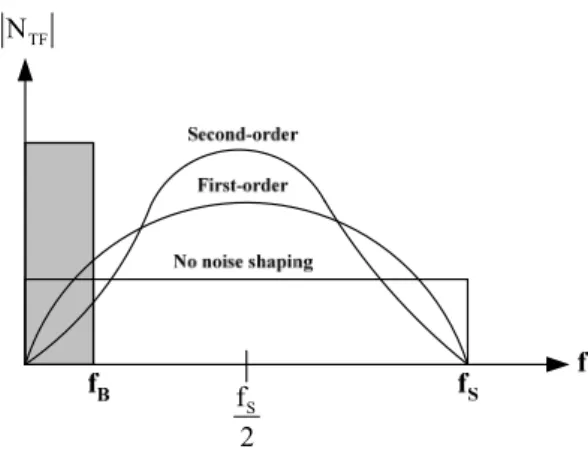
PSNR = 10 log( Q signal P P ) = 10 log( 22B 2 3 ) + 10 log[ 5 4 (OSR) 5 π ] = 6.02B + 1.76-12.9 + 50 log(OSR) (2.29) In the single loop second order architecture, each octave of OSR can increase PSNR by 15 dB, it is equivalent to 2.5 bit in resolution. If we compare (2.29), (2.27) with NTF(f) =1 that without noise shaping, as Fig. 2.13, we can find that in our needed signal bandwidth, the quantization noise is highest when NTF(f) =1, and that with second order noise shaping is
smallest among this figure [20].
TF
N
2 fS
Fig. 2.13 Comparison of noise shaping techniques
2.4.3 Single-Loop High Order Sigma-Delta Modulator
Fig. 2.14 is a single loop high order ΣΔ modulator, from the derivation in Section 2.4.1 and Section 2.4.2, we can get the quantization noise PQ in signal bandwidth is as
PQ = 2L 1 L 2 2 LSB ) OSR 1 ( 1 L 2 12 V ⋅ + + ⋅ π ,L:order (2.30) and its PSNR is PSNR = 6.02B+1.76-10 log( 1 L 2 L 2 + π )+(20L+10) log(OSR) (2.31) In the application of high order ΣΔ modulator, (6L+3)dB increases in SNR when OSR is octave, so PSNR can be raised by increasing the order of the system, especially at large oversampling ratio. But sometimes in high order architecture, the performance will be worsen than result predicted by (2.29), because of the stability problem, it will make less effective noise shaping function, so the quantization noise will not be suppressed completely.
Fig 2.14 Single-loop high order ΣΔ modulator
2.4.4 Interpolative Sigma-Delta Modulator
Interpolative is a kind of high order ΣΔ modulator, it changes connection of some stages, adds some feed forward paths and feedback paths in order to suppose more aggressive noise shaping effect, Fig. 2.15 is a four-order interpolative architecture ΣΔ modulator [16].
1 1 z 1 z − − − 1 1 z 1 z − − − 1 1 z 1 z − − − 1 1 z 1 z − − −
Fig. 2.15 Four-order interpolative architecture
This architecture also has stability problem, when the order L increases, each integrator produces one pole, and when the order is higher, poles of this system will also increase, and it will cause unstable situation, so the range of integrator gain will be limited; if the range of integrator gain is small, oscillation will appear in the circuits. Another is the considerations of clock control, when we use SC (switched-capacitor) to implement the integrator, each integrator needs two clocks to control its operation, and we will need more clock to control the integrator when the order of system increases, it will produce more problems.
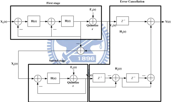
2.4.5 MASH Architecture
MASH (Multi-stage noise shaping) architecture is also called cascade architecture, which is a method that cascades several low order loops modulator in order to get high order noise shaping effect. The fundamental ideal of MASH is delivering quantization noise of front stage to input of next stage, and combining the digital outputs of all the stages with proper transfer function in digital domain, only the quantization noise of last stage will appear at the output, and the orders of NTF is the same with total orders in the cascade ΣΔ modulator. Fig 2.16 is
a three-order cascade modulator, its is the combination of a second-order and first-order modulator, so also called 2-1 cascade architecture.
ΣΔ ΣΔ 1 − Z 1 − Z Z−1
Fig. 2.16 2-1 architecture MASH ΣΔ modulator
From Fig. 2.16, we can derive the first stage output Y1(z) can be represented as
Y1(z) = z-2X1(z) + (1-z-1)2E1(z) (2.32)
Output of second stage Y2(z) is as
Y2(z) = z-1X2(z) + (1-z-1)E2(z) (2.33)
and overall output of MASH Y(z) is as
Y(z) = H1(z)Y1(z) + H2(z)Y2(z) (2.34)
eliminate first stage quantization noise E1(z), from (2.32) ~ (2.34), we can define the error
cancellation functions H1(z) and H2(z) as
H1(z) = z-1 (2.35)
H2(z) = (1-z-1)2 (2.36)
From (2.32)~(2.36), E1(z) can be eliminated, and second stage quantization noise E2(z) is
shaped by third-order noise shaping function, and the MASH output Y(z) is as
Y(z) = z-3X1(z) + (1-z-1)3E2(z) (2.37)
The most significant advantage of this architecture is that stability is not an issue, because it is composed by several low-order systems, and the quantization noise will not be amplified stage by stage, so its stability is good. Most important, the noise shaping function is equivalent as high order modulator, so it is popular in recent publications [25, 26]. However, there also have some drawbacks of this topology; it is sensitive to the circuits' imperfections, such as finite DC gain of OTA, variance of integrator gain due to capacitor mismatch and non-zero switch resistance. These are all practical considerations when we design a MASH architecture modulator [27].
ΣΔ
ΣΔ
2.4.6 Multi-bit Quantizer Sigma-Delta Modulator
The demands of high resolution and high bandwidth ADC are more and more in recent years. In a high signal bandwidth, OSR of ΣΔ ADC can’t be too high, and the peak SNR of a modulator with such limited OSR can’t satisfy of high resolution applications, if we use higher order architecture, then the performance will degrade due to instability. So the most general method to increase performance is to use multibit quantizer. The most obvious advantage of using multibit quantizer is that the distance between quantizer level VLSB in (2.4)
is much smaller due to increasing of B, and according to (2.3), the power of quantization noise is attenuated. Fig. 2.17 is the results of theoretical peak SNR of modulator versus oversampling ratio, with different order and quantizer bits, it is noted that peak SNR of the
ΣΔ
same OSR is increase 6 dB with each additional bit number in quantizer, and at low OSR, low order higher bit number architecture has equivalent performance as high order architecture. This result is usable for high bandwidth applications, and the power consumption of digital circuit in ΣΔ modulator is reduced due to lower sampling rate [28].
0 50 100 150 200 250 300 20 40 60 80 100 120 140 160 OSR S NR O2B1 O2B2 O2B3 O3B1
Fig. 2.17 SNR vs. OSR with different quantizer bit number
Because of using multi-bit quantizer, so we also need to use multi-bit DAC(Digital-to Analog Converter) to transfer the digital output to analog signal, and feed it back to integrator. The most significant disadvantage is the non-linearities introduced by multi-bit DAC can degrade the performance of converter, like Fig. 2.18. It is a linear model of multi-bit modulator, where E(Q) and E(D) represent the quantization noise and feedback DAC noise respectively. The values of these capacitor elements in DAC will not equal to ideal values that we need, it is due to process variation, typical value of mismatch in modern CMOS technology is about 0.05% ~ 0.5%. In recent years, so many researches are make efforts on reduce DAC noise due to mismatch, such as trimming [21], Dynamic element matching(DEM)[29, 30], although trimming is effective, but it has a expensive production step. So, DEM becomes more and more popular because of its efficiency and cheaper cost.
ΣΔ ΣΔ
Fig. 2.18 Multi-bit architecture
2.4.7 Multi-bit Sigma-Delta Modulator use DEM Technique
Dynamic element matching is a different approach to decrease the DAC noise, it is used to improve the linearity of pure DACs [31], but now it is most used in inner DAC of multi-bit modulator. A DAC with DEM technique is illustrated in Fig. 2.19, bits thermometer code is put into the element selection logic block, and the function of element selection logic is try to select DAC elements in such way let the errors introduced by DAC average to zero for several operation periods. Because the DEM block is located in feedback loop, so its delay must be very small prevent to degrade the performance of
ΣΔ 2B
ΣΔ converter, therefore the algorithm used in the DEM block must be simple. There are several techniques of DEM, such as Randomization [32], Clocked Averaging (CLA) [3], Individual Level Averaging (ILA) [33], Data Weighted Averaging (DWA) [3], Randomization is the first approach to use DEM technique in ADC, and DWA offers a good performance to reduce DAC error, in this section, an overview introduction of these two algorithms will be presented, and the operation principle of them will be explained.
1 2B− 1 2 B 2 B 2
Fig. 2.19 A B-bit DAC with DEM technique
2.4.8 Decimator
In ΣΔ A/D converter, digital decimator is used to process digital signal of the quantizer output, the high speed data word after oversampling modulation can’t be used directly. Because there have original signal and quantization noise among it, so the main function of decimator is to convert the oversampled B-bit output words of the quantizer at a sampling rate of fs to N-bit words at Nyquist rate of input, and removes the noise out of signal band. In order to prevent the noise introduced by other frequency, the decimator filter must have very flat signal pass-band, and sharp transition region and enough signal attenuation in stop band. Two-stage decimator is used in a general situation, because that single stage decimator is difficult to convert sampling rate to Nyquist rate in 1 time and without degrading SNR. In the first stage, we can down-sample the sample frequency to 2~4 times of Nyquist frequency, and in the second stage, we can use IIR or FIR filter that have high linearity [21]. For a large OSR, multi-stage decimator is used.
2.4.9 Performance Metrics for a
ΣΔModulator
In order to understand the performance merits used to specify the behavior of ΣΔ modulator, several specifications concerning the performance are discussed [34].
noise power, measured at the output of the converter for a certain input amplitude. The maximum SNR that a converter can achieve is called the peak SNR.
․Signal to Noise and Distortion Ratio: The SNDR of a converter is the ratio of the signal power to the power of the noise and the distortion components, measured at the output of the converter for a certain input amplitude. The maximum SNDR that a converter can achieve is called the peak SNDR.
․Dynamic Range at the input: The DRi is the ratio between the power of the largest input
signal that can be applied without significantly degrading the performance of the converter, and the power of the smallest detectable input signal. The level of significantly degrading the performance is defined as the point where the SNDR is 6 dB bellow the peak SNDR. The smallest detectable input signal is determined by the noise floor of the converter. ․Dynamic Range at the output: The dynamic range can also be considered at the output of
the converter. The ratio between maximum and minimum output power is the dynamic range at the output DRo, which is exactly equal to peak SNR.
․Effective Number of Bits: ENOB gives an indication of how many bits would be required in an ideal quantizer to get the same performance as the converter. This numbers also includes the distortion components and can be calculated from (2.6) as 02 . 6 76 . 1 ENOB= SNR− (2.38) ․Overload Level: OL is defined as the relative input amplitude where the SNDR is
decreased by 6dB compared to peak SNDR
Typically, these specifications are reported using plots like Fig. 2.17. This figure shows the SNR and SNDR of the converter versus the amplitude of the sinusoidal wave applied to the input of the converter. For small input levels, the distortion components are submerged in the noise floor of the converter. Consequently, the SNDR and SNR curves coincide for small input levels. When the input level increases, the distortion components start to degrade the
modulator performance. Therefore, the SNDR will be smaller than the SNR for large input signals. Note that these specifications are dependent on the frequency of the input signal and the clock frequency of the converter. Fig. 2.20 also shows that SNDR curves drop very fast once the overload point is achieved. This is due to the overloading effect of the quantizer which results in instabilities.
3.
Models of Sigma-Delta Modulator Noises
Power
Proposing an optimization algorithm for searching design parameters which maximize ADC SNR while minimize power consumption, is one of the primary purposes of this paper. Related model completeness determines success of this goal. The ΣΔ modulator nonidealities are categorized into five parts in this chapter; finite OTA gain error, thermal noise, settling error, multi-bit DAC noise, and jitter noise. All nonideality models are expressed in noise power form, which can directly add to ideal quantization noise power. All noise power models discussed in the following are based on the integrator scheme, consumption model is presented as the last part of this chapter.
ΣΔ
3.1 Clock Jitter Effects
As both the signal bandwidth and the required output SNR increase, clock jitter problems become more obvious. Jitter is usually defined as a random variation in clock signal period around the ideal value, and the value of jitter can be reasonably assumed as a Gaussian random variable with zero mean and standard deviation
σ
jit. If there is some variation in clock high time, the input signal will be sampled at the wrong instant and receive a consequent voltage error. For a sinusoidal input signal with maximum amplitude and frequency , if it is sampled by a clock which has a jitter variation, then the voltage error is [35]: i A in f ΔV ≅2π ⋅ fin ⋅Aicos(2π⋅ fin ⋅t)ΔT (3.1)noise power becomes: OSR 2 P in i jitt = 3.2) We consider th ) A f 2 ( π⋅ ⋅ 2 ⋅σjit2 (
e worst case in this work. That and are replaced by and
1 in Fig. 3.1, ecause we have modeled them as input-referred noise in the integrator input.
in
f Ain fB
ref
V respectively.
Before discussing power consumption modeling, we summarize the nonideality modeling as follows. The leakage noise due to finite OTA gain can be considered as an additional quantization noise, so the total quantization noise will be higher than theoretical quantization noise, appearing at D2 in Fig. 4.9. All other nonidealities are modeled at D
b
− −
ΣΔ
Fig. 3.1 Main nonidealities sources in the modulator
3.2
Thermal noise (Switch circuits)
There are three thermal noise sources in the ΣΔ modulator, in MOS switches, OTAs and reference voltage. We will analyze them separately as follows. For a fully differential implementation, the in band switch thermal noise during the sampling phase results in output noise power [36] ⎟⎟ ⎠ ⎜⎜ ⎝ ⋅ = S 1 C OS Psw (3.3) where ⎞ ⎛ 4kT 1 R
k is Boltzman constant and T is the absolute temperature. Additional thermal noise is introduced by the switches during the integration phase, resulting in the output noise
power [34] ⎟⎟ ⎠ ⎝ S 2 C OSR sw
Since the thermal noise voltages introduced during these two phases are uncorr ⎞ ⎜⎜ ⎛ ⋅ ≅ 1 4kT P (3.4) elated, the total output switches thermal noise power from the switched capacitor integrator is
⎟⎟ ⎠ ⎜⎜ ⎝ ⋅ ≅ + = S 2 1 P OSR C P Psw sw sw 1 ⎛ 8kT⎞ (3.5) alf of is from the input branch, and the other half is from the DAC branch.
3.3
modulator with finite OTA gain , the modified quantization noise is expressed as [36]:
sw
P
H
Finite OTA Gain Error
Finite OTA Gain is an important error when we analyze a real integrator. Typical value of OTA gain is about 50 ~ 80 dB in modern CMOS technology. For a general single-loop nth
order ΣΔ A0
(
+1)
⋅OSR ⎝ A⎠(
2n−1)
⋅OSR ⎥⎦⎥ ⎤ ⎢ ⎢ ⎣ ⎡ ⋅ ⋅ ⎟ ⎞ ⎜ ⎛ + ⋅ Δ ≅ + 2 −2 2 −1 2 1 1 2 2 2 .) (mod 2 12 n n n n Q n π a n π P 3.6) AV Q P (where PQ is the original quantization noise, and
P + =
Δ is the quantizer step size. The PAV
in(3.6)is due to finite OTA gain, and can be considered as an addi e quantization noise power. It can be verified using (3.6)that, for a single-loop topology, A = 50 dB is s
tiv
uff the sense that a higher would not significantly reduce
icient
.) (mod .
3.4 Multi-bit DAC noise
There are several advantages in using a multi-bit structure. One is that when the quantization step Δ decreases, quantization and settling noise reduce. Another is that a multi-bit structure improves stability and provides a higher overload level and more aggressive noise shaping function. However, due to CMOS process variations, there can be mismatches in the 2 unit capacitors B
u
C of a B-bit DAC shown in Fig. 4.4. Assume that each unit capacitor distribution is Gaussian [37] around a nominal value. Let the normalized capacitance be , 2 1
∑
= k k C i C is th = B i i C c (3.7)where e capacitance of the th unit capacitor. Define the deviation of as , where B i 2 1≤ ≤ i ci m i i c c e = − B i m c 2 1 = = i B c 2
∑
(3.8) Then voltage error caused by unit capacitor mismatches is given by [34](3.9)
repre de
s an additive Gaussian noise in the modulator feedback path, the variance of which is
⎟ ⎠ ⎝ = i=xk + i i i dac 1 ) ( 1 ref
where x(k sents the number of 1’s in the feedback thermometer co at the time
step k. The edac(k) can be treated a ⎟ ⎞ ⎜⎜ ⎛ − =
∑
∑
B k x e e k e ( ) V ( ) 2 ) ΣΔ(
( ) [ ] (2 ( )) [ ])
V ] [ 2 2 2 ref 2 i B i x k e e k x e σ σ σ dac = ⋅ + − ⋅=Vref ⋅2 ⋅σ [ei] Vref 2 cap (3.10)
where cap
2
2 B = 2⋅ B⋅
σ
2σ is the standard deviation of unit capacitor. Assuming the edac(k) is also
2 2 ref 2 V 1 cap B dac P = ⋅ ⋅ ⋅σ (3.11)
Apparently the dominating factor is B, since P increases exponentially with respect to B. In order to reduce DAC error due to unit capacitor mismatch, several techniques have been proposed. The most efficient among these is the Data Weighted Averaging (DWA) [33], and it is shown in [38] that the DWA effect is a first-order noise shaping of the DAC noise. If the
OSR
DWA is employed, the average DAC nois
dac
e power at the modulator output is modified to be
3 2 2 2 ref 2 V ) (DWA P B dac ≅ ⋅ ⋅ ⋅ π σ (3.12) Equations(3.11) 3 OSR cap ⋅
and(3.12)will be used to estimate the DAC noise power in the ptimization process.
3.5 Settling noise
ge. So we only consider about settling noise in this p
which takes into account the time-domain distribution of SC integrator input Vs(n) described
o
The settling error will produce settling noise and settling distortion, but settling distortion produced in large nonlinearity, the input signal settling in partial slewing about 50%. As mentioned above, the settling noise will vary lar
aper.
In this section, the settling noise model [39] is a mathematical model what has no need to run behavior simulation. Settling noise is produced by non-idealities in OTA what causes nonlinear transfer characteristics. This nonlinearity is approximated by a nonlinear fitting
in Fig. 4. The variance of Vs(n) in second-orderΣΔis 2B[39], but it is not exact
enough to use. Because in different parametersVref 0.5 FS ref VS =1.4⋅V
σ ⋅
= (Full Scale)、Ain、B and different stage of
ΣΔ
, the variance will be change. In part I. there needs to find a variance equation from the parameters mentioned above.3.5
A typical time domain histogram distribution of vs(n) is shown in Fig. 3.2.
.1 Variance equation of V
S -0.80 -0.6 -0.4 -0.2 0 0.2 0.4 0.6 0.8 500 1000 1500 2000 2500 3000 3500 4000 4500 5000 Vs C ountro mean, and extensiv standard deviation
Fig. 3.2 Histogram distribution of Vs(n).
The result is close to a Gaussian distribution. Therefore, we assume VS is Gaussian distributed with a ze e simulations suggest that the relation between
B LSB
VS ∝V =
σ FS 2 (Quantizer step size), and we suppose
ref VS
B
V
2
⋅
σ
is a function of 、 and polynomial and in (3.13). inA
V
ref∑
= n ⋅ = 0 α( ) n n B B Pα
∑
= ⋅ = 0 ) ( n n n B B Pβ β in ref ref VS B V P (B) V P (B) A 2 ⋅σ
= α ⋅ + β ⋅ (3.13)We can use behavior simulation to find matrix function in (3.14) and using least-square solution to approximate Pα(B)andPβ(B)in each B.
⎥ ⎥ ⎥ ⎦ ⎢⎣ ⋅ ⎥⎦ ⎢⎣ ⎥⎦
⎢⎣VrefN AinN Pβ(B) 2 σN VrefN
late coefficients of Pα(B)andPβ(B) in (3.15), but coefficient of ⎤ ⎢ ⎢ ⎡ ⋅ = ⎥ ⎥ ⎤ ⎢ ⎢ ⎡ × ⎥ ⎥ ⎤ ⎢ ⎢ ⎡ B 1 ref 1 B 1 in 1 ref A P (B) 2 V V α σ M M M (3.14)
) B (
Pα andPβ(B) in different stage of ΣΔ
⎢ ⎣ ⎡ ×
1
are not the same. It has to calculate coefficients of
s than 6 in optimization module, the and are E 3 . der each stage o ⎢ ⎣ ⎡
α
coef fΣΔ ⎥ ⎦ ⎤ 0 Nβ
M ficients of . P ⎥ ⎥ ⎢ ⎢ ⎥ ⎥ ⎢ ⎢ ⎥ ⎥ ⎢ ⎢ ) ( ) ( 0 N P N P N N Nβ
α
L (3.15)Assume that the quantizer bit number is les
⎥ ⎦ ⎤ ⎥ ⎦ ⎤ ⎢ ⎣ ⎡ = − ) 1 ( ) 1 ( 1 10 0 N P P N α β β α M M M O M L M ) B ( α Pβ(B) in TABL .1
1st-or ΣΔ 2nd-order ΣΔ Mash 2-1, Mash 2-2 0 α β0 2.6700 -1.9925 -5.5696 5.7689 1 α β1 -3.1090 2.7998 14.2976 -13.0144 2 α β2 1.5341 -1.5182 -9.7848 8.8548 3 α β3 -0.3820 0.3968 2.9032 -2.6518 4 α β4 0.0471 -0.0501 -0.3980 0.3674 5 α β5 -0.0023 0.0025 0.0207 -0.0193 TABLE 3.1 Coefficient of polynomial
er of integration phase
errors are well known [40, 41]. The settling error during the sam ing
3.5.2 Settling noise pow
Behavioral descripp
tions for settling l phase is:
) exp(
1
ε =VS⋅ − T (3.16)
The settling error only consider of the error in integration phase, because
2⋅τ1
2 1 <<τ
τ . Then that occurs in linear settling will large than
Fig. 3.3 Three types of settling conditions in integration phase
The settling error ε2 during the integration phase can be divided into three cases:
Linear settling: ) 2 exp( 2 1 2 τ ε ⋅ − ⋅ ⋅ =a VS T , when 0< a1⋅VS <VL (3.17) Partial slewing: 1) 2τ T τ SR V a ( ) (V τ SR ε 2 2 S 1 S 2 2 ⋅ − − ⋅ ⋅ ⋅ ⋅ = sgn exp , when VL < a1⋅VS <VH Fully s (3.18) lewing: 2 T ) V a1⋅ S ⋅ , when VH < a1⋅VS <Vmax sgn( SR V a1 S 2= ⋅ − ⋅ ε (3.19)
In fig. 3.3, the boundary voltage VL =SR⋅τ2、 ) SR 2
T
(
)
(
VH = +τ2 ⋅ andVmax =a1⋅ Vref +Ain arge sharing effec
. The parameter SR is the slew rate of OT is a constant produced by ch t, and A, a1 GBW C R GBW S⋅ S ⋅ ⋅ ⋅ + = π π
τ2 1 2 is the charging time constant in the integration phase, with GBW being the equivalent gain bandwidth in the integration phase.
There are three settling conditions depending on the absolu
2
te value of VS. The full slewing
case is not considered here because it is not significant. From (3.17) and (3.18) it can be verified that VS at end of each integration interval can be written as
⎪ ⎩ ⎪ ⎨ ⎧ > ⋅ β ⋅ − ⋅ ≤ ⋅ β − ⋅ = − ⋅ L S V V a S L S L S S S a V V V a V V a V V a V a T V L S 1 1 1 1 1 1 ; ) e e 1 ( ; ) 1 ( ) ( 1 (3.20) where β =exp(−T/2τ2)
From (16), the settling error of integration phase can be expressed as:
⎪⎩ ⎪ ⎨ ⎧ > β ≤ β = ε − L S 1 V V a 1 L S 1 L S 1 S 1 S 2 V V a ; e e V ) V sgn( a V V a ; V a ) V ( L S 1 (3.21)
To analyze the effect of the nonlinear error (3.21), it is approximated by the polynomial.
(3.22) 5 5 3 3 1
)
(
S S S S iV
V
V
V
p
=
α
+
α
+
α
Then, least square method is applied and a cost function is defined to be
[
]
S S V S i Sp
V
W
V
dV
V
C
H)
(
)
(
)
(
0 2 2−
×
=
∫
ε
(3.23)(
VSW
)
is a Gaussian weighting function. With the method above, the coefficients in (3.23) for C to be minimum can be found to be1 V 0 S 10 S S V 0 S 8 S S S V 0 6 S S V 0 S 8 S S S V 0 6 S S V 0 S 4 S S V 0 S 6 S S V 0 S 4 S S V 0 S 2 S S 5 3 1 max max max max max max max max max dV )V W(V dV )V W(V dV )V W(V dV )V W(V dV )V W(V dV )V W(V dV )V W(V dV )V W(V dV )V W(V α α α − ⎥ ⎥ ⎥ ⎥ ⎥ ⎦ ⎤ ⎢ ⎢ ⎢ ⎢ ⎢ ⎣ ⎡ = ⎥ ⎥ ⎥ ⎦ ⎤ ⎢ ⎢ ⎢ ⎣ ⎡
∫
∫
∫
∫
∫
∫
∫
∫
∫
⎥ ⎥ ⎥ ⎥ ⎥ ⎥ ⎦ ⎤ ⎢ ⎢ ⎢ ⎢ ⎢ ⎢ ⎣ ⎡ + ⋅ + ⋅ + ×∫
∫
∫
∫
∫
∫
− − − L H L L S L H L L S L H L L S V 0 V V S 5 S V V 1 L S S 6 S S V 0 V V S 3 S V V 1 L S S 4 S S V 0 V V S S V V 1 L S S 2 S S dV V e e β )V W(V dV V )β W(V dV V e e β )V W(V dV V )β W(V dV V e βe )V W(V dV V )β W(V (3.24)The integrated boundary or in (3.24) will be changed to if and only if or is large than .
H
V VL Vmax VH
L
V Vmax
With coefficientsα1, α3 and α5 in (3.24) determined, the next step for calculating
usingVs
( )
f . The power spectral density of vs(n) is expressed as 2 ) sin( 2 12 ) ( ⎥ ⎦ ⎤ ⎢ ⎣ ⎡ π⋅ = s s LSB f f f V f Vs ) ( = e f h)
f
(
h
e3 (3.25))
(
)
(
f
h
f
h
e⊗
e2=
) ( 5 f he (3.26) ) ( ) ( 2 3 f h f he ⊗ e = (3.27)Then the expected value of the height of PSD of settling noise of integration phase can be defined as
{
h
( f
)
}
1E
{ }
h
e1 3E
{ }
h
e3 5E
{ }
h
e5E
=
α
+
α
+
α
(3.28)3.5.3 Dependence with settling noise and quantization noise
The mathematical settling noise model produce by quantization noise model, so it might be calculated the quantization noise reduplicative. In (3.28), we can know that the settling noise is a linear combination of vectors 、 and . The settling noise and quantization noise signal will mixed together in (3.29), so power spectral density of each of them in (3.31) is including 、 、 e1 h he3 he5
( )
f Q SS( )
f SSQ( )
f and SQS( )
f [41]. S( )
t
=
V
s( )
t
+
α
1⋅
V
s( )
t
+
α
3⋅
V
s3( )
t
+
α
5⋅
V
s5( )
t
N
Q+S (3.29) Assume that and isn’t equal to zero, the total noise power in (3.30) ofsettling noise and quantization noise is the sum of noise in baseband.
(jw) SQS SSQ(jw)
( )
f
=
ℑ
{
E
[
N
Q+S( )
τ
,
N
Q+S(
τ
+
t
)
]
}
S
Q+S( )
f
S
( )
f
S
( )
f
S
( )
f
S
Q+
QS+
SQ+
S=
(3.30) The quantization noise is , so the settling noise power is not only thesettling noise in baseband, it must addition the dependent parts
( )
j df S P fB 0 Q Q =∫
ω(
jω SS)
SQS(
jω)
and(
jω SSQP
set)
QS in baseband in (3.31).( )
f
S
( )
f
S
( )
f
df
S
QS SQ f 0 S B+
+
=
∫
(3.31) The dependent partS( )
f is equal to SSQ( )
f complex conjugate in (3.32).( )
f
(
S
SQ( )
f
)
*
h
e( ) ( )
f
(
h
f
)
*
S
QS=
=
⋅
(3.32) When quantization noise and settling noise are independent, the settling noise isSS( )f .The other noise (Finite OTA leakage noise) 、 (Switch thermal noise) 、 ( Multi-bit DAC noise) and (Jitter noise) are white gaussian noise. We assume that
the noises power are independence of each other, because each of than produced by difference source and did not influenced with other noises. So the noises power 、P 、P and
could be added. AV P Psw dac P Pjitter AV sw dac jitt P P
4.
Models of Sigma-Delta Modulator Power
Consumption
In order to estimate the power dissipation of ΣΔ modulator, we drive the power dissipation equation of the circuit. Our goal is effective to estimate the absolute value of the power because the relative power estimate model [42] in (4.1) was a disadvantage when designer realize circuit. Typically, ΣΔ ADC power consumption is categorized into static and dynamic parts. eq C GBW ~ P ⋅ (4.1) The static power is created by static current and dynamic power is created by carrier charge and discharge of capacitors. Why we add the dynamic part, but the power model in (4.1) only consider with the static part. Because when the quantizer bit number increase, the static power will decrease and the dynamic power will increase in TABLE 4.1. So the dynamic power can’t always be neglected.
B B 1 2 GBW (MHz) 65 31 SR (V/us) 272.271 129.852 S C (pF) 2 2 Static power (mW) 19.84 9.83 Dynamic power (mW) 2.14 3.31 sw P (dB) -110.414 -110.414 set P (dB) -97.8094 -97.809
TABLE 4.1 power dissipation between Static part and Dynamic part in different bit
4.1 Static Power Consumption
The static power dissipation in a ΣΔ modulator is mainly from OTA and comparator. In this
optimization model. How to link up the relationship between power model and system parameters is important.
4.1.1 OTA power model
Building the power consumption model of OAT is very a complex topic, because the integrator depends on five system parameters( 、 、 、 and ). The power consumption in (4.2) is easily to understand, but the parameter in (4.2) must be transformed into system parameter.
Δ
k
∑A
0C
S GBW SR DD BASE OTA Δ DD OTA Δ OTAk
I
V
k
K
I
V
POW
=
∑⋅
⋅
=
∑⋅
⋅
⋅
(4.2)In (4.2), is the total number of current branches of OTA and is the OTA
base current. The parameter depends on the architecture of OTA. When DC gain
increase, the OTA must cascade more stage in Fig. 4.1 and will increased with DC
gain in (4.3), because the eased with total stage number
OTA K IBASE . OTA K will incr 0
A
OTA K 0A
N
stageFig. 4.1 Structure of OTA
(
)
(
1
N
stage1
'
)
OTA OTA OTAN
K
K
=
⋅
+
−
⋅
(4.3) The parameter in Fig. 4.1 is the ratio value of current branches and is the ratio between bias circuit and current mirror of OTA., suppose the currents are equal in stages and is less than or equal to 2, will be decided by system' OTA K K OTA N stage N ~ 2 OTA' KOTA'
parameter SR and GBW in (4.4). BASE eq OTA
I
SR
'
K
⋅
C
=
(4.4)If all transistor width will increase when the base current increases, we suppose that the trans-conductance parameter then trans-conductance of each stage
is BASE I BASE 2 I 25 . 0 K= ⋅α ⋅ BASE 1 m =2 K⋅I
G andGm2 =...=GmN =α⋅KOTA⋅NOTA⋅IBASE. Then can be calculated in (4.5). V A
(
λp n)
p n α + = oN mN V λ λ α I λ I R G A + = ⋅ ⋅ ⋅ = (4.5)Assume that the DC gain of each stage was the same, could be compute in (4.6). V
A
Nstage( )
( )
0 V 10 0 10stage
log
A
log
A
ξ
N
=
⎢⎢
⎡
⎥⎥
⎤
−
(4.6)Finally, we observe that is a function of and GBWin (4.7), is a close loop equivalent capacitive load in (4.8).
BASE I Ceq Ceq ) ξ (N V OTA eq BASE stage 1
A
α
N
GBW
C
2π
I
−⋅
⋅
⋅
⋅
=
(4.7)(
u L B S P I L eq C C 2 C C C C 1 C ⎟⎟ + + ⋅ + ⎠ ⎞ ⎜⎜ ⎝ ⎛ + =)
(4.8)The parameters ζ0 and ζ1 will changed when using different amplifier in first stage or first two stages. The parameter values of ξ0 and ξ1 by some amplifiers in TABLE 4.2.