NSC-NRC Collabor ative Resear ch Pr ogr am
Semiconductor Quantum Optoelectr onic Devices
Project Sequence Number:
90-2215-E-009-059-Investigator s
:National Chiao Tung Univer sity National Resear ch Council, Canada
Chien-Ping Lee, Robin Williams
ABSTRACT
As the classical semiconductor devices using conventional top-down approach are reaching their performance limit, semiconductor nanostructures and quantum devices based on bottom-up approach are giving us a new direction for device research that may result in much better and smarter devices. For the past three years, under the support of NSC and NRC, National Chiao Tung University and IMS of NRC have undertaken a collaborative research program to investigate semiconductor quantum dots and their applications. In this report, we will describe our achievement in selective quantum dot growth, quantum anti-dot growth, resonant tunneling through quantum dots, and spin-dependent scattering in quantum structures. . Key wor ds: quantum dot, nanostructure, MBE, CBE, patterned substrate, templates, resonant tunneling, spintronics, anti-dot, quantum confinement, scattering
1. PROJ ECT BACKGROUND AND OBJ ECTIVES Low dimensional structures have attracted interest for both their optical and electronic properties and for their potential in many electronic and optoelectronic device applications. The natural successors to the quantum well are the 1-dimensional quantum wire and the 0-dimensional quantum dot; structures that are being studied in most of the basic research laboratories around the world. In the most advanced devices, quantum dots are being used and success has been achieved in such areas as the quantum dot laser and the single electron transistor. However, much still remains to be understood concerning the fundamental physics of these ‘artificial atoms’, whilst technology has not yet reached the stage where the properties of individual dots can be controlled at will. In this program, both NRC and NCTU have developed techniques to place quantum dots of carefully controlled
composition and size at a variety of pre-determined sites across a semiconductor substrate. Besides quantum dots, we have also developed techniques in growing quantum anti-dots. The anti-dots are not only interesting for their physical properties but also potentially useful for device applications. Theoretical investigation on the spin-dependent electron scattering in quantum dots and quantum anti-dots has also been carried out. The result indicates that Spintronics devices using nonmagnetic semiconductor nanostructures are quite possible.
Work at the NRC concentrated on quantum dots in the InP-based material system, while work at NCTU concentrated on quantum structures in the GaAs-based materials system.
2. RESULTS AND DISCUSSION
InP-Based Structures
2.1 Sample Pr epar ation
InAs/InP samples were grown using a RIBER 32P chemical beam epitaxy (CBE) system. AsH3 and PH3
cracked at 850°C, and pure tri-methylindium (TMI) were used as the sources of arsenic, phosphorus, and indium, respectively. The TMI (without carrier gas) was injected via a fast switching, low temperature (90°C) gas cell with the flow regulated by pressure control. The hydrides were injected using a fast switching, high temperature cracker cell to produce predominantly As2 and P2. The growth of
all planar layers discussed here was performed on (001) InP substrates at a temperature of 520 °C, whilst selectively positioned quantum dots were grown on similar substrates patterned prior to growth either by chemically assisted ion beam etching (CAIBE), or by selective oxide patterning.
For InAs/InP quantum dots grown on planar substrates, the sources gases were injected according to the switching sequence described in Fig. 1. A growth interruption of 15 s was used following the growth of the buffer layer; 10 s to smooth the InP and 5 s to pump any residual P2 out of the growth chamber. TMI and AsH3
were then injected simultaneously (minimizing As/P exchange reactions at the buffer/layer interface) to grow the InAs layer. A thickness of 3.1 monolayers of InAs was deposited compared with the two-dimensional/three-dimensional transition that occurs at approximately 2.5 monolayers in this material system assuming no As/P exchange. This was then followed by a growth interruption for time t1 under an arsenic overpressure to allow the InAs
layer to relieve strain energy by the formation of quantum dots. Before the growth of the InP cap, the hydride was again purged from the chamber for time t2. The structure
was then capped with 40 nm of InP at a growth rate of 0.95 monolayers per second. A higher growth rate was used for capping so that the dots could be covered as quickly as possible, again reducing the degree of As/P exchange at the dot surface and freezing in the dot shape. Thin cap layers of 40 nm were used to allow good plan view TEM images to be obtained.
The method described here for the production of site-selected InAs/InP quantum dots uses selective area growth on (001) InP substrates patterned with open windows in a previously deposited SiO2 layer (typically
between 100 and 200 nm thick). The windows are defined ex-situ by electron beam lithography and reactive ion etching. Subsequent CBE growth proceeds only in the areas of exposed substrate. For well-defined, faceted growth to occur, the windows are designed to have sides running along specific crystallographic directions ([100], [010], [110], and [1-10]). CBE growth in such openings leads to the spontaneous production of either {110} or {111} side facets depending upon the orientation of the opening. As growth proceeds, the length of the side facet increases and the width of the top (001) surfaces decreases, leading to a mesa with a trapezoidal cross-section that can
be used as a template to define the nucleation position of
self-assembled InAs quantum dots. 2.2 Planar Dot Samples
Before growing quantum dots on patterned substrates, the growth on planar substrates should first be understood. Figures 2 and 3 show transmission electron microscope (TEM) images and photoluminescence (PL) spectra respectively for samples with varying growth interruption time. In the absence of any growth interruption, no evidence for the presence of dots is observed in the TEM images, whilst the PL shows a peaked structure that we associate with the presence of monolayer thickness variations within a thin InAs quantum well.
InP InAs InP InP
AsH3
PH3
TMI
10s 5s 6s 15s 5s t1 t2
Figur e 1. Gas switching sequence for quantum dots gr own on planar substr ates. t1+t2 cor r esponds to the total gr owth inter r upt time used to allow the quantum dots to evolve. The growth proceeds from left to right.
Figur e 2. Plan-view, br ight-field TEM images of InAs/InP quantum dots viewed down the [001] zone axis displaying the evolution of quantum dots with gr owth inter r upt time. Total inter r upt time is given on each image.
Figur e 4. A linear ar r ay of InAs/InP quantum dots gr own on an in-situ developed InP nanotemplate. The template is aligned along the [010] dir ection and has {110} type side facets with a (001) top sur face. The template is pr epar ed in-situ pr ior to quantum dot deposition using selective ar ea gr owth techniques.
For a 5 s growth interruption time, the PL shows a dramatic change, with a strong peak at 1100meV associated with the presence of a 2D wetting layer and a series of weaker peaks at lower energy. This lower energy structure shifts to progressively lower energies with increasing interruption time and dominates the spectra for all samples with interruption times greater than 5 s. It is associated with the presence of self-assembled InAs quantum dots clearly seen in the TEM images. For growth interruptions of 20 s and below, the PL signal from the quantum dots exhibits well resolved peaks that are associated with single monolayer differences in the height of the quantum dots. These peaks are present in the PL spectra even at the lowest pumping intensities and are clearly not related to recombination from excited states of the dots. For interruption times greater than 20 s, the peaked structure in the PL is not resolved, because at these levels of growth interruption the quantum dots are quite tall and energy differences between structures differing in height by one monolayer are correspondingly reduced.
The development of the InAs quantum dots is seen clearly in the TEM images. For growth interruptions of 0 s and 5 s, no evidence of dot formation is seen in the images
presented, although evidence (not shown) for a small number of dots aligned along step edges can be found. For a growth interruption of 10 s, distinct InAs islands are observed which are typically 20-25nm wide and 40-130nm long, elongated along the [01-1], fast diffusion direction. Further growth interruption leads to the formation of distinct dots rather than elongated islands. The TEM shows well-resolved, square dots with sides aligned along the [001] directions and typical dimensions of 25–38 nm. For the longest growth interruption time, a small number of large, highly defected dots are also formed and the dot density drops, indicating that the growth of larger, defected dots occurs at the expense of smaller ones. Such Ostwald ripening effects have also been observed in the InAs/GaAs and InP/InGaP materials systems.
2.3 Nanotemplate Str uctur es
Figure 4 shows an example of InAs/InP quantum dots grown on a stripe geometry nanotemplate with {110} side facets. The formation of self-assembled dots on such structures is understood as a consequence of significant amounts of deposited material diffusing away from the side facets and onto the top (001) mesa surface, thus increasing the (001)-InAs layer thickness above the critical thickness for dot formation. For wide stripes, this amount of material is not significant in comparison to the amount of material directly deposited and few or no dots are formed. As the stripe is made narrower however, the thickness of the (001)-InAs layer can exceed many times the critical thickness, providing enough material for the formation of a large number of dots. In Fig.5, the quantum dot surface density, determined from measurements on a set of stripes of varying width, is shown as a function of template top width. The measured data is presented both directly in terms of the template width and in terms of the effective amount of InAs on the top (001) surface, calculated geometrically from the mesa dimensions. We observe more than a hundred-fold change in the quantum dot density as a function of template width and a clear threshold to the production of dots at a template width of approximately 300nm. This threshold is associated with the critical thickness for self-assembled quantum dot nucleation, where the formation of three-dimensional islands and the consequent redistribution of elastic strain energy relieve the high elastic energy of the two-dimensional InAs wetting layer. Expressed in terms of the effective amount of InAs, the critical thickness for quantum dot nucleation on the nanotemplate structures is 2.1 monolayers, close to the value of 2.5 monolayers estimated for planar structures.
Figur e 6. Gr owth of InAs/InP quantum dots on a template wide enough to accommodate two r ows of dots. 0.0 0.2 0.4 0.6 0.8 1.0 0.0 0.2 0.4 0.6 0.8 1.0 400 600 800 1000 1200 0.0 0.2 0.4 0.6 0.8 1.0 400 600 800 1000 1200 1400 A 0 sec B 5 sec C 10 sec PL I n te n s it y (a rb . u n it s ) D 20 sec E 35 sec Energy (meV) F 65 sec 600 1000 600 1000
Figur e 3. Low temper atur e PL spectr a for samples showing the evolution of quantum dots with gr owth interrupt time.
Figur e 5. Quantum dot sur face density as a function of nanotemplate top width (top axis) or equivalently the amount of deposited InAs (bottom axis) for selectively positioned InAs/InP quantum dots.
Figur e 7. Single or multiple InAs/InP quantum dots placed at the apex of squar e or r ectangular based pyr amidal templates.
In Figure 6 we show a further example of positioned InAs/InP quantum dots grown on a stripe geometry template. In this case the top (001) surface of the template is wide enough to accommodate more than one row of dots. Ordering of the quantum dots is again
observed, although in this case with a number of ‘vacancy’ or ‘missing dot’ type defects. Such ordering is expected due to the interaction between strain fields from neighboring dots and the possibility of material exchange between dots.
In addition to stripe geometry templates, InAs/InP positioned dots can also be grown on rectangular and square geometry structures. Such structures are shown in figure 7, where a single or multiple quantum dots have been grown at the apex of pyramidal templates with edges aligned along the <100> directions and {110} type side facets. Using templates such as these it is possible to place a small number of coupled quantum dots at a desired location and to generate the optical response of artificial ‘atoms’ and ‘molecules’.
2.4 Optical Pr oper ties of Nanotemplate Quantum Dots Once the InP nanotemplates have been grown and the InAs quantum dots placed in the selected sites, the structures must be capped with InP if optical measurements are to be performed. At present such capping presents a number of difficulties. The first of these difficulties is that the growth conditions required to produce the desired quantum dot positioning are sensitive to the capping procedure used. Consequently, the conditions determined for uncapped quantum dots, where the ordering or otherwise can be directly observed using scanning electron microscopy, do not necessarily produce the desired results for capped samples. In addition, with our present degree of control, we cannot be certain how many quantum dots are positioned at the apex of rectangular or square base templates, leading to difficulties in interpretation of the optical signatures observed.
In figure 8 we show a series of PL spectra obtained from stripe geometry templates of varying width. These spectra are obtained from a group of approximately ten stripes with an excitation spot diameter of 100µm, so that many quantum dots are excited. For the widest stripes, the PL emission is dominated by the wetting layer, since not enough diffusion of indium onto the (001) template surface has occurred to produce a high dot density. As the template width is reduced the wetting layer emission decreases and oscillator strength switches to the larger density of quantum dots. Because of the increasing amount of InAs on the (001) template top surface, the dot emission shifts to lower energy as the quantum dots grow in height. For a width of 300nm, the wetting layer emission is completely absent, whilst for widths of 220nm and 260nm,
emission from a wetting layer on the (110) side facet appears. This assignment is confirmed through the use of polarisation selective measurements.
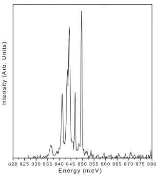
To study the emission from small numbers of InAs/InP quantum dots grown at the apex of rectangular based pyramidal templates such as those shown in Figure 7 we µ-PL techniques. In this way, luminescence emission from single pyramid structures can be obtained. The emission of such structures changes character substantially from pyramid to pyramid because of changes in the number and coupling of quantum dots. Different pyramids display different numbers of sharp emission lines with energies ranging between approximately 1100meV and 750meV depending upon the template dimensions and the amount of InAs deposited. An example of emission from a square based pyramid with a 1µm base dimension is shown in figure 9. The emission consists of a manifold of peaks centred around 845meV with a spectral width of approximately 400µeV, determined by the spectral resolution of the data acquisition system. Such an emission characteristic may represent the output from a complex Figur e 8. Low temper atur e photoluminescence spectr a obtained fr om str ipe geometr y InAs/InP nanotemplates of var ying width. Dot and wetting layer (WL) emission is obser ved fr om mater ial on both the (001) and (110) sur faces. Spectr a ar e labeled with the width of the oxide window used in the gr owth.
quantum dot molecule or the emission from a single quantum dot with spatially separated electron and hole wavefunctions, as observed previously for InP/InGaP quantum dots.
Fig. 9 Low temper atur e photoluminescence spectr um fr om a single, 1mm base, InAs/InP nanotemplate pyr amid
GaAs-Based Structures
2.5 Selective Gr owth of Quantum Dot Ar r ays on Patter ned Substr ates
Selective QD growth on GaAs substrates has been achieved using an alternative technique. By adding a strain layer in predefined regions, we can control the formation of QDs below the critical thickness at any given region. Single dot formation has been achieved on small e-beam defined mesas. We have also achieved two-dimensional arrays of single QDs using this technique.
The procedure for such growth is shown in Fig.10. A thin InGaAs layer together with a GaAs cap layer are first deposited on a GaAs substrate. Because of the lattice mismatch, the InGaAs layer is strained. Small mesas are then defined by e-beam lithography and chemical etching. The sample is put back in the MBE system for the growth of InAs quantum dots. Usually the amount of InAs layer deposited has to exceed a certain critical thickness to accumulate enough strain before the quantum dots are formed. But, since the mesas are prestrained, a less
amount of InAs layer is needed to form the quantum dots on the mesa top. On the GaAs surface where the InGaAs layer has been etched away, no quantum dots are formed because the InAs deposited is too thin to have enough strain for dot formation. If the mesa size is small enough, only one quantum dot can form on the top.
Figur e 10. Flow diagr am of selective gr owth of single QDs. Sequentially fr om top to bottom, str ain sour ce pr epar ation, e-beam patter ning, and MBE r e-gr owth.
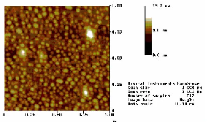
Fig.11 shows the AFM image of a two-dimensional quantum dot array grown with this technique. Each mesa top has only one quantum dot.
This technique of selectively placing single QDs should find application in many new generation quantum devices such as in single electron transistors, distributed feed-back lasers, and single-photon photodetectors.
Figur e 11. AFM image of a two-dimensional single quantum dot ar r ay 8 2 0 8 2 5 8 3 0 8 3 5 8 4 0 8 4 5 8 5 0 8 5 5 8 6 0 8 6 5 8 7 0 8 7 5 8 8 0 In te n s it y ( A rb . U n it s ) E n e rg y (m e V )
2.6 Self-Assembled Quantum Anti-Dot Gr owth
Quantum anti-dot is another form of quantum structure. The potential in the dot region is higher instead of lower than the outside region. Many interesting phenomena can be expected from such structure. But the growth of anti-dots has not been carefully studied in the past. In this project, we did a systematic study on the growth of GaAs quantum anti-dots in InAs matrix. The growth is still based on strain-induced self-organization.
The samples were grown on a (100) InAs substrate by a solid-source MBE system equipped with an arsenic cracker cell. After native oxide desorption at 510oC, a 0.5µm InAs buffer layer was deposited before the GaAs growth. With about 40nm InAs spacer, 1.5ML, 1.75ML, 2ML, 2.25ML, and 2.5ML GaAs were deposited sequentially. Migration-enhanced epitaxy (MEE) method was used for each GaAs layer growth. That is, after each 0.25ML GaAs deposition, we introduced growth interruption for 10 seconds. In this 10 seconds period, the arsenic shutter was kept open for the first 5 seconds, and then closed for the next 5 seconds. The growth temperature and the growth rate for GaAs were 500oC and 0.1µm/hr, respectively. The III/V beam equivalent pressure ratio of In (Ga) was 25 (10).
Fig.12 shows an atomic force microscope (AFM) image of the grown sample. From the image, a clear 3-D, dot-like morphology is observed. From the surface profile analysis of the AFM, the shape of the islands is almost isotropic, with about 15-35nm in base diameter and about 2-4nm in height. The density of the GaAs antidots was about 3-4x1010cm-2 averaged over several observed 1x1µm2 images.
Figur e 12. AFM image of GaAs anti-dots on an InAs substr ate.
Fig.13 shows the transmission electron microscopy (TEM) images for the sample. There are 5 layers of GaAs with different thickness as stated above. But in this case, a thick InAs capping layer was grown above the last GaAs layer. From the figure, we can see that for less than or equal to 2.25ML GaAs deposition, there is no 3-D island formation. For the 4th layer (with 2.25ML GaAs) from the bottom, strain fields in some isolated spots were observed.
In the layer with 2.5ML GaAs deposition, clear quantum anti-dots were observed. The high-resolution TEM image for one of the GaAs antidots formed on the sample surface is also shown in the figure. From the figure, the exact size of the GaAs antidot could be obtained. The base diameter and height are about 20nm and 2.5nm, respectively. It is consistent with the AFM observation.
From our study, we can conclude that the critical thickness of 2-D to 3-D morphology transition for GaAs antodots on InAs is between 2.25ML and 2.5ML. It is considerably larger than 1.5ML, the critical thickness for InAs QD formation on GaAs.
Figur e 13. TEM image of the GaAs quantum anti-dots in InAs matr ix
2.7 Resonant Tunneling thr ough Quantum Dots Resonant tunneling is one of the most fundamental quantum phenomena to be observed in any quantum structure. It is important to both fundamental physics and nano-device applications. However, the ground state energy of InAs QDs in GaAs or even AlAs matrix are usually lower than the Fermi level in the GaAs emitters in a resonant tunneling structure, making it difficult to tunnel through the states of InAs QDs. The reported results vary from device to device and suffer from the reproducibility problem. In this work, we replace the GaAs emitters with InGaAs quantum wells. From the results of photoluminescence (PL) and current-voltage (I-V) characteristics, we can obtain unambiguously the resonant tunneling through the InAs QDs, both controllably and reproducibly.
Fig.14 shows the resonant tunneling structure used in the study. InGaAs quantum wells were used as the
emitter and the collector. In this way the quantized energy level can easily align with the quantum dot state in the middle to facilitate resonant tunneling.
Figur e 14. Str uctur e of the quantum dot r esonant tunneling str uctur e.
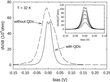
The measured differential resistance versus voltage curve for the above structure is shown in Fig.15. The curve of a structure with no InGaAs emitter is also shown for comparison. It is clear that with an InGaAs emitter, there is a dip in the differential resistance near V = 0, indicating resonant tunneling through quantum dots. The
structure without the InGaAs emitter does not the dip in the curve. This characteristic is observed on all the devices. The inset shows the curves measured on five different devices. Each one of them shows the dip in its differential resistance curve. So the resonant tunneling phenomenon is unambiguously observed.
Figur e 15. Differ ential r esistance vs. voltage cur ve for r esonant tunneling thr ough quantum dots.
2.8 Spin-Dependent Scatter ing
The electron’s spin-orbit interaction can cause many spin-sensitive phenomena in some of the semiconductors. With the potential applications of spintronics, filtering out electrons with certain spin polarization is very important. We have studied the effect of spin-orbit interaction on electron scattering by semiconductor quantum dots and quantum anti-dots in two-dimension and three-dimension systems. We found that measurable angular dependent spin polarization can be obtained. Partial wave method was used to calculate the scattering differential cross section.
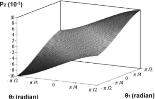
Figur e 16. Spin polar ization after scatter ed by a GaAs/InAs anti-dot.
Fig.16 shows the calculated spin-polarization as a function of the scattering angle and the electron energy for
a scattering by a quantum anti-dot in a two-dimension system. The polarization is defined as the ratio between the difference in differential cross section (for different spins) and the average cross section. Very clear left and T = 32 K bias (V) -0.15 -0.10 -0.05 0.00 0.05 0.10 0.15 0.20 0.25 d V/ d I (1 0 6 o h m ) 0 20 40 60 80 without QDs with QDs bias (V) -0.10 -0.05 0.00 0.05 0.10 dV /dI( 10 6ohm ) 0 20 40 60 80 100 120 InGaAs E0 InAs QDs
right asymmetry is observed. With such phenomenon, it is possible to separate electrons with different spin polarizations. If a spin-polarized electron beam enters the sample, anomalous Hall effect will be observed even without magnetic field. It should be mentioned that an anti-dot is much more effective in producing spin-dependent scattering than a quantum dot. The polarization vector caused by the scattering from a dot is opposite to that from an antidot. The effect is several times stronger in
a two-dimensional channel than in a three dimensional medium.
Figur e 17. The geometr y of the double scatter ing event. We have also studied the effect of double scattering on the spin polarization. Dependent on the relative location of the second scattering center, the effect on the spin filtering can be enhanced.
Fig. 17 shows the geometry of the double scattering and the relative locations of the scattering centers. After the first scattering, the initially unpolarized beam becomes partially polarized and then hits the second scatterer. The final spin polarization is calculated as a function of θ1
andθ2, which is the scattering angle for the two scattering
events. Fig. 18 shows the polarization as a function of the scattering angleθ1 and the electron’s energy after the first
scattering. Fig.19 shows the calculated result for a double scattering from two anti-dots. Clearly, the spin polarization is enhanced by the double scattering. The maximum polarization achieved after the second scattering is twice that of the polarization after the first scattering.
Figur e 18. Spin polar ization as a function of scatter ing angle and electr on ener gy after fir st scatter ing
Figur e 19. Spin polar ization as a function of scatter ing angles after double scatter ing.
3 SUMMARY AND REMARKS
Under the support of NSC-NRC collaboration program, we have performed research in semiconductor quantum dots, and the ability to position those dots, and quantum anti-dots. Some of the highlights of the achieved results are presented here. When we started the program three years ago, nanotechnology was just at the infant stage, since then both countries have started national efforts in this area. During this time there have been visits between the scientific staff from both countries, and now both laboratories are actively involved in the nanodevice research. We are happy that we could be in the forefront of this activity and our program was one of the first chosen for the NSC-NRC collaboration. The results obtained in this program have undoubtly made contributions to the nanoscience and technology. This work has resulted in more than 8 publications (NRC), and the involvement and training of 2 personnel (NRC). Our research will continue and we hope that we can collaborate again in the future.
![Figur e 2. Plan-view, br ight-field TEM images of InAs/InP quantum dots viewed down the [001] zone axis displaying the evolution of quantum dots with gr owth inter r upt time](https://thumb-ap.123doks.com/thumbv2/9libinfo/8267910.172559/2.893.86.429.588.713/figur-field-images-quantum-viewed-displaying-evolution-quantum.webp)