國 立 交 通 大 學
電子工程學系 電子研究所 碩士班
碩
士
論
文
對染料敏化太陽能電池之結構調整與相應電子行為分析
Study of Electron Behaviors in Structure Modified Dye Sensitized Solar Cells
研 究 生:郭宇彥
指導教授:簡昭欣 教授
對染料敏化太陽能電池之結構調整與相應電子行為分析
Study of Electron Behaviors in Structure Modified Dye Sensitized Solar Cells
研 究 生:郭宇彥 Student:Yu -Yen Kuo
指導教授:簡昭欣 Advisor:Chao-Hsin Chien
國 立 交 通 大 學
電 子 工 程 學 系 電 子 研 究 所 碩士班
碩 士 論 文
A Thesis
Submitted to Department of Electronics Engineering & Institute of Electronics College of Electrical Engineering and Computer Science
National Chiao Tung University in partial Fulfillment of the Requirements
for the Degree of Master
in
Electronics Engineering
July 2007
Hsinchu, Taiwan, Republic of China
i
對染料敏化太陽能電池之結構調整與相應電子行為分析
學生:郭宇彥
指導教授
:簡昭欣 教授
國立交通大學 電子工程學系電子研究所 碩士班
摘
要
為了使染料敏化太陽能電池成為更有效率的太陽能轉換元件,元件效率
與穩定性的進一步提升是當前極重要的課題,於本論文中,完成三種相異
結構的染料敏化太陽能電池並對各別元件的基本光電特性與電子行為進行
量測觀察與分析比較。
首先,針對一般染料敏化太陽能電池元件的特性進行分析,透過改變元
件製作的條件,了解相應的光電特性表徵並對目前已發展的量測方法與元
件工作理論進行回顧。
接著根據過往文獻記載的實驗結果,在元件製作中使用四氯化鈦溶液對
二氧化鈦奈米結晶粒工作電極表面進行處理;相較於未處理的元件,經過
四氯化鈦處理的元件於光電特性上有十分顯著的增益。透過電子行為的量
測並與基本元件實驗結果相較,可了解四氯化鈦所造成的增益主要是彰顯
在電子電洞復合速率的抑制上,而在電子傳輸的速率上並無造成顯著地影
響;再進一步從表面能態密度的量測結果可得知復合速率的抑制應與表面
能態密度的減低有關。
由於電子有效擴散長度的有限性,期望能透過再進一步改善染料敏化太
ii
陽能電池的吸收特性以減少有效吸收層的厚度並同時降低元件的材料消
耗,因此在基本元件中引入了具不同粒徑的二氧化鈦結晶粒作為光散射
層,於本論文中對散射層製作條件進行討論;而在引入所製成均勻分佈的
散射層後,於較薄吸收層的元件中確實觀測到所造成的增益,同時以進一
步的光電特性結果佐證此一增益確實與期望相符,即散射層所造成。
為使電子傳輸速率能有進一步提升,本論文之第三部分透過引入陽極氧
化製成之二氧化鈦奈米管狀結構完成染料敏化太陽能電池,首先針對陽極
氧化條件對奈米管之影響進行探討,而完成的元件與傳統奈米晶粒之元件
相較,於元件的特性上觀測到許多不同的結果,是接下來值得進一步研究
的方向,最後對於不同條件所完成的元件所表現的特性於本論文中進行了
一點初步的討論,亦提供奈米管元件接下來發展方向的一些參考。
於本論文中,完成了三種不同結構的染料敏化太陽能電池,並透過進階
的光電特性量測方法對於結構變化所造成在電子行為上的影響進行解釋與
推測,在染料敏化電池元件的發展過程中能夠提供良好的參考方向,相信
一個更加理想的太陽能元件是能夠被完成與使用的。
iii
Study of Electron Behaviors in Structure Modified Dye Sensitized Solar Cells
student:
Yu-Yen KuoAdvisors:Dr.
Chao-Hsin ChienDepartment of Electronics Engineering & Institute of Electronics
National Chiao Tung University
ABSTRACT
To improve the energy transfer efficiency of dye sensitized solar cell furthermore and thus lead to more convenient usage of solar energy, complete knowledge of DSSC at present stage is necessary. In this dissertation, DSSC with three different structures were fabricated and the behaviors of electrons for each were analyzed through developed photo-electrical methods.
In the start, basic properties of normal DSSC were examined and characterized. Developed theories about the working principle of DSSC, light absorption, electron injection and transportation, and the basics of measurement methods for analyzing electrons behavior were reviewed separately.
With a preliminary understanding of conventional DSSC, the well known efficiency
enhancement method, the passivation of TiO2 by titanium tetrachloride, was applied; the
photo-electrical improvements were obviously observed from experimental results. To discover the cause of the enhancements, the electrons behaviors were measured. The recombination of electrons was inhibited when compared with non-passivated devices (near one ordered difference in the time constants) while the diffusion remains almost the same. It was thought that the inhibition of recombination be mainly due to the variation of surface states according to DOS measurement results.
Because of the limitation on the diffusion length, it is preferred to achieve better absorption in thinner layer; then, a light scattering structure was applied to conventional
iv
DSSC by different sized nano-crystal. The conditions of the fabrication of scattering layer were tested and an optimized process was achieved to derive a uniform morphology of the scattering layer. With the application of the scattering layer, the enhancement of absorption was observed and the photo-voltage is enhanced in thinner layered devices.
Based on observed experimental results, it was thought that the preliminary limiting factor for DSSCs at present stage be the low electron collection efficiency due to the low diffusivity in nano-crystallite film. To accelerate electron transportation, ordered nano-tube structure was fabricated and applied to DSSC successfully. Basic characterizations were done and some improvements were obtained while some disadvantages were expected to be overcome with advanced modifications in research afterward.
In this dissertation, DSSCs with three different structures (conventional, scattering layer applied, and nano-tube applied) were fabricated and characterized. Different photo-electrical behaviors were observed in these devices due to the different nature of structural issues.
v
誌
謝
在兩年的實驗過程中,因為有許多人的協助,方得以順利完成到目前為止的研究, 謝謝你們。明瑞學長、志彥學長、兆欽學長、家豪學長、阿國學長等各位實驗室的學長, 謝謝你們在實驗初始時的引領與各項儀器使用上的訓練;欣哲、効諭、敬倫、宣凱、弘 森、猛飛各位同學,謝謝你們在平日的幫助和實驗過程中的支援與討論,謝謝。 奈米中心的陳悅婷小姐、林聖欽先生、陳明麗小姐和 NDL 的劉育彬學長、簡依玲小 姐、郭美玲小姐、賴明志先生,謝謝你們在儀器使用上的幫助,使實驗的進展能夠順利; 黃文賢學長,謝謝您的幫忙,因而能有良好的實驗環境並且在化學品使用過程上不致有 不方便的情況。張簡鵬崇學長、李美儀學姐,十分謝謝你們在電化學實驗上的協助與討 論,讓主要的實驗量測部分能很快、很順利的完成。 特別要感謝我的指導老師,簡昭欣老師,謝謝您在研究中、生活上所給予的支持, 並且提供我們十分良好的研究環境,使我能專心在自己的研究上,真的很謝謝您。 最後,要謝謝我的家人一直以來在我求學、研究過程中的照顧和支持。我相信在接 下來的時間裡,能夠實現目前的理想。希望各位健康、平安、生活自在。
vi
Contents
Abstract (Chinese)………... i
Abstract (English)……… iii
Acknowledgement……… v
Contents……… vi
Table Captions………. vii
Figure Captions……….viii
1. Introduction……….. 1
References……….………..……….. 7
2. Experimental Methods………. 8
2.1 Materials and equipments used in fabrication ………. 8
2.2 Characterization of materials……….. 9
2.3 Photo-electrical measurements……….. 10
2.3.1 Current-voltage (I-V) measurement……….. 10
2.3.2 Electrical impedance spectroscopy (EIS) ………. 13
2.3.3 Photovoltage transient ……….. 13
2.3.4 Photocurrent transient………. 15
2.3.5 DOS measurement……… 16
References……….………..……….. 18
3. Dye Sensitized Solar Cell……… 19
3.1 DSSC –working mechanisms……… 19
3.1.1 Absorption of light……….. 19
3.1.2 Electron injection ……… 23
3.1.3 Electron transport in TiO2 ……….. 26
3.1.4 Hole transport in ionic electrolyte….………. 28
3.1.5 Charge recombination mechanisms……….. 29
3.2 Fabrication process……….. 30
3.3 Photo-electrical analysis……….. 32
References……….………..……….. 51
4. Scattering Layer Applied DSSC……….. 53
4.1 Fabrication process……….. 54
4.2 Properties of the scattering layer ……… 55
4.3 Photo-electrical analysis……….. 58
References……….………..……….. 67
5. Nano-tube Applied DSSC………. 68
5.1 Fabrication process……….. 69
5.2 Properties of TiO2 nano-tube ……… 71
5.3 Photo-electrical analysis……… 79
References……….………..……….. 85
6. Summary and Outlook……… 86
vii
Table Captions
Table 1.1 energy payback time of different type solar cells p.5
Table 3.1.1 parameters and corresponding values used in DFT calculations p.23
viii
Figure Captions
1. Introduction
Fig.1.1 basic structure of DSSC p.5
Fig.1.2 primary electron transfer paths in DSSC p.5
Fig.1.3 solar spectrum at different level p.6
2. Experimental Methods
Fig.2.3.1 setup of I-V and EIS systems p.11
Fig.2.3.2 consistency in photocurrent in repeated measurements p.12
Fig.2.3.3 current lowering cue to use of mask in measurement p.12
Fig.2.3.4 photovoltage/photocurrent transient system p.14
Fig.2.3.5 pulse generation limit of the solid switch circuit p.15
Fig.2.3.6 consistency in 10us transient response of the amplifier circuit p.15
Fig.2.3.7 combined DOS system p.17
Fig.2.3.8 the basic concept of DOS measurement p.17
3. Dye Sensitized Solar Cell
Fig.3.1.1 transmission spectrum of FTO substrate used in the experiment p.20
Fig.3.1.2 (a) the main peaks of the absorption of N719 dye and p.21
(b) the chemical structure of N3 andN719
Fig.3.1.3 calculated eigenstates of N3 dye p.22
(a)LUMO (b)HOMO (c)LUMO +1
(d)HOMO-1 (e)LUMO+2 (f)HOMO-2
Fig.3.1.4 chemical structure of N3 dye in the calculation p.23
Fig.3.1.5 selected eigenstates of N3 dye adsorbed on TiO2 anatase (101) surface
Occupied : (a)435 (b)436 (c)437
Vacant : (d)444 (e)446 (f)448 p.25
Fig.3.1.6 calculated eigenenergies of N3 dye adsorbed on TiO2 anatase(101) p.26
Fig.3.1.7 SEM image of fabricated TiO2 nanocrystal layer p.27
Fig.3.2.1 (a) fabrication flow of dye sensitized solar cells p.30
(b) the picture of completed DSSC device
Fig.3.2.2 the two nancrystalline layers with different porosity and thus different
ix
Fig.3.3.1 (a) darkcurrent and (b) photocurrent to voltage characteristics of DSSC
fabricated on different substrates
(1) ITO 30 Ω / □ (2) FTO 15 Ω / □ (3) ITO(2) 100 Ω / □ p.39
Fig.3.3.2 EIS of DSSC with different substrate p.39
(1) ITO 30 Ω / □ (2) FTO 15 Ω / □ (3) ITO(2) 100 Ω / □
Fig.3.3.3 (a) darkcurrent and (b) photocurrent to voltage characteristics of DSSC fabricated by different paste solvent
(1) alpha-terpineol and (2) poly ethylene glycol p.40
Fig.3.3.4 EIS of DSSC by different paste solvent p.40
(1) alpha-terpineol and (2) poly ethylene glycol
Fig.3.3.5 (a) dark current and photocurrent to voltage characteristics, (b) EIS, and (c) EIS phase plot of DSSCs using different electrolytic solvent
(1) PC propylene carbonate and (2)MPN methoxypropionitrile. p.41
Fig.3.3.6 (a) current to voltage characteristic under different light intensities
(b) EIS plot at 100mW/cm2 and 50mW/cm2 and p.42
(c) EIS phase at 100mW/cm2 and 50mW/cm2
Fig.3.3.7 photocurrent and dark current to voltage properties of DSSC of highly
transparent bottom layer with p.43
(1) TiCl4 treated 5um, (2)TiCl4 treated 4.5um, and (3)non-treated 5um
Fig.3.3.8 (a) relaxation behaviors and (b)extracted recombination constants of
DSSCs of p.44
(1)TiCl4 treated (2)non-treated
Fig.3.3.9 dark current and photocurrent to voltage properties of DSSC (1)with TiCl4
and (2)without TiCl4 treatment on lower transparency bottom layers p.45
Fig.3.3.10 (a) current transient with and without TiCl4 treatment and (b) (c) fitted by
single exponential function p.46
Fig.3.3.11 photocurrent transient of TiCl4 treated DSSC at varied background
intensities p.49
(a)(b) the relative background levels
(c)(d)(e)(f)(g)(h) single exponential fitted results (i) extracted diffusion time constants
x
Fig.3.3.12 Extracted surface DOS versus energy levels of DSSC of p.50
(1) TiCl4 treated
(2) non-treated
4. Scattering Layer Applied DSSC
Fig.4.1 (a) the SEM image of 100nm scattering particles used in the experiment
(b) the transmission spectrum of film composed of P25 and 100nm
particles p.53
Fig.4.1.1 the fabrication flow of scattering layer applied DSSC p.54
Fig.4.1.2 the photographs of scattering applied DSSC taken from p.54
(a) scattering layer side
(b) bottom layer side after dyeing
Fig.4.2.1 the morphologies of scattering layer after different heat processes p.57
(a)450°C (b)300°C
(c)450°C on P25
(d) 270°C on P25 then 450°C
(e) comparison of the scattering layer and the bottom layer (f)270°C
Fig.4.3.1 The photocurrent and dark current to voltage characteristics of two kinds of devices with highly transparent bottom layer:
(1) P25 layer and (2) P25 layer with scattering layer, the illumination
intensity is 100mW/cm2 . p.61
Fig.4.3.2 The (a) EIS and (b) phase plot of two kinds of devices with highly
transparent bottom layer: p.62
(1) P25 layer and (2) P25 layer with scattering layer under illumination
intensity 100mW/cm2 and open circuit voltages.
Fig.4.3.3 The photocurrent and dark current to voltage characteristics of two kinds
of devices with normally transparent bottom layer: p.63
(1) P25 layer and (2) P25 layer with scattering layer, the illumination
intensity is 100mW/cm2 .
Fig.4.3.4 The (a) EIS and (b) phase plot of two kinds of devices with normally
transparent bottom layer: p.64
xi
intensity 100mW/cm2 and open circuit voltages.
Fig.4.3.5 The (a) photovoltage transient behaviors and (b) extracted recombination
time constants versus photovoltage of devices with (1) P25(TiCl4 treated)
and (2) P25(TiCl4 treated) + scattering layer p.65
Fig.4.3.6 the photocurrent transient behaviors of three different devices p.66
(1) P25(TiCl4 treated),
(2) P25(TiCl4 treated)+scattering layer, and
(3)P25 + scattering layer.
5. Nno-tube Applied DSSC
Fig.5.1 (a ) the modified device structure of nanotube applied DSSC and p.69
(b) the morphology of fabricated tube array.
Fig.5.1.1 the fabrication flow of nanotube based DSSC (the image of the completed
device is also inserted) p.69
Fig.5.1.2 the oxidation current at the initial stage p.70
Fig.5.2.1 the different stages of the formation of the tube structure at constant
voltage (a) metal surface oxidized, (b) small pores formed on the oxide, (c) the small pores are deepen by the enhanced etch rate, (d) voids in the region between pores are formed, (e) both the pores and voids are stably
deepen, and thus tube structure can be produced. p.73
Fig.5.2.2 The small pores formed on the oxide initially p.73
Fig.5.2.3 Images of TiO2 tube anodized under different potentials (a)15V (b)20V
(c)30V (d)40V (e)50V p.76
Fig.5.2.4 The dependence between tube diameter and oxidization potential p.76
Fig. 5.2.5 The tube lengths described in the article are all determined by SEM images, tubes fabricated at 40V with different periods result in (a) 1μm
and (b )5μm. p.77
Fig.5.2.6 The crystalline characteristics are changed with applied crystallization
conditions (a) as deposited, amorphous, (b) 400˚ C 5hrs, anatase signal occurs, (c)450˚ C 5hrs, anatase signal stronger, (d) the crystalline
properties are different from the nanocrystal case, where both anatase and
rutile signals were observed. p.78
xii
of devices composed of nanotube with the same diameters but different tube lengths (1) 1um at 40V applied potential and (2) 5um at 40V applied
potential, the illumination intensity is 100mW/cm2 . p.81
Fig.5.3.2 The EIS results of nanotube DSSCs of (1)40V 1um and (2)40V 5um (a) the Nyquist plot, the impedance value are changed and (b) the primary difference is on certain frequency and (c) the variation on the frequency is thought to be a simultaneous change on two interfaces compared with
nanocrystalline cases. p.82
Fig.5.3.3 the recombination time constants of nanotube case are very different to
nanocrystalline ones. The difference is near two orders. p.83
Fig.5.3.4 photocurrent transient behaviors of nanotube DSSC is slower, when compared to nanocrystalline cases; it is an unwanted results, and
discovery of the reason and improvement is necessary. p.83
Fig.5.3.5 The photocurrent and dark current to voltage characteristics of two kinds of devices composed of nanotube with different diameters but the same tube lengths (1) 1um at 20V applied potential and (2) 1um at 40V applied
1
Introduction
1. Introduction
The demand of energy nowadays grows up very rapidly. Nearly all modern technologies consume energy. Although the connection between energy and one’s life is so tight, the methods that human derives energy are not efficient and smart enough thus large amount of pollutions are produced in the derivation and transformation of usable energy. As an example, one of the major methods used to drive motors is the direct burning of fossil fuel, in which air pollutants as carbon oxide, carbon dioxide, and sulfuric oxide are produced. While the accumulation of pollutant causes severe problems to the environment, technology for energy production in a more efficient way and environment benign is necessary.
One of the possible technologies for renewable energy is the solar cell, which is a device that converts energy of sunlight to electricity directly. It is certain that the resource, energy from the sun, is sufficient for human use since the average power that sunlight converts to earth is 86PW while the power consumption of human activities is 15TW [1].
The working principle of the conventional solar cell is based on the properties of a p-n junction structure. Incident photons interact with electrons in the semiconductor bulk and cause the electrons be excited to the conduction band. The build-in potential in the depletion region of the p-n junction causes separation of electrons in the conduction band and holes in the valence band. When electrons and holes are separated and drifted out of depletion region, each one will transport to corresponding electrode by diffusion because of the concentration gradient induced in the bulk material. Briefly speaking, the operation of a solar cell includes three major stages, absorption separation and transportation.
The technology of solar cells could be separated to three generations; the first one consists of the structure using single or poly crystalline substrate, could be Si or III-V material,
2
Introduction
usually with device thickness over 300um for efficient light absorption ability. Because of the sufficient light absorption and high diffusivity of both electrons and holes in these single crystalline materials, higher conversion efficiency could be obtained in these devices. For the nature of indirect band-gap of silicon based device, sub-band-gap absorption is less efficient than III-V epitaxial type and the conversion efficiencies are 24% for silicon single crystalline cells and 40% for GaAs based multi-junction cells [2].
For terrestrial applications of solar energy, the 2nd generation thin film devices were
developed to lower the high cost of 1st generation devices, mainly from the consumption of
material. Due to the insufficient absorption of light but shorter transport path of the thin film, light scattering structure are usually applied and different materials beside poly-Si, amorphous Si like II-VI (CdSe, CdTe) and quaternary (CIGS) compounds are used [3]. Considering all
the issues, the payback time of the 2nd generation devices is superior to the 1st ones. But even
the 2nd generation devices, it seems that transforming solar energy is still not efficient enough.
New solar cells with higher efficiency but lower price are necessary for the convenience of solar energy use.
Taking an examination of both 1st and 2nd generation devices, one might see that both are
based on the same operation principle, i.e. electron hole pairs produced when the bulk material absorbs sunlight, then separation of electron hole pairs is enhanced by the built in voltage due to the p-n junction and separated carriers diffuse to opposite electrodes. Based on the conventional semiconductor physics, there is a limit for this process, the Shockley limit, which is specified depending on the band-gap of material of the device, and the Shockley limit is always lower than the thermodynamic limit of the energy transformation from solar energy to electricity [4].
For the 3rd generation device, new methods are expected to be designed to achieve the
goal. One possible method is based on the photo-electrochemical solar cell, also named as dye sensitized solar cell.
3
Introduction Dye sensitized solar cell, proposed by M.Grätzel at 1991 [5], works different from conventional structures; the operation of this device is based on the catalytic properties of wide band gap metal oxide and is similar to mechanism of photosynthesis on a certain level.
The basic structure of the device is shown as Fig.1.1, the specially designed dye molecule, as the major light absorber, are on one side chemically adsorbed on the surface of titanium dioxide deposited on TCO (transparent conducting oxide) glass substrate while the
other side is immersed in I- / I3- electrolyte with catalytic Pt or carbon layer as the counter
electrode.
The light harvesting process of DSSC is depicted in Fig.1.2 and each step is described as follows:
(1) The device is illuminated from TCO side. The electron at the ground state of the
dye is excited to the different excited states depending on the energy of absorbed photon.
(2) An ultra fast electron injection from excited state of dye molecule to the
conduction band of TiO2 happens mainly due to Metal to Ligand Charge
Transfer (MLCT) [6].
(3) The injected electrons will diffuse to TCO side due to concentration gradient of
electrons in the conduction band of TiO2 and at the same time
(4) the left hole in the ground state of dye will be reduced by I- / I3- ionic electrolyte
through the reaction process as:
3I-+ 2h+(Dye) I3
-and I3
+ 2e- (Pt) 3I- at the counter electrode
As shown in the Fig.1.2, when DSSC is illuminated, most of the sunlight could be
4
Introduction
of wavelength of visible light, which is the major component of solar spectrum (Fig.1.3). The most difference between DSSC and conventional solar cells is that the absorption and charge separation processes are accomplished on the dye molecule and the interface of
dye/TiO2. Due to the operating principle of DSSC, abundant adsorption of dye molecule is
necessary to achieve sufficient absorption of incident sunlight. For this reason, the titanium
dioxide film applied in DSSC for dye adsorption is composed of TiO2 nano-crystalline with
diameter that is about 20nm.
Dye sensitized solar cell have many special properties comparing with conventional solar cells and many are more advantageous as being used as a photovoltaic device. First of all, the angular dependence of incident sunlight is uniform since the difference in absorption of dye molecule for light from different direction is not obvious and the large amount of adsorbed dye cause the orientation effect much less. When it is used for sunlight harvesting, the incident angle varies a lot in a day and it is important for the uniformity of light absorption thus no additional angle trace equipment is necessary. Table.1.1 [7, 8] are lists of the energy payback time of different solar cells; it is obvious that the payback time for DSSC is much shorter when compared with other ones since the demand of the purity of materials used in DSSC is less than conventional semiconductor devices, so even with a little lower efficiency now, the total payback time is still shorter, that means it could be a better device for solar energy transformation.
5
Introduction
Cell Technology Energy Payback Time (EPBT) (yr)
Single-crystal silicon 2.7
Non-ribbon multicrystalline silicon 2.2
Ribbon multicrystalline silicon 1.7
Cadmium telluride 1.0
Dye sensitized solar cell [8] 0.8
Fig.1.1 basic structure of DSSC
Fig.1.2 primary electron transfer paths in DSSC Table 1.1 energy payback time of different type solar cells
6
Introduction
ASTM G173-03 Reference Spectra
0.00 0.25 0.50 0.75 1.00 1.25 1.50 1.75 2.00 250 500 750 1000 1250 1500 1750 2000 2250 2500 2750 3000 3250 3500 3750 4000 Wavelength nm Sp e c tr a l Ir ra d ia n c e W m -2 n m -1 Etr W*m-2*nm-1 Global tilt W*m-2*nm-1 Direct+circumsolar W*m-2*nm-1
7
Introduction
References
[1] BP Statistical Review of World Energy, June 2008.
[2] R. R. King; D. C. Law; K. M. Edmondson; C. M. Fetzer; G. S. Kinsey; H. Yoon; R. A. Sherif; N. H. Karam, Appl. Phys. Lett. 2007, 90, 183516.
[3] Jef Poortmans; Vladimir Arkhipov. Chichester, Thin film solar cells: fabrication,
characterization and applications, West Sussex, England, Wiley, c2006.
[4] Seraphin, B. O. ed, Solar energy conversion: solid-state physics aspects; Berlin, Springer-Verlag, 1979.
[5] B. O’Reagen; M. Gratzel, Nature 1991, 353, 6346. [6] A. Hagfeldtt; M. Gratzel, Chem, Rev. 1995, 95, 49.
[7] V. Fthenakis; E. Alsema, Progress in Photovoltaics, 2006, 14, 3, 275.
[8] M.J. de Wild-Scholten; A.C. Veltkamp, Environmental Life Cycle Analysis of Dye
Sensitized Solar Devices; Status and Outlook; ECN Solar Energy.
[9] Air Mass 1.5: ASTM E-891 and ASTM E-892, both combined into ASTM G-159; NREL.
8
Experimental Methods
2. Experimental Methods
2.1 Materials and equipments used in experiment
Used materials and chemicalsSubstrate
type thickness sheet resistance
Glass / ITO 0.7mm 100 Ω / □
Glass / ITO 0.7mm 30 Ω / □
Glass / FTO 4mm 15 Ω / □
Glass / FTO 1mm 10 Ω / □
Ti foil 250um STREM CHEMICALS
TiO2 nano-crystalline powder
TiO2 P25 Degussa TiO2 anatase 98% ACROS ORGANICS Dye N719 cis-bis(isothiocyanato)- Solaronix bis(2,2'-bipyridyl-4,4'-dicarboxylato) -ruthenium(II) bis-tetrabutylammonium
Ingredient of TiO2 paste
alpha terpineol SHOWA
ethyl cellulose SHOWA
poly ethylene glycol M.W. 20000 SHOWA
Ionic electrolyte
iodine TCI
lithium iodide ACROS ORGANICS
potassium iodide SHOWA
4-tert-butylpyridine ACROS ORGANICS
3-methoxypropionitrile ACROS ORGANICS
9
Experimental Methods Anodic Oxidization
ammonium fluoride SHOWA
sulfuric acid SHOWA
ethylene glycol Scharlau
Others
titanium tetrachloride SHOWA
Equipments in device fabrication
Atmospheric Anneal Furnace (KH Union Co., Ltd)
Sputtering System (Ion Tech Microvac 450CB)
E-gun Coater (VTI E/B GUN COATER)
2.2 Equipments for characterization of materials
Surface Profiler (Dektak 3030)
UV-Visible Spectrometer (UV-2501PC SHIMADZU)
Scanning Electron Microscope (Hitachi S-4000)
High-Resolution Scanning Electron Microscope
& Energy Dispersive Spectrometer (Hitachi S-4700I) Focused Ion Beam
& Electron Beam System (FEI Nova 200)
10
Experimental Methods
2.3 Photo-electrical measurements
All the measurement systems were self-built. The specifications for the setup are described in the following paragraphs.
2.3.1 Current-voltage (I-V) measurement
Figure 2.3.1 shows the apparatus for the basic I-V measurement, which included two parts—the light source and the electrical measuring system. Newport Oriel 96000 150W Xe lamp and AM1.5G filter 81094 were used as the solar simulator; the optical power of incident light was measured by the thermopile detector 818P-010-12 and
calibrated to 100mW/cm2 before measuring. For characterizing the I-V properties, the
electrochemical potentiostat / galvanostat EG&G model 273A was connected to the device in two probing modes; conventional solar cells were tested to identify the validity of the measuring system and the results were consistent with I-V characteristics from other equipments.
For the measurement of solar cell I-V characteristic, specific mask with defined transparent area was used so that the effective area among each measurement could be kept being constant. In this experiment, since the active area was defined during processing, no additional mask was necessary in the photo-electrical measurements. The I-V characteristics with/without mask applied are shown in Fig.2.3.2 and the
difference in these two curves was in the Isc region, which is similar to the result in
Ref.1. We, thus, thought the lowering of photocurrent is mainly due to the edge shading effect caused by the presence of mask. It seems that the I-V characteristics were not changed no matter the mask was employed or not. As a result, in the experiment all the measurements have been done without mask.
11
Experimental Methods It should be mentioned that all the photoelectrical properties presented in the experiment were characterized under stable equilibrium situations and the devices were all encapsulated. For evaluating the fabricated solar cell, the stability is indispensible. Fig. 2.3.3 shows the current-voltage characteristic for repeated measurement.
12 Experimental Methods 0 400 800 -4000 -3000 -2000 -1000 0 1000 LIGHT1 DARK LIGHT2 cu rre n t(u A/ cm 2 ) voltage(mV) 0 400 800 -6000 -4000 -2000 0 2000 4000 light dark masked light cu rre n t(u A/ cm 2 ) voltage(mV) edge shading caused current lowering
Fig.2.3.3 current lowering cue to use of mask in measurement Fig.2.3.2 consistency in photocurrent in repeated measurements
13
Experimental Methods 2.3.2 Electrical impedance spectroscopy (EIS) [2, 3, 4]
The setup of EIS measurement was basically the same as the I-V measurement system shown in Fig.2.3.1, except that EG&G model 1025 Frequency Response Detector was connected to 273A. In the EIS measurement, small voltage oscillation
signals with constant amplitude and different frequencies 0
i t
V e were applied, and
the corresponding current responses I( ) ei( t ) were analyzed and recorded. Then
the impedance 0 0 ( ) ( ) ( ) ( ) i t i i t V e Z Z e I e
, where is the phase difference, can
be derived. Electrical impedance spectroscopy measures the variation of impedance at different frequencies, so it is a trace of the variation of the impedance of measured sample.
Normally, the measurement for DSSC was done under the standard illumination, which was the condition for the I-V test, with DC bias applied. The value of the DC bias was selected to be the same as the open-circuit of the measured device so that the device was under the static condition, i.e. there was almost no DC current when the measurement was proceeding. If not specially claimed, the conditions for EIS measurement in the experiment were always that the AC amplitude was of 10mV descending from 500 kHz to 0.01 Hz and DC bias equaled to open-circuit voltage.
2.3.3 Photovoltage transient
The photovoltage transient measures the relaxation behavior of the open-circuit voltage whereas the photocurrent transient measures the decay of the short-circuit current; the working point at each measurement is shown in Fig.2.3.9. Due to the unique property of DSSC, the relaxation behavior of photovoltage corresponds to the
14
Experimental Methods movement of electron quasi Fermi level of titanium dioxide. Based on the diffusion model and the proposed random walk model for electron transporting in nano-crystal [5, 6, 7], the recombination rate could be derived through the relation [8]
1 rec kT dV q dt
The setup of the system is depicted in Fig.2.3.4; similar to previously described measurement, the system includes light source and electrical measuring circuit. Usually expanded laser or LED [9, 10] was chosen to be the light source so that the energy of incident photon was the same and thus led to the excited electrons having the similar energies. To make a pulse of incident light, a solid state switch circuit controlled by a function generator was used; the produced pulse width was from few seconds to 100 nano seconds as shown in Fig.2.3.5. The photovoltage was recorded by a digital oscilloscope (Tektronix TDS series).
15 Experimental Methods -1.0x10⁻⁶ -8.0x10⁻⁷ -6.0x10⁻⁷ -4.0x10⁻⁷ -2.0x10⁻⁷ 0.0 2.0x10⁻⁷ 4.0x10⁻⁷ 6.0x10⁻⁷ 8.0x10⁻⁷ 1.0x10⁻⁶ -2 -1 0 1 2 3 4 5 vo lt a g e (V) time (sec) 2.3.4 Photocurrent transient [11, 12]
The light source for photocurrent transient was the same as photovoltage transient, but an amplifier was necessary to transform short circuit current to voltage
such that the signalcould be measured by digital oscilloscope. The transient behavior
of the amplifier was simulated and the result is shown in Fig.2.3.6. According to the result, the limit of the amplifier can be determined and was found to be adequate in the measurement since the limit of response time is shorter than the relaxation time.
Time
0s 10us 20us 30us 40us 50us 60us
V(U1:OUT) I(I1)*2200 0
1.0m 2.0m 3.0m
Fig.2.3.5 pulse generation limit of the solid switch circuit
16
Experimental Methods 2.3.5 DOS measurement [13, 14]
Fig.2.3.7 shows the apparatus of DOS measurement; briefly speaking, it is a combination of photovoltage transient and a background light. During the measurement, the intensity of incident pulse remains the same while the background light intensity is modified by setting different ND filters. Since the intensity of the pulse is constant, the excess electrons injected from dye to titanium dioxide are remained constant among each measurement. This small perturbation will induce a small shift of electron quasi Fermi level, which could be different depending on the level of background intensity (Fig.2.3.8). The density of state is proportional to the inverse of perturbation induced voltage difference, so the distribution could be
17
Experimental Methods
Fig.2.3.8 the basic concept of DOS measurement Fig.2.3.7 combined DOS system
18
Experimental Methods
References
[1] Naoki Koide; Liyuan Han, Review of Scientific Instruments Volume 75 Number 9; September 2004.
[2] R. Kern; R. Sastrawan; J. Ferber; R. Stangl; J. Luther, Electrochimica Acta. 2002, 47, 4213.
[3] Juan Bisquert, J. Phys. Chem. B 2002, 106, 325.
[4] T. Hoshikawa; M. Yamada; R. Kikuchi; K. Eguchi, J. Electrochem. Soc. 2005, 152, E68. [5] Jenny Nelson. Phys. Rev. B 1999, 59, 23.
[6] J. van de Lagemaat; A. J. Frank, J. Phys. Chem. B 2001, 105, 11194.
[7] K. D. Benkstein; N. Kopidakis; J. van de Lagemaat; A. J. Frank, J. Phys. Chem. B 2003, 107, 7759.
[8] J. Bisquert; A. Zaban; M. Greenshtein; I. Mor-Sero, J. Am. Chem. Soc. 2004, 126, 13550; F. Fabregat-Santiago; J. Garcia-Canadas; E.Palomares; J. N. Clifford; S. A. Haque; J. R. Durrant; G. Garcia-Belmonte; J. Bisquert, J. Appl. Phys, 2004, 96, 6903.
[9] Shogo Nakade; Taisuke Kanzaki; Yuji Wada; Shozo Yanagida, Langmuir 2005, 21, 10803.
[10] Shogo Nakade, Electron Transport in Nano-porous TiO2 Films and its Effect on
Dye-Sensitized Solar Cells.
[11] Jun-Ho Yum; Shogo Nakade; Dong-Yu Kim; Shozo Yanagida, J. Phys. Chem. B 2006, 110, 3215.
[12] Shogo Nakade; Taisuke Kanzaki; Wataru Kubo; Takayuki Kitamura; Yuji Wada; Shozo Yanagida, J. Phys. Chem. B 2005, 109, 3480.
[13] B. C. O’Regan; S. Scully; A. C. Mayer, J. Phys. Chem. B 2005, 109, 4616. [14] H. J. Snaith; A. J. Moule; C. Klein; K. Meerholz; R. H. Friend; M. Gratzel,
Dye Sensitized Solar Cell
19
3. Dye Sensitized Solar Cell
The basic working principles of DSSC had been introduced in chapter 1; however, those four primary processes are not the only ones occur but some recombination mechanisms do exist when the device is working, which obviously will limit the carrier collecting efficiency. In this chapter, the details of charge transferring and recombination are examined from the experimental results with proposed theories; these electrical behaviors were carefully characterized and the results can provide the meaningful reference to the later works.
3.1 DSSC – working mechanisms
3.1.1 Absorption of light
In the conventional DSSC, light is incident to dye molecule through glass
substrate, FTO conducting layer, and TiO2 nano-crystal layer. Since the absorptions
of glass, FTO (Fig.3.1.1), and TiO2(Fig.3.1.9) for visible light are all insignificant,
incident light is mainly absorbed by the dye molecules. One group of the most efficient dyes is the ruthenium bipyridyl dye groups [1][2][3][4][5]; the chemical structure of N3 is shown in Fig.3.1.2(b) with the absorption spectrum of N719, which is a doubly-deprotonated derivative of N3, in Fig.3.1.2(a). Four major absorption peaks could be observed in the spectrum, and the absorption peaks were located in nm, nm, nm and nm. Absorption of light with different wavelengths results in different charge transfer processes in the molecule. The absorption at 262nm and 309.5nm were mainly due to LBCT process; while the absorption at 378nm and 517.5nm were primarily the MLCT ones. One of the most important
Dye Sensitized Solar Cell
20
characteristics of these transferring ways is that the electrons move from SCN side to bipyridyl side, where are the groups binding to titanium dioxide surface.
Fig.3.1.3 (a)-(f) shows some eigenstates of N3 dye calculated by the density functional theory (DFT) method; the chemical structure is shown in Fig.3.1.4 whereas Table 3.1.2 lists the correlated parameters and values, which were
referenced to the former experimental results in Ref.6. In order to compromise with
the experimental results, these figures were not modified during the calculation. Obviously, we observed that the LUMO and HOMO are spatially split. This might be one of the reasons for the low recombination rate between the injected electrons and holes in the ground state of the dye molecule demonstrated in the previous
report[7][8]; therefore, efficient charge separation can be achieved.
200 400 600 800 0 20 40 60 80 100 tra n smi tt a n ce (% ) wavelength (nm) FTO/Glass 4mm
Fig.3.1.1 transmission spectrum of FTO substrate used in the experiment
Dye Sensitized Solar Cell 21 200 400 600 800 0.0 0.5 a b so rb a n ce wavelength (nm) N719 517.5nm 378nm 309.5nm 262nm Fig.3.1.2
(a) the main peaks of the absorption of N719 dye and
Dye Sensitized Solar Cell 22 LUMO HOMO LUMO+1 LUMO+2 HOMO-2 HOMO-1
Fig.3.1.3 calculated eigenstates of N3 dye
(a)LUMO (b)HOMO (c)LUMO +1
(d)HOMO-1 (e)LUMO+2 (f)HOMO-2
(a) (b)
(c) (d)
Dye Sensitized Solar Cell 23 parameter Value RRu-N1,3 2.037Å RRu-N2,4 2.03 Å RRu-N3,6 2.048 Å N-C 1.29 Å C-S 1.6 Å ∠N1RuN2 83.44o ∠N1RuN3 97.8 o ∠N1RuN4 81.85 o ∠N2RuN4 174 o
Fig.3.1.4 chemical structure of N3 dye in the calculation
Dye Sensitized Solar Cell
24
3.1.2 Electron injection
Except for the efficient electron hole separation due to the absorption properties of the dye molecule, another achievement in DSSC is the ultrafast electron injection rate from dye molecule to the conduction band of the used wide bandgap
semiconductor, especially, TiO2. The injection process of electrons from dye to TiO2 is
rather complicated, and it is generally observed the injection kinetic is biphasic [9, 10, 11], one with time constant of about some fs to 10s fs and the other ranging some ps from 10s ps[12]. Many researches have been done to discover the cause of the biphasic behavior [13][14][15]. It is deduced that many probable mechanisms, including the injection from triplet MLCT state [13], the adsorption mode of
Ru(II)(dcbpy)2 dye[14] and the aggregation of dye molecule itself [15] could lead to
the slower injection rate. On the other hand, the faster injection is supposed not only to be related to the property of the dye molecule, as previously described, but also to the
properties of the chemical adsorption mode on the TiO2, and one of the most important
factors could be the adequate coupling between the dicarboxy bipyridyl group and the
Ti4+ 3d orbitals [16].
Fig.3.1.7 is the calculated results of the selected eigenstates of the adsorbed
dye on TiO2 anatase (101) surface, which is known to be the most stable one [17][18].
The corresponding eigenenergies of the states are also shown as Fig.3.1.8. The spatial distribution of the eigenstates could give the direct picture to some extent for the possible electron injection paths.
Dye Sensitized Solar Cell 25 436(O) 437(O) 444(V) 446(V) 458(V) 435(O) Fig.3.1.5
selected eigenstates of N3 dye adsorbed on TiO2 anatase
(101) surface Occupied : (a)435 (b)436 (c)437 Vacant : (d)444 (e)446 (f)448 (a) (b) (c) (d) (e) (f)
Dye Sensitized Solar Cell
26
Fig.3.1.6 calculated eigenenergies of N3 dye
Dye Sensitized Solar Cell
27
3.1.3 Electron transport in nano-crystalline TiO
2One incredible feature of dye sensitized solar cells is that the nano-structured semiconductor can be applied for the electrode (Fig.3.1.9), which provides abundant surface area for dye adsorption and at the same time serves as the electron transferring
paths. TiO2, a wide bandgap material is known to be with well catalytic properties
[19][20][21] and also with adequate conduction band position, is the excellent one not only for the properties itself but also for the extraordinary orbital coupling with the used dye.
As one of the two major functions of the TiO2 nanocrystalline electrode, the
behavior of electron transport will determine the charge collection efficiency of the solar cell. Although there indeed are many unique advantages using the nanocrystalline electrode, some drawbacks still exist for electrons transporting in the nanocrystals.
The first one is the nanometer sized dimension, which is smaller than the
depletion width of TiO2 induced in the electrolyte environment of DSSC; the electric
potential calculated from the basic Poisson equation in spherical coordinate have shown this limitation on the built-in potential [22]:
Dye Sensitized Solar Cell 28 2 2 1 D r L , F RT
where r is the distance from the center, and F is the potential
B.C. 0 and 0 at 0 2 6
Since there is no electric field inside the TiO2 nanocrystal, the mechanism of electron
transport is thought to be mainly via diffusion.
The second one is the boundaries of the interconnections presented among the nanocrystals; since each nanocrystal has size of only 20nm and the total thickness of the nanoporous film is up to 10um, the boundaries encountered by the electrons during transporting are in a large amount. According to experimental results, it is straightforward that the existence of the defects on the boundaries does considerably affect the device performance [23]. Although the annealing process after the coating of
TiO2 nanocrystal film is helpful in the reduction of the effect of the boundary defects,
the additional scattering still lower the diffusion time of DSSC, as compared with the other solar cells.
3.1.4 Hole transport in ionic electrolyte
When the excitation and injection of electrons from the excited states of dye occurs, the hole left in the ground state will be reduced by the iodine ions, and then the tri-iodide ions transfer holes toward the counter electrode. Since there is no electric field presented in the electrolyte, the transfer mechanism of tri-iodide is thought to be diffusion as well.
Dye Sensitized Solar Cell
29
material itself is not in charge balance, and the net charge will interact with the ions diffused in electrolyte. The diffusion of electrons and holes are thus suggested to be
ambipolar with the ambipolar diffusivity amp
n p n p D n p D D [24]. While the Dn is in
the range of 1.5 10 cm 5 2s, Dp is 8.5 10 cm 6 2s, n is in the range of 5 10 cm 18 3,
and p is 2.5 10 cm 20 3, the amount of Damp is mainly determined by the diffusion
characteristics of electrons, which is the major reason that the characteristics of electrons can be independently measured without taking hole’s behavior into account; at least, it should be reasonable at the present stage.
3.1.5 Charge recombination mechanisms
The charge recombination property of DSSC is different from the other types of solar cells. Due to the unique operating principle, the recombination process of DSSC is a heterogeneous one. Because of the heterogeneity, the recombination time is generally longer than those in the other kinds of solar cells. Experimental results [25][26][27] have shown that the recombination of injected electrons with ground state holes is less possible, and the recombination is thought to happen between the injected electrons and the tri-iodide ions. Besides, it has been revealed the recombination is
Dye Sensitized Solar Cell
30
3.2 Fabrication process
Fig.3.2.1 (a) fabrication flow and
(b) the picture of completed DSSC device
TiCl
4(optional)
Encapsulation
Dye adsorption
Sinter
NC coating
NC coating
Dye adsorption
Encapsulation
Sinter
TiCl
4(optional)
Dye Sensitized Solar Cell
31
The fabrication process flow is depicted as Fig.3.2.1. First of all, the commercial P25
12.5wt% TiO2 was solved in alpha-terpineol with addition of ethyl cellulose in 3.125wt%.
When well mixed, the paste was coated on TCO glass substrate by the doctor blade
method. After that, the TiO2 film was sintered at 450℃ for 30mins with air flow. Then,
some samples were immersed in the TiCl4 aqueous solution at 4℃; the preparation of the
TiCl4 aqueous solution was referred to the previously proposed method [29]. After treated
with TiCl4, the samples were annealed in 450˚C for 30 min again.
For dye adsorption, the prepared TiO2 samples were immersed in the ethanol solution,
in which 3*10-4 M dye were previously solved, for 24 hrs, and after dried in air, the
sample was ready to be encapsulated. On the other hand, 80nm Pt film was sputtered onto ITO/glass substrate, where two holes were drilled for the injection of electrolyte afterward.
Later, the prepared TiO2 electrode and Pt electrode were clamped face to face and were
spaced by 50um DuPont™ Surlyn® hot-melt film, and then they were heated to 100℃
for 10mins. When the edge was well sealed, the ionic electrolyte, 0.05M I2 0.5M LiI 0.5M
4-tBP in 3-methoxypropionitrile, was injected into the spacing between TiO2 and Pt
through the drilled hole. Finally, the holes were sealed by Surlyn® and the device fabrication was then completed. Fig.3.2.2 shows the photo of completed device.
It should be mentioned first that two types of 20nm nanocrystalline layer with different porosities were included in the later results since apparent differences were observed on the higher porosity layers and can be identified more easily. The difference in porosity was achieved by controlling the concentration of added binder in the paste. The transmission characteristics of films with different porosities but the same thicknesses are shown in Fig.3.2.3.
Dye Sensitized Solar Cell
32
3.3 Photo-electrical analyses
3.3.1 Characterizations of basic issues for DSSC
First of all, conventional DSSCs were fabricated on different substrates, ITO with two different sheet resistances, 100 Ω / □ and 30 Ω / □, and one FTO, 15 Ω / □. All the processes were maintained at the same conditions for the three devices. The
deposited thickness of TiO2 layer was 5.5m; LiI, I2 and 4-tBP in PC was used as the
ionic electrolyte. The dark current of these three devices are shown in Fig.3.3.1 (a). The impact of series resistance was apparently visualized through the very distinct slopes in the high voltage region for these samples. Fig.3.3.1 (b) is the I-V plot of
these samples measured under 100mW/cm2 illumination. It can be observed that the
open circuit voltage Voc of these samples deviates little whereas the short circuit
photocurrent Isc differs a lot, especially for the device with substrate sheet resistance
400 600 800 1000
0 50 100 150
2um lower transparency 2um hiigher transparency
tra n smi ssi o n (% ) wavelength(nm)
Fig.3.2.2 the two nancrystalline layers with different porosity and thus different transparencies
Dye Sensitized Solar Cell
33
100 Ω / □. Table 3.3.1 is the list of extracted parameters of these samples. It can be seen that the series resistance mainly affects the fill factor, and the photocurrent will degrade rapidly when the series resistance effect becomes more severe; this situation is similar to that in the conventional solar cells.
In an attempt to discover whether if the resistance of substrate influenced the other electron transferring mechanisms, EIS was measured for these three conditions. The measured results are depicted in Fig.3.3.2. From the Nyquist plot of impedance, it was seen that the impedance characteristics of these devices were similar, except for a shift of real part of each points for different devices, which is consistent with reported results [23]. According to the impedance characteristics of DSSC, the location of the high frequency point indicated the amount of series resistance of the measured device since generally no inductance component existed in DSSC. Comparing the location of the high frequency points, it corresponded to the relative substrate resistance amounts. Since the other parts of the impedance trace showed no obvious deviations, these devices were seemingly comparable.
Next, another experiment was performed to certify whether the solvent used in
the preparation of paste for TiO2 nano-crystal deposition affected the properties of the
TiO2 film and thus the electrical characteristics or not. Two different solvents were
used in the preparation of TiO2 paste; one was alpha-terpineol and the other was poly
ethylene glycol MW 20000. Both were prepared with the same concentration of TiO2
P25 powder, 12.5 wt% without any other additional chemicals. Basic I-V characteristics of the devices with different solvents are depicted in Fig.3.3.3 (a) and (b). The dark I-V curves were quite similar with these two cases except for a little deviation in the slope of high voltage region. It was thought that the difference in the photo I-V characteristic was mainly due to this deviation. In order to confirm this guess, EIS was conducted, and it was found that these two samples also showed
Dye Sensitized Solar Cell
34
similar impedance trace, which means electron transferring processes are similar for these cases, and are only with a little difference in the real impedance part.
Third, Fig.3.3.4 (a) shows the I-V properties when different solvents were used in the electrolyte, propylene carbonate and 3-methoxypropionitrile. Propylene
carbonate was the one with higher viscosity 2.512 10 Pa s 3 at room
temperature whereas the viscosity of 3-methoxypropionitrile is 1.1 10 Pa s 3 at
room temperature, which was obviously lower. The viscosity of the electrolyte was thought to affect the penetration ability of electrolyte into the nanoporous film, and thus resulted in different effective areas. Due to the fact that the difference in the photocurrent is obvious, EIS analyses could then support our previous assumption, as Fig.3.3.4 (b). We observed that the impedance were varies significantly for the devices with the two solvents; the one with lower viscosity was certainly better than the higher one. The result confirmed the estimation before, for both the peaks at the third frequency and at the fourth one varies, which results from the variation in effective surface area. The details of this result can be referenced to Chapter 5.
In the final part of the section, the light intensity dependence of DSSC will be discussed. Fig.3.3.5 (a) is the corresponding I-V characteristics under varied illumination intensity. The change in the photocurrent was apparent once the intensity was modified; while the change in photovoltage could only be identified in the low intensity region. EIS under different illumination intensities are examined as Fiig.3.3.5
(b). 50mW/cm2 and 100mW/cm2 were selected to be the tested conditions, and the
difference in the second impedance circle can then be identified. From the phase plot (Fig.3.3.5 (c)), the variation can be more accurately identified. The result showed that the difference was only on the 20Hz peak, for it was consistent with all other
frequencies, which revealed that the properties except dye/TiO2 interface were not
Dye Sensitized Solar Cell
35
3.3.2 The analyses of TiCl
4processed DSSC
With sufficient understanding of the deviation, it is meaningful to discover the effect from the advanced treatment and structural modifications. Treatment of titanium
tetrachloride aqueous solution on TiO2 nano-crystal has been confirmed to be able to
improve the conversion efficiency of DSSC. Certainly, it is necessary to study the origin of the improvement, which may be helpful in the afterward works.
The experimental processes of TiCl4 treatment have been described in last
section; samples with four different conditions were prepared: higher surface ratio;
higher surface ratio, treated by TiCl4; normal surface ratio and normal surface ratio,
treated by TiCl4. The surface ratio was controlled by the addition of ethyl cellulose,
which was used as the binder, wt% for the ones with higher surface ratio and 3.125wt% for the lower ones.
Fig.3.3.6 shows the dark current and photocurrent for the higher surface ratio devices. Comparing the blue line and the red one, it shows differences in both
photocurrent and photovoltage. These two devices were with the same TiO2 thickness,
but one was treated by TiCl4 (the red line) while the other one was not. Another TiCl4
treated device but with different thickness was also included in the plot and depicted smaller photocurrent with respect to the red one; while the photovoltages of these two were close, which was the standard characteristic for the devices with the same
fabrication conditions but only with different thickness.It was revealed in the diagram
that the photovoltage of this sample was also larger than the blue one. Based on the kinetic model of DSSC, the photovoltage arises from the resultant difference in chemical potential between the ionic electrolyte and the electron quasi Fermi level of titanium dioxide; since the ionic liquid used in these samples were the same and the
chemical potential shifted when illumination was minor, the difference of Voc means
Dye Sensitized Solar Cell
36
remained in the TiO2 when the dynamic equilibrium was reached. Therefore, a
reasonable speculation for the effect induced by the treatment of TiCl4 is that the
recombination was inhibited, so more excess electrons can be maintained with the same illumination and then the same amount of injection was achieved. Since the recombination process was inhibited, the recombination current at short circuit condition was, whence, reduced and lead to higher the photocurrent.
In order to confirm the speculation, the recombination processes of these devices were measured by the photovoltage transient method, and the results are shown in Fig.3.3.7(a). Obviously, the relaxation processes for the devices treated or non-treated
by TiCl4 were rather distinct, and the former was much slower than the latter, which
meant that the recombination rate difference was as the same as the previously predicted conclusion. The distributions of extracted recombination time constants at different quasi Fermi levels for each sample are shown in log scale in Fig.3.3.7(b). Important information could be obtained from the result. The first was that the improvement of recombination rate was about an order. Next, the distribution of each one was near linear in log scale and the trends among the two were almost parallel. Since the thickness was controlled the same for these two samples, the parallelism means the recombination mechanism, which should be assisted by the surface states that is the major recombination path in DSSC, is not changed.
Fig.3.3.8 is the result for devices with normal surface ratio. The improvements on both photocurrent and photovoltage can still be observed but were less when compared with high surface ratio conditions. The recombination characteristics of these samples are remained about an ordered difference and in the same range as
before. It was wondered whether if any variation in electron transport in TiO2
nanocrystal was induced after the treatment of TiCl4. The photocurrent transient
Dye Sensitized Solar Cell
37
obvious deviation occured after TiCl4 treatment; both transient behaviors can be fitted
well by a single exponential function, as Fig.3.3.9 (b) and (c), which is common for all cases of photocurrent transient with a small amount of injection carriers. A time constants could be extracted from the fitted curve, 80 ms for non-treated device and
83ms for TiCl4 treated one.
According to known results, the diffusivities of excess electrons in TiO2
nanocrystal are not always a constant one, but dependant on the photocurrent level. In
order to discover this dependence of TiCl4 treated sample, combined photocurrent
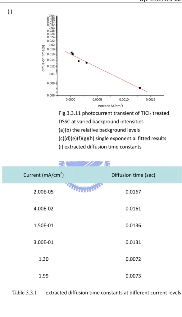
transients were measured under different background illumination intensities. In Fig.3.3.10 (a) and (b), current transient at different photocurrent levels are shown. As the first issue, the perturbation induced increments of current remained the same at low levels since the intensity of the perturbed light was constant and there was a large amount of dye molecules that can provide excited electrons when the background intensity was low and the excited dye molecules were less. On the other hand, when background intensity was raised, the increment of current by the perturbation can no more remain and then visibly decay. In spite of this variation, all the relaxation behaviors of photocurrent can be fitted by a single exponential function well as Fig.3.3.10 (c) – (h). The extracted diffusion time constant is collected in Fig.3.3.10 (i). The increase of diffusion time with the decrease of current level was observed, and the time constant varies from 7ms to 16ms. The reason for longer diffusion time constant values could be related to the increase in depth of effective trapping sites of lower current level.
When the recombination and transport behaviors are understood, it seems the
suggestion of the inhibition effect of TiCl4 treatment on recombination is valid, and it
is necessary to know the origin of the cause. From DOS measurement (Fig.3.3.11), the
Dye Sensitized Solar Cell
38
non-treated. For the porosity of the film is unknown, the intensity was of a relative level, but it was still comparable between the data since the measurement conditions were the same. According to the results, suppression of intensity in deeper levels can be observed, which is thought to be the reason that recombination inhibition is from.
There are two possible speculations of the suppression of surface DOS: first one is that surface state inhibition by Ti bound to surface oxygen site, and thus the second is the effective bonding site increases and bound dye increases. Advanced exploration could be tried to identify these assumptions. Some advanced test methods might be applied to verify the cause of the phenomenon.
Besides, based on available observations, it may be concluded that the transport of excess electrons was mainly inside the nanocrystal since it was slightly affected by the inhibition of density of surface states. Even though the electrical field was limited
by the geometrical boundary conditions, the finitely induced band bending of TiO2 and
coupling between bipyridyl and TiO2 was sufficient to collect excess electrons inside
nanocrystalline bulk, and thus caused higher transport ability than originally expected ones.
Dye Sensitized Solar Cell 39 0 50 0 -1 -2 -3 -4 -5 -6 -7 -8 -9 -10 -11 -12 -13 -14 -15 -16 -17 -18 -19 -20 FTO(2) FTO ITO R e (Z ) (o h m) Re(Z) (ohm) Fig.3.3.1
(a) darkcurrent and (b) photocurrent to voltage
characteristics of DSSC fabricated on different substrates (1) ITO 30 Ω / □ (2) FTO 15 Ω / □ (3) ITO(2) 100 Ω / □
100 150
Re(Z) (ohm)
Fig.3.3.2 EIS of DSSC with different substrate
(1) ITO 30 Ω / □ (2) FTO 15 Ω / □ (3) ITO(2) 100 Ω / □ (a) (b) 0 200 400 600 800 -4000 -3000 -2000 -1000 0 1000 2000 3000 ITO(2) FTO ITO cu rre n t (u A/ cm 2 ) voltage(mV) 0 200 400 600 800 -200 0 200 400 600 800 1000 1200 1400 1600 1800 2000 2200 2400 2600 2800 ITO(2) FTO ITO cu rre n t (u A/ cm 2 ) voltage(mV)
Dye Sensitized Solar Cell 40 30 35 40 45 50 55 0 -2 -4 -6 -8 -10 -12 -14 -16 -18 -20 solvent alpha-terpineol solvent PEG Im(Z ) (o h m) Re(Z) (ohm)
Fig.3.3.3 (a) darkcurrent and (b) photocurrent to voltage
characteristics of DSSC fabricated by different paste solvent (1)alpha-terpineol and (2) poly ethylene glycol
(a)
(b)
Fig.3.3.4
EIS of DSSC by different paste solvent
(1)alpha-terpineol and (2) poly ethylene glycol
0 200 400 600 800 0 500 1000 1500 2000 curr e n t(u A/ cm 2 ) voltage(mV) solvent alpha-terpineol solvent PEG 0 200 400 600 800 -3000 -2000 -1000 0 1000 2000 voltage(mV) cu rre n t(u A/ cm 2 ) solvent alpha-terpineol solvent PEG
Dye Sensitized Solar Cell 41 (c) (b) (a) 0 200 400 600 800 1000 -6000 -4000 -2000 0 2000 4000 6000 8000 10000 cu rre n t ( A/ cm 2 ) voltage (mV) dk PC lt PC dk MPN lt MPN -20 0 20 40 60 80 100 120 140 160 180 200 0 -20 -40 -60 -80 PC MPN Im(Z ) (o h m) Re(Z) (ohm) 10-3 10-2 10-1 100 101 102 103 104 105 106 107 0.0 -0.2 -0.4 -0.6 -0.8 -1.0 MPN PC p h a se (ra d ) frequency (Hz) Fig.3.3.5
(a) dark current and photocurrent to voltage characteristics, (b) EIS, and (c) EIS phase plot of DSSCs using different electrolytic solvent