phys. stat. sol. (a) 204, No. 6, 2077 – 2081 (2007) / DOI 10.1002/pssa.200674766
Paper
GaN alternating current light-emitting device
Hsi-Hsuan Yen*, 1, 2, Wen-Yung Yeh2, and Hao-Chung Kuo1
1 Department of Photonics & Institute of Electro-Optical Engineering, National Chiao Tung University, EE225, 1001, Ta Hsueh Road, Hsinchu, Taiwan 30056, R.O.C.
2 Electronics and Optoelectronics Research Laboratories, Industrial Technology Research Institute, Rm. 206, Bldg. 78, 195, Sec. 4, Chung-Hsing Rd., Chutung, Hsinchu, Taiwan 310, R.O.C.
Received 28 September 2006, revised 30 January 2007, accepted 5 February 2007 Published online 16 May 2007
PACS 78.55.Cr, 78.60.Fi, 85.60.Jb
We report a new design of the light-emitting device which can be operated under alternating current sour-ce directly. The new type alternating current driven light-emitting devisour-ce (AC LED) can increase the radi-tion area in each bias direcradi-tion to improve the device efficiency by the Wheatstone Bridge (WB) circuit design. WB-AC LEDs with different designs were fabricated and the electrical and optical characteristics were measured. It is found that the efficiency of the WB-AC LED is influenced by the varied area ratio of the rectified microchip to the central one because of the different current density and forward bias of each microchip. Additionally, the relationship between the area ratio of microchips and the wall plug efficiency of the WB-AC LED has also been discussed.
© 2007 WILEY-VCH Verlag GmbH & Co. KGaA, Weinheim
1 Introduction
In the recent years, GaN based wide band-gap compound semiconductors have attracted much attention as the commercial productions of light-emitting device (LED). The GaN based LED has been exten-sively used in the variety of applications such as full color display, optical communication, traffic light, and daily lighting [1]. For the case of stationary lighting system, the rectifier is essential to transform the alternating current (AC) applied from the city power company into the direct current (DC) for the LED which can only be operated under DC physically. However, about 30 to 50% input energy will be con-sumed during the AC to DC transformation process because of the poor efficiency. Although there are huge quantity of literatures that concentrated on the increase of the LED’s internal and external quantum efficiency, only few attempts have been made at the research to reduce of energy loss in the AC to DC transformation process of AC into DC, which increases the total wall plug efficiency (WPE) of the whole lighting system.
Numerous microchips integrate into one single LED chip which can be operated under AC source di-rectly has been revealed for several years. The microchips of the current AC LED [2] are grown on sap-phire or other insulated substrates and designed to be connected in parallel and series only. However, only half amount of the microchips in the current AC LED array design radiate every moment, and oth-ers are put out because of under the revoth-ersed bias direction. Furthermore, the flickering frequency of current AC LED design is 50 ~ 60 Hz which is synchronal with the frequency of the input AC source and will make human eyes uncomfortable. The inefficient active layer utility ratio and low flickering fre-quency are both the drawbacks of the current AC LED design.
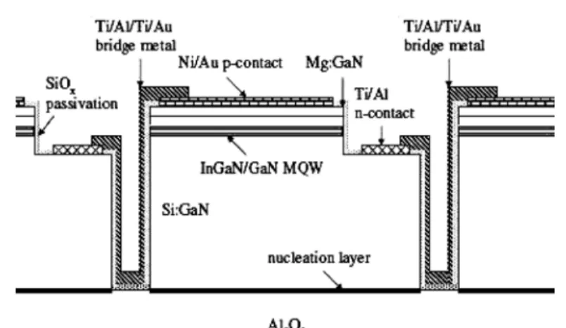
Fig. 1 Schematic of the InGaN–GaN AC LED.
The Wheatstone Bridge (WB) circuit has been applied as the rectifier circuit to transform AC into DC for decades. In this letter, we report the integration of WB circuit concept with the AC LED microchips array design. The electrical and optical properties of the WB-AC LED are also reported.
2 Experiment
The GaN LED samples used were grown on c-face sapphire by the metal-organic chemical vapor deposi-tion (MOCVD). Figure 1 shows the schematic of the InGaN – GaN AC LED structure used in this study. The epitaxial structure consisted of a GaN nucleation layer, a 4 µm thick Si doped n-GaN cladding layer, an InGaN – GaN MQW active layer, an Mg doped p-AlGaN cladding layer, and an Mg doped p-contact layer. The samples were partially etched until the n-type GaN was exposed first, and few meshed areas were etched until the sapphire substrate exposed to achieve the electro-insulation between the microchips. Afterward, the Ni/Au (3 nm/7 nm) contact was evaporated onto the p-type GaN surface served as the transparent p-electrode, and the Ti/Al (50 nm/200 nm) contact was evaporated onto the exposed n-type GaN surface served as the n-electrode, and then the samples were annealed at 550 °C under pure O2 environment in the furnace [3, 4]. Subsequently, a SiO2 (200 nm) layer was deposited onto the samples served as the passivation layer and then was partially etched until the p-contact and n-contact were exposed. The Ti/Al/Ti/Au (100 nm/900 nm/100 nm/200 nm) metal bridge was then evaporated onto the samples to serve as the electrical connection channel between the microchips. One current AC LED and two different WB-AC LED designs (I and II) were fabricated in this study. The dimensions of these LEDs were all 750 µm × 750 µm. Figure 2(a) shows the current AC LED array circuit diagram. Every two microchips connect in parallel of opposite directions and each pair of the microchips connects with others in series. While the AC source alternates the direction of voltage bias
Fig. 2 Circuit diagrams of the (a) current and (b) WB-AC LED.
phys. stat. sol. (a) 204, No. 6 (2007) 2079
Paper
(a) (b) (c)
Fig. 3 (online colour at: www.pss-a.com) Photographs of the (a) current AC LED, (b) WB-AC LED I, and (c) WB-AC LED II.
every moment, only half amount of the microchips radiate in the state of forward bias and others are switched off simultaneously. Figure 2(b) shows the circuit diagram of the WB-AC LED that integrates the Wheatstone bridge circuit into the microchips arrangement. There are 55 microchips in the WB-AC LED array disposed as the Wheatstone bridge circuit. Four groups of the microchips, which contain 10 microchips in each of them, are around the WB-AC LED and taken as the rectifiers to transform the AC into DC. These four groups of the microchips make the other 15 microchips in the center of the WB-AC LED always under the forward bias whether the alternating bias direction is. There are 20 rectified and 15 central microchips, which are more than the half amount of 55 microchips in the WB-AC LED array, radiated light in each bias direction.
3 Results and discussion
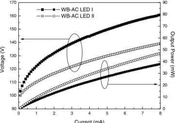
Figure 3(a), (b), and (c) show the photographs of the current AC LED and two WB-AC LEDs operated under 1 mA DC input. The radiated area ratio of the rectified microchip to central one was 1 : 24 of WB-AC LED I and 1 : 2 of WB-WB-AC LED II, respectively. The radiation area increases 136.4% of WB-WB-AC LED I and 84.4% of WB-AC LED II than the current AC LED design, respectively. The AC LED array, which integrates the concept of WB circuit, achieves the higher active layer utility ratio than the current AC LED design, and the radiation area of the WB-AC LED I is 28.3% larger than WB-AC LED II under DC operated. 0 1 2 3 4 5 6 7 8 90 100 110 120 130 140 150 160 170 WB-AC LED I WB-AC LED II 0 10 20 30 40 50 60 70 80 90 O u tput P o w e r (mW ) Current (mA) V o lt age (V )
Fig. 4 Current–voltage (I–V) and the output power characteristics of the WB-AC LED I and II meas-ured under DC source.
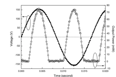
0.000 0.005 0.010 0.015 0.020 -150 -100 -50 0 Time (second) V o lt age -10 0 10 20 30 o w e r (mW )
Fig. 5 Time-variant input voltage and output power characteristics of WB-AC LED II.
Figure 4 shows the forward I–V and the output power characteristics of the WB-AC LED I and II under DC source. It can be seen that the forward voltage at 2 mA is 131.9 V of WB-AC LED I and 116.7 V of WB-AC LED II, and the output power is 33 mW of WB-AC LED I and 44 mW of WB-AC LED II under the identical input power 1 W, respectively. It is found that the WPE of WB-AC LED I is lower than WB-AC LED II, even the radiation area of WB-AC LED I is larger than WB-AC LED II, which can be attributed to the current density of the rectified microchip is 896 A/cm2 in WB-LED I and 162 A/cm2 in WB-AC LED II under the identical input power 1 W, respectively. The higher current density of the rectified microchip in WB-AC LED I than WB-AC LED II causes the lower internal quan-tum efficiency and higher forward voltage that reduce the WPE of WB-AC LED I simultaneously. Figure 5 shows the time-variant input voltage and the output power characteristics of the WB-AC LED II driven by the AC 110 V source. The variance of the input AC source voltage is from 155 to – 155 V and the frequency is 60 Hz.
The WB-AC LED II radiates only after the input voltage higher than the sum of microchips’ threshold voltage, which is about 100 V, and the lighting duty cycle of the WB-AC LED II is 60%. From Fig. 6, it is found that the WPE of the WB-AC LED II is 4.3% and the averaged input power is 0.64 W under AC 110 V operated, but the WPE of the WB-AC LED II with the identical input power under DC operated is 5.3%. It is speculated that the fluctuant output power caused by the AC source will decrease the effi-ciency of WB-AC LED.
0.000 0.005 0.010 0.015 0.020 0.0 0.2 0.4 0.6 0.8 1.0 1.2 1.4 1.6 1.8 2.0 2.2 2.4 Po w e r (W) Time (second) Input power
WB-AC LED II output power
Fig. 6 (online colour at: www.pss-a.com) Rela-tionship between the input power and output power of WB-AC LED II.
phys. stat. sol. (a) 204, No. 6 (2007) 2081
Paper
4 Summary
We fabricated the WB-AC LED integrated the concept of Wheatstone bridge circuit into AC LED array design. It was found that the active layer utility ratio increased 136.4% of WB-AC LED I and 84.4% of AC LED II than the current AC LED design, respectively. The output power was 33 mW of WB-AC LED I and 44 mW of WB-WB-AC LED II under the DC input power 1 W, respectively, and the WPE of the WB-AC LED II was 4.3% under AC 110 V operated directly. These results suggest that one can unify the microchips’ area to minimize the current density of the microchips and improve the efficiency of WB-AC LED.
References
[1] S. Nakamura and G. Fasol, The Blue Laser Diodes: GaN Based Light Emitters and Lasers (Springer-Verlag, Berlin, 1997).
[2] Jin-Ping Ao, H. Sato, T. Mizobuchi, K. Marioka, S. Kawano, Y. Muramoto, Young-Bae Lee, D. Sato, Y. Ohno, and S. Sakai, phys. stat. sol. (a) 194(2), 376 – 379 (2002).
[3] S. Murai, H. Masuda, Y. Koide, and M. Murakami, Appl. Phys. Lett. 80(16), 2934 (2002).
[4] Jin-Kuo Ho, Chamg-Shyang Jong, Chien C. Chiu, Chao-Nien Huang, Chin-Yuen Chen, and Kwang-Kuo Shih, Appl. Phys. Lett. 74(9), 1275 (1999).