Indium Aggregated Quantum Dot Structures in InGaN Compounds
C. C. Yang, Shih-Wei Feng, Yung-Chen Cheng, Yi-Yin Chung, En-Chiang Lin,Hsiang-Chen Wang, Tsung-Yi Tang, Chih-Chung Deng, and Si-Jiung Lin Graduate Institute of Electro-Optical Engineering, Department of Electrical Engineering and
Graduate Institute of Electronics Engineering, National Taiwan University. I , Roosevelt Road, Sec. 4, Taipei
(phone) 886-2-23657624
flm)
886-2-23652637 (E-maiS) [email protected] Kung-Jen MaDepartment of Mechanical Engineering, Chung Hua UniversiQ, Hsinchu Yen-Sheng Lin
Department of Mechanical Engineering, Chung Cheng Institute of Technology, Tahsi, Taoyuan
Abstract -- We will summarize the optical characteristics and microsmctures of the indium-aggregated quantum dots in InGaN compounds, including intended InGaN/GaN quantum well structures and InGaN epi-layers. In quantum well structures, the dependencies of optical properties and material structures on well width and nominal indium content are to be discussed. Also, the effects of silicon doping will be reported. Furthermore, the effects ofpost-growth thermal annealing on the formation of quantum dot-like structures and their variations of optical properties will be presented In InGaN epi-layers. we have studied the optical and
material properties of such films with high indium contents. From the images of cathodo-luminescence and high-resolution hansmission electron microscopy, quantum dot structures could be observed. Afer thermal annealing, the original yellow emission became blue in color in one of the samples. In the other sample, the original red emission became the combination of red, yellow and blue photons, leading to white in color.
1. Introduction
Indium-rich cluster formation in InGaN/GaN quantum well (QW) structures results in potential fluctuations and hence the effect of canier localization [1],[2]. On the other hand, the large lattice mismatch between
InGaN
wells and GaN barriers leads to significant strains in the well layers. The strain-induced piezoelectric field, which generates the quantum confined Stark effect (QCSE), has also been used for explaining measured optical phenomena, such as the excitation power dependence of PL spectral peak [3],[4].In
this effect, electrons and holes are spatially separated. Hence, radiative transition rate is reduced and PL decay time is elongated. In this paper, we report the different thermal annealing results in InGaN/GaN QW structures of different nominal indium contents and different QW widths. Various optical characterization and material analyses were conducted to reveal the photon emission behaviors under different conditions. The two sets of samples were grown on c-plane sapphire with MOCVD. Following the deposition of 30 nm GaN27 0-7803-7887-3/03/$17.00 02003 IEEE
buffer layer and a 2.3 pm GaN layer, QW structures consisting of five pairs of InGaN well and 10 nm-thick GaN bamer were grown. In the first set of sample, three samples of the same QW geometry of 2.5 nm in well width but different nominal indium contents (with lower to higher indium contents designated as samples A, B, and C) were prepared. In the second set of sample, three samples of the same nominal indium content hut different well widths at 2,3, and 4 nm were prepared and referred to as samples w20, w30 and w40, respectively. The growth temperatures were 1010 and 720 'C for GaN and InGaN, respectively.
As-grown samples were thermally annealed
in a quartz tube fumace at different temperatures ranging from 800 to 900 "C in nitrogen ambient for 30 min.
2. Indium Content Dependence
Fig. 1 shows the dependencies of photoluminescence (PL) spectral peak position on sample temperature for various samples and under various thermal annealing conditions. One can see that generally PL spectral peak blue shifts upon
thermal annealing in each sample. Such a blue shift is particularly significant in sample A, which has the lowest indium content. In this figure, the data points in a few cases are incomplete because of the difficulty in determining the spectral peak position at high sample temperatures. Careful examination reveals that all the curves in Fig. 1 of complete data points show S-shape variations, which were believed to be the features of carrier localization and QCSE. For the samples of lower indium contents (Samples A and B), higher thermal annealing temperatures lead to larger blue shift. However, for sample C of higher indium content, 800 "C results in the largest blue shift. Fig. 2 shows the variations of normalized integrated PL intensity with temperature of various conditions. Such a variation is usually used for representing the radiative efficiency of a sample. One can see that generally thermal
annealing results in high radiative efficiency except the case of 850 OC annealing of sample C.
Fig. 3 shows the variations of activation energy upon thermal annealing. First, we observe that the activation energy is larger for a sample of lower indium content. Meanwhile, generally thermal annealing results in the reduction of activation energy. The variation trend of activation energy in Fig. 3 is generally consistent with the radiative efficiency behaviors in Fig. 2. Fig. 4 shows the Stokes shift variations with temperature of various conditions. All the
three samples demonstrate the same trend. Upon thermal annealing at 800 'C, the Stokes shift is reduced. However, increasing thermal annealing temperature results in increasing
Stokes
shift. The valueof
a Stokes shift is usually used to represent the extent of indium aggregation or the strengthof piezoelectric field (OCSE).
3. Quantum Well Width Dependence
PL spectral peak variations with temperature of the three samples of different QW widths under various thermal annealing conditions are shown in Fig. 5 . After
thermal annealing, the S-shape variation of PL peak is maintained in each case. Thermal annealing results in blue shifts of PL peak in w20 and red shifts in w30 and w40. Also, in all samples thermal annealing at 800 'C leads to the largest spectral shifts. As thermal annealing temperature increases, the blue shift or red shift is reduced. Fig. 6 shows the temperature-dependent variations of integrated PL intensity of the as-grown and annealed samples. The integrated PL intensities were enhanced upon thermal annealing in w20 and w30, particularly significant in w20. However, that of w40 was reduced. From Figs. 5 and 6 , it is interesting to note that the trends of PL peak shifts (blue or red) and integrated PL intensity variations (increase or decrease) with annealing temperature are the same in each of the three samples. Thermal annealing at 800 "C always leads to the largest changes. As annealing temperature increases, optical properties generally tend to return to the as-grown condition. However, it is noted that in w20 and w40, the curves of PL peak and integrated PL intensity of 900 'C annealing lie between those of 800 and 850 "C annealing. Nevertheless, in w30 the curves of 850 O C
annealing lie between those of 800 and 900 OC annealing. This difference indicates different dependencies on annealing temperature of various samples.
4. High Indium Content Samples
We report the thermal annealing effects on the optical and material characteristics of a high-indium InGaN film with luminescence in the yellow range. It was observed that after thermal annealing, the PL peak shifted
from the
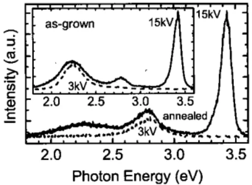
yellow band into the blue range. The spectral change was attributed to the reduction of cluster size upon thermal annealing. The sample used in this study was grown in a low-pressure MOCVD. A -1.2 pm GaN layer was deposited on a sapphire substrate with a 25 nm GaN buffer layer. The GaN layer growth was followed by the deposition of an InGaN film with a thickness of -0.2 pm. Thenominal indium content was estimated to be higher than 30 %. Thermal annealing was conducted with 800 'C for 30 min in ambient nitrogen. Fig. 7 shows the PL and PLE spectra at 10K of the as-grown and annealed samples. The PL spectral peak has shifted from the yellow band (around 2.2eV) to the blue band (around 2.75eV) after thermal annealing. The blue emission contribution as a small side-lobe can also be observed in the PL spectrum of the as-grown sample. Fig. 8 shows the cathodo-luminescence spectra of the as-grown and annealed samples. In each sample, the 15kV and 3kV curves represent the results of using different electron acceleration voltages for deeper and shallower luminescence generations. In the as-grown sample, only the luminescence in the yellow band is observed in a shallow layer. However, with 15 kV electrons, not only the strong luminescence of the GaN layer (around 2.4eV) can be seen, but also a small peak of blue luminescence can be observed. Hence, it is expected that a certain microstructure existing deep in the InGaN film can emit photons in the blue range. After thermal annealing, in the shallow layer of InGaN (3kV probe), only the blue luminescence exists that is consistent with the PL measurement. With higher energy electron excitation, the blue luminescence is enhanced and the GaN emission peak appears. HRTEM images showed that the
domain size in the annealed sample is smaller. Also, the domain density becomes higher after thermal annealing. Hence, we can assume that during thermal annealing, spinodal decomposition tends to break large clusters into smaller ones. In this process, the indium content in an InGaN cluster can be enhanced, leading to a smaller material band gap. However, the shrinkage of cluster size results in stronger quantum confinement and increases the effective band gap of the quantum dot. The quantum confinement effect may overcome the contradictory trend of indium content increase and result in a significant blue shift in PL spectrum.
References
[l] Y. Narukawa, Y. Kawakami, M. funato,
S. Fujita, S . Fujita and S. Nakamura, Appl. Phys. Lett. 70, 981-983 (1997).
[2] M. D. McCluskey, L. T. Romano, B. S . Krusor, D. P. Bour, N. M. Johnson and S. Brennan, Appl. Phys. Lett. 72, 1730-1732 (1998).
[3] P. Riblet, H. Hirayama, A. Kinoshita, A. Hirata, T. Sugano, and Y. Aoyagi, Appl. Phys. Lett. 15,2241-2243 (1999).
[4] S . F. Chichibu, A. C. Abare, M. S .
Minsky, S. Keller, S. B. Fleischer, J. E. Bowers, E. Hu, U. K. Mishra, L. A. Coldren, and S. P. DenBaars, T. Sota, Appl. Phys. Lett. 73,2006-2008 (1998) 2'3
1
A'
850°C8oO'c
1
.
900°C 4. . .
0 50 1w 150 200 250 303 2 . 2 . ,.
, . , . ,.
, . I . , , 0 50 100 150 200 250 300 Temperature (K) Temperature (K)Fig. 1 PL spectral peak positions versus temperature. Fig. 2 Integrated PL intensities versus temperahue.
A
*.
I ; f B 1**
*
,
*.
t,
C:
I a s g m 800'C A 850'C v SWQCB 444
-.
2.90 - 2 8 5 - % .-
6 2.80 .- +..g
2.70 2.65 2.60 2.55 a A L--.
* - _ ... ... c .....
..
-
-m-aa-gmwn d 8 5 O e J -8OO(J -9OOeJ .-.-.
--n-.-.-.-.
-.-.--.-.-.-._.
2 . 7 5 : z:
1
1
:
:
iYw3'
-
: ~ * z - ' - ' - ' L o-
--.
-
"-
w40 0 ' ' ' ' ' ' ' I ' I " 1 12 I I I 1 as-gwn 800'C 850'C 900'C . . . - 7 ,._...A..
. .__..' ... c..,
E U) U) Y 0 B . ..._... - - - * - m 300 t I t I 6 0 0 4 - 7 ,._...A..
'. ... .__..' U) U) B . ..._... - - - * - m i400u
300Fig. 3 Activation energies under different conditions. Fig. 4 Stokes shifts under different conditions.
Photon Energy (eV)
Fig. 7 PL and PLE spectra of the as-grown and annealed sample Y .
. . . 0 50 loo 150 MO 250 3w
Tempemure (K)
Fig. 6 Integrated PL intensities versus temperature.
2.0
2.5
3.0
3.5
Photon Energy (eV)
Fig. 8 Cathodo-luminescence spectra o f the as-grown and annealed sample Y .