Mechanical strain effect of n-channel polycrystalline silicon
thin-film transistors
C.-F. Huang, Y.-J. Yang, C.-Y. Peng, F. Yuan, and C. W. Liua兲
Department of Electrical Engineering, National Taiwan University, Taipei, Taiwan 106,
Republic of China and Graduate Institute of Electronics Engineering, National Taiwan University, Taipei, Taiwan 106, Republic of China
共Received 13 February 2006; accepted 10 July 2006; published online 5 September 2006兲 The current change of n-channel polycrystalline silicon thin-film transistors is analyzed experimentally and theoretically under different strain conditions. Under the uniaxial strain parallel to the channel, the +6.7% and +5.3% drain current enhancements are achieved in linear and saturation regions, respectively. There are −4.4% 共linear兲 and −4.6% 共saturation兲 drain current degradations when the uniaxial strain is applied perpendicular to the channel. The polycrystalline silicon is mainly composed of 共111兲-oriented grains, measured by electron diffraction pattern. Phonon-limited mobility is theoretically calculated. There is a qualitative agreement between experiments and theoretical analysis. © 2006 American Institute of Physics.
关DOI:10.1063/1.2344855兴
Most display technology is based on amorphous Si thin-film transistors共TFTs兲, but polycrystalline silicon 共poly-Si兲 TFTs have attracted a great attention in recent years due to much higher carrier mobility. The low temperature polycrys-talline silicon共LTPS兲 TFTs have much higher electron mo-bility共= 100– 300 cm2/ V s兲 and better reliability as com-pared to conventional amorphous Si TFTs 共= 1 cm2/ V s兲. Strained-Si technology has been used extensively in the Si industry for 90 nm and beyond. The mechanical strain ef-fects on complementary metal-oxide semiconductor and op-tical devices have been reported.1–7However, no strain effect on poly-Si TFTs was reported in the past. The electrical per-formance of poly-Si TFTs is investigated under different strain conditions.
The LTPS poly-Si TFTs are fabricated with top-gated structure.8The amorphous Si layer is deposited using radio frequency plasma-enhanced chemical vapor deposition sys-tem, and excimer laser crystallization technique is used to form poly-Si film with a grain size of ⬃0.3m. The tran-sistor is fabricated after gate patterning and source/drain for-mation. The effective oxide thickness is 100 nm. The effec-tive electron mobility of poly-Si TFTs is⬃125 cm2/ V s. The mobility is extracted by using the conventional square law current model from the IDS-VDScurve. The extracted mobil-ity is comparable to the value in the literatures.9,10The esti-mated gate-channel capacitance Cgc 共⬃0.07 pF兲 is beyond the measurement limit of our meter due to the small area. Therefore, the split capacitance-voltage technique used in the strained-Si field effect transistors cannot be conducted in this case.
The mechanical setup to apply external strain was re-ported previously.11,12For single crystalline Si, the level of external strain was measured by Raman spectroscopy and was consistent with finite element simulation by ANSYS.13 The poly-Si has a built-in tensile stress of ⬃1 GPa 共⬃0.44%兲,14 measured by the Raman shift of 6.5 cm−1 as compared to bulk Si. The apparent strains are calculated to
be ⬃0.15% and ⬃0.17% for uniaxial and biaxial strains, respectively, by the finite element method. However, the poly-Si film is in elastic strain as grown, and the wafer pos-sesses curvature even before bending. Therefore, it may be difficult to quantify the strain level using Raman.
Figure 1 shows the drain current共IDS兲 versus drain volt-age共VDS兲 of n-channel TFTs. The gate width and length are 20 and 10m, respectively. The drain currents under uniaxial tensile strain have +6.7% and +5.3% enhancements in the linear region and saturation region, respectively, for the strain parallel to the channel共longitudinal strain兲. How-ever, the drain currents are degraded −4.4% and −4.6% for linear region and saturation region, respectively, for the uniaxial tensile strain perpendicular to the channel 共trans-verse strain兲. For the linear region, the drain current change is measured at VGS-VTH= 10 V and VDS= 5 V, and for the saturation region, current change is measured at VDS= 10 V. The drain current change under various strain conditions is shown in Fig. 2. As longitudinal strain is applied, the drain current increases with increasing strain, whereas the drain current degraded gradually with increasing transverse strain. However, the current change is within 1% for the external biaxial strain. The sensitivity of drain current to strain共兲 is defined as S共IDS兲=⌬IDS/IDS. The S共IDS兲=35 and −31 for longitudinal strain and transverse strain, respectively. The S 共IDS兲 is much higher than previously reported values of amorphous TFTs.15
a兲Author to whom correspondence should be addressed; electronic mail:
[email protected] FIG. 1. Output characteristics of poly-Si TFTs under uniaxial tensile strain. APPLIED PHYSICS LETTERS 89, 103502共2006兲
0003-6951/2006/89共10兲/103502/3/$23.00 89, 103502-1 © 2006 American Institute of Physics Downloaded 13 Feb 2009 to 140.112.113.225. Redistribution subject to AIP license or copyright; see http://apl.aip.org/apl/copyright.jsp
The electron diffraction pattern of transmission electron microscopy共TEM兲 is used to investigate the crystal orienta-tion of the poly-Si film on glass. The plane view TEM image is shown in Fig. 3. From the electron diffraction pattern of poly-Si grain共the inset of Fig. 3兲, the poly-Si film is mainly composed of 共111兲-oriented grains,16 which is consistent with the powder x-ray diffraction共not shown兲.
The phonon-limited electron mobility in the single crys-talline Si under biaxial/uniaxial strain on 共001兲, 共110兲, and 共111兲 grains is theoretically calculated.17,18
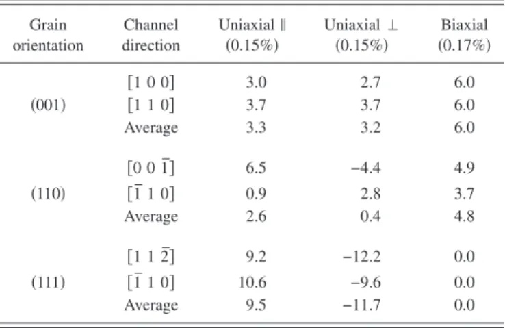
The accuracy of our theoretical calculation is calibrated with the previous work of the strained-Si field effect transistors,6,19 and gives the reasonable estimation of mobility data.7,11,12 The calcu-lated mobility changes due to external biaxial/uniaxial strain on various grain orientations are shown in Table I. The built-in biaxial strain in the poly-Si film is considered in the calculation, and the mobility change in the table is solely due to the external mechanical strain. For the channel length of 10m with the grain size of⬃0.3m, the electron travels many 共111兲 grains with different in-plane direction. There-fore, the average mobility over all possible grain directions has to be considered. For共111兲 grain orientation, the average mobility has 9.5% enhancement for longitudinal strain, but has −11.7% degradation for transverse strain. The trend is consistent with experimental data 共5.3% for longitudinal strain and −4.6% for transverse strain兲, but the absolute
mag-nitude is lower. The reason for the deviation from the model is unclear. The discrepancy between the data and the calcu-lation might be attributed to the existence of a small fraction of other grains besides共111兲. The theoretical average mobil-ity of共001兲 and 共110兲 grain orientations shows a completely different trend with our data, indicating that the grain orien-tation in the poly-Si film is mainly 共111兲 oriented and is consistent with the electron diffraction pattern and x-ray dif-fraction.
The channel direction is along 具112¯典 as an example to explain the mechanism of mobility change due to strain关Fig. 4共a兲兴. For the longitudinal strain 关Fig. 4共b兲兴, valleys 1 and 2 shift to higher energy level than other valleys. Most electrons are populated in the lower energy valleys 共shaded area兲. Therefore, the lighter effective mass of the lower energy val-leys is responsible for the mobility enhancement. However, for the transverse strain关Fig. 4共c兲兴, most electrons locate in valleys 1 and 2 due to their lower energy levels, and the heavier effective mass along 具112¯典 leads to mobility degradation.3,18The average mobility over all possible direc-tions should be calculated due to the different grains along the channel.
The strain effect of n-channel poly-Si TFTs is investi-gated. The electrical performance can be further enhanced with external mechanical strain. The low cost and reasonable performance enhancement by the external mechanical bend-ing is beneficial for the future flat panel display technology. The National Taiwan University group is supported by the National Science Council of Taiwan under Contract No. FIG. 2. Drain current change vs various apparent strains. The apparent
strain is the strain calculated by finite element method.
FIG. 3. Plane view TEM image of poly-Si film. The electron diffraction pattern shows that the film is mainly composed of共111兲-oriented grains.
TABLE I. Mobility change共%兲 of single crystalline Si under tensile stress. The built-in stress of⬃1 GPa in poly-Si film is considered in the calcula-tion, and the mobility change is due to the external mechanical strain. The average mobility is the mean value for all possible channel directions.
Grain orientation Channel direction Uniaxial储 共0.15%兲 Uniaxial⬜ 共0.15%兲 Biaxial 共0.17%兲 关1 0 0兴 3.0 2.7 6.0 共001兲 关1 1 0兴 3.7 3.7 6.0 Average 3.3 3.2 6.0 关0 0 1¯兴 6.5 −4.4 4.9 共110兲 关1¯ 1 0兴 0.9 2.8 3.7 Average 2.6 0.4 4.8 关1 1 2¯兴 9.2 −12.2 0.0 共111兲 关1¯ 1 0兴 10.6 −9.6 0.0 Average 9.5 −11.7 0.0
FIG. 4. 共a兲 Two specific channel directions of 共111兲-oriented Si. The pro-jection of constant-energy contour of共111兲 Si conduction band under 共b兲 longitudinal strain and共c兲 transverse strain. Most electrons locate in the lower energy valley under uniaxial strain共shaded area兲.
103502-2 Huang et al. Appl. Phys. Lett. 89, 103502共2006兲
NSC 94-2215-E-002-040. The authors would like to thank S. T. Chang 共National Chung Hsing University, Taiwan, R.O.C.兲 for the helpful discussion. The fabrication of chip by Toppoly Optoelectronics Corp., Taiwan, is highly appreciated.
1S. E. Thompson, G. Sun, K. Wu, J. Lim, and T. Nishida, Tech. Dig. - Int.
Electron Devices Meet. 2004, 221.
2S. Maikap, C.-Y. Yu, S.-R. Jan, M. H. Lee, and C. W. Liu, IEEE Electron
Device Lett. 25, 40共2004兲.
3C. W. Liu, S. Maikap, and C.-Y. Yu, IEEE Circuits Devices Mag. 21, 21
共2005兲.
4F. Yuan, S.-R. Jan, S. Maikap, Y.-H. Liu, C.-S. Liang, and C. W. Liu, IEEE
Electron Device Lett. 25, 483共2004兲.
5F. Yuan, C.-F. Huang, M.-H. Yu, and C. W. Liu, IEEE Trans. Electron
Devices 53, 724共2006兲.
6H. Irie, K. Kita, K. Kyuno, and A. Toriumi, Tech. Dig. - Int. Electron
Devices Meet. 2004, 225.
7S. Maikap, M. H. Liao, F. Yuan, M. H. Lee, C.-F. Huang, S. T. Chang, and
C. W. Liu, Tech. Dig. - Int. Electron Devices Meet. 2004, 233.
8K. Tanaka, H. Arai, and S. Kohda, IEEE Electron Device Lett. 9, 23
共1988兲.
9K. C. Moon, J.-H. Lee, and M.-K. Han, IEEE Trans. Electron Devices 52,
512共2005兲.
10S.-M. Han, M.-C. Lee, M.-Y. Shin, J.-H. Park, and M.-K. Han, Proc. IEEE
93, 1297共2005兲.
11M. H. Liao, M. J. Chen, T. C. Chen, P. L. Wang, and C. W. Liu, Appl.
Phys. Lett. 86, 223502共2005兲.
12M. H. Liao, S. T. Chang, M. H. Lee, S. Maikap, and C. W. Liu, J. Appl.
Phys. 98, 066104共2005兲.
13M. H. Liao, C.-Y. Yu, C.-F. Huang, C.-H. Lin, C.-J. Lee, M.-H. Yu, S. T.
Chang, C.-Y. Liang, C.-Y. Lee, T.-H. Guo, C.-C. Chang, and C. W. Liu, Tech. Dig. - Int. Electron Devices Meet. 2005, 1023.
14P. Lengsfeld, N. H. Nickel, Ch. Genzel, and W. Fuhs, J. Appl. Phys. 91,
9128共2002兲.
15P. Servati and A. Nathan, Proc. IEEE 93, 1257共2005兲.
16S. Christiansen, P. Lengsfeld, J. Krinke, M. Nerding, N. H. Nickel, and H.
P. Strunk, J. Appl. Phys. 89, 5348共2001兲.
17S. Takagi, Judy L. Hoyt, Jeffrey J. Welser, and James F. Gibbons, J. Appl.
Phys. 80, 1567共1996兲.
18I.-J. Yang, C.-Y. Peng, S. T. Chang, and C. W. Liu, International
Semicon-ductor Device Research Symposium, 2005 p. 187.
19K. Uchida, T. Krishnamohan, K. C. Saraswat, and Y. Nishi, Tech. Dig.
-Int. Electron Devices Meet. 2005, 135.
103502-3 Huang et al. Appl. Phys. Lett. 89, 103502共2006兲