國
立
交
通
大
學
電控工程研究所
碩
士
論
文
模組化非線性運算放大器增益所產生之
諧波失真與模組設計最佳化運用在積分
三角類比數位轉換器
Modeling Harmonic Distortions Caused by Nonlinear Op-Amp
DC-Gain and Model-based Design Optimization for Sigma-Delta
Modulators
研 究 生:謝智隆
指導教授:陳福川 教授
模組化非線性運算放大器增益所產生之諧波失真與
模組最佳化在離散時間積分三角類比數位轉換器
Modeling Harmonic Distortions Caused by Nonlinear Op-Amp
DC-Gain and Model-based Design Optimization for Sigma-Delta
Modulators
研 究 生:謝智隆 Student:Chih-Lung Hsieh
指導教授:陳福川 Advisor:Fu-Chuang Chen
國 立 交 通 大 學
電 控 工 程 研 究 所
碩 士 論 文
A ThesisSubmitted to Department of Electrical and Control Engineering College of Electrical Engineering and Computer Science
National Chiao Tung University in partial Fulfillment of the Requirements
for the Degree of Master
in
Electrical and Control Engineering
September2009
Hsinchu, Taiwan, Republic of China
模組化非線性運算放大器增益所產生之諧波失真與
模組最佳化在離散時間積分三角類比數位轉換器
研究生:謝智隆 指導教授:陳福川 教授 國立交通大學 電控工程研究所摘要
傳統的積分三角類比數位轉換器電路規格設計是一個相當耗時的工作,且需要不斷 的嘗試各種電路規格,以達到所需要的解析度。本篇論文分析了各種不同架構的積分 三角類比數位轉換器之主要雜訊來源與非線性特性所造成的失真問題。藉由分析推導 出的失真功率模型、雜訊功率模型及絕對功率消耗模型,並以訊號對雜訊和失真比 (SNDR)來當作我們的設計規格,以做最佳化的設計。此最佳化設計意指在特定系統規 格下(如頻寬、訊號對雜訊和失真比),找到一組最佳化的設計參數,使得類比數位轉 換器的功率消耗最小以及訊號對雜訊和失真比最大,並節省龐大制定電路規格的時間 成本。最後我們將針對已發表的設計結果來做驗證的工作。雖然現今已存在相當多行 為模擬工具以自動化制定電路規格,但較之下,本論文所提出的最佳化方法將快上許 多。Modeling Harmonic Distortions Caused by
Nonlinear Op-Amp DC-Gain and Model-based
Design Optimization for Sigma-Delta Modulators
Student:Chih-Lung Hsieh Advisor:Dr. Fu-Chuang Chen
Institute of Electrical and Control Engineering Nation Chiao Tung University
ABSTRACT
The conventional sigma-delta ADC design approach is a time consuming process and needs much trials and errors. This paper analyze the mainly noise sources and nonlinear distortions. Utilizing the noise power models, nonlinear distortion power models and accurate power consumption models derived in this paper, and the assigned signal to noise and distortion ratio (SNDR) to be the design goal, we can forward to do design optimization under the specific specifications. Design optimization means that under the specific specifications (signal bandwidth, SNDR), we find a set of optimal design parameters such that the power consumption of ADCs is minimum and SNDR is maximum, and reduce the huge time-cost to set up the circuit specifications. Finally, design optimization is tested against a published design result. Although design automation issues have been partially addressed by recent behavior- simulation–based methods, yet such methods can be slower than our analytical approach far.
誌謝 Acknowledgment
我要將此論文獻給 我親愛的母親-江麗金 女士 最疼我的父親-謝朝榮 先生 若沒有他們,我不可能有機會完成此篇論文,並且從交通大學碩士班畢業。此外, 必須感謝指導教授陳福川博士兩年來嚴格的督促與指導,讓我學會做研究的方法與心 態。另外,也要感謝口試委員林清安教授、洪浩喬教授與陳科宏教授對本篇論文所給 予的建議與指導。 還要感謝實驗室文佑學長在我一年級時幫我打好深厚的研究基礎。感謝實驗室同 瑞祺、武璋和學弟子恩、嘉昌陪我度過最後的學生生涯,並在研究上給予我很多幫助。 感謝學弟們,謝謝你們在這兩年間帶給我的鼓勵和歡樂,我以後會很懷念晚上打棒球 的日子。最後要謝謝這兩年在新竹唸書期間所有幫助過我的人,雖然無法一一列舉, 但在這邊向大家致上最大的謝意。Contents
中文摘要 ... I English Abstract ... II Acknowledgment... III Contents ...IV Lists of Tables ...VII Lists of Figures ...IX List of Symbols ...XIII
Chapter1 Introduction ...1
1.1 Current Status and Background ... 1
1.2 Motivation and Aims ... 1
1.3 Organization ... 3
Chapter2 Fundamental Theorems of Sigma-Delta Modulators ... 5
2.1 Nyquist Sampling Theorm ... 5
2.2 Quantization Noise and Peak SNR ... 7
2.3 Techniques of Sigma-Delta Modulator ... 9
2.3.1 Oversampling Technique ... 9
2.3.2 Noise shaping ... 11
Chapter3 Architectures of Sigma-Delta Modulator ... 13
3.1 First-Order Sigma-Delta Modulator ... 14
3.2 Single-Loop Second-Order Sigma-Delta Modulator ... 16
3.3 Single-Loop High Order Sigma-Delta Modulator ...17
3.4 InterpolativeSigma-Delta Modulator ... 18
3.5 MASH Architecture ... 19
3.7 Multi-bit Sigma-Delta Modulator use DEM Technique ... 22
3.7.1 Randomization Technique ... 23
3.7.2 Data Weighted Averaging (DWA) ……... 23
3.8 Decimator ... 25
3.9 Performance Metrics for a ΣΔ Modulator ... 26
Chapter4 Discuss About Different Architecture of Non-idealities Noise and Distortion Models……….…...28
Chapter5 Op-amp Non-Linear Gain Curve...………29
5.1 DC-gain Distortion Can Be Severe …... 29
5.2 Modeling Nonlinear DC-gain Curves ………... 29
5.3 Verifying Nonlinear DC-Gain Curve Model………..31
Chapter6 SDM DISTORTION DUE TO THE NONLINEAR DC-GAIN OF THE OPERATIONAL AMPLIFIER………...34
6.1 Properties of VS ...34
6.2 Transfer Characteristics of the First Integrator...35
6.3 Nonlinear DC-gain Distortions at SDM Output ...37
6.4 Behaving Model Simulation Results …………...39
6.5 Transistor Level Simulation Results………...41
Chapter7 THE DESIGN OPTIMIZATION BETWEEN MODEL-BASED AND SIMULATION-BASED………...43
7.1 How to Generate SNDR of Simulation-based SDM Approach and Run OPTIMIZATION ...44
7.2 How to Generate SNDR of Model-based SDM Approach and Run OPTIMIZATION...45
7.3 Comparisons With These Two Optimization Schemes ...45
7.3.1 Model-based V.S. Simulation-based………...45
7.3.2 Speed………...46
Chapter8 Design Optimization of Sigma-Delta ADCs Design ...47
8.2 Design Parameters Discussions ...49
Chapter9 Optimization Simulation Results ...51
9.1 ΣΔ ADC for ADSL-CO Applications ………51
9.2 ΣΔ ADC for 14-bit 2.2-MS/s………..54
Chapter10 Conclusions and Future Works ...56
Lists of Tables
TABLE 6.1 The relationship between the each parameter and the harmonic distortion
... 38
TABLE 6.2 Minimum requiredAO and OSR ... 39
TABLE 6.3 Comparison of theoretic result and behavior simulation of Case A……...…...40
TABLE 6.4 Comparison of theoretic result and behavior simulation of Case B... 41
TABLE 6.5 Comparison of theoretic result and behavior simulation of Case C... 41
TABLE 6.6 Comparison of theoretic result and Spice simulation………....42
TABLE 7.1 SIMULATION TIMES FOR THE PROPOSED MODELS……… 46
TABLE 8.1 The representation of each noise in our models……….48
TABLE 8.2 The representation of each parameter in our models………... 49
TABLE 8.3 Summary of noise and distortion-power and power-rating when design parameters increase………50
TABLE 9.1 Comparisons of our design results with those in [3]………..52
TABLE 9.2 The corresponding noise powers for the design parameters listed in TABLE 9.1 ... 52
TABLE 9.3 Comparisons of our design results with those in [37]………...54
TABLE 9.4 The corresponding noise powers for the design parameters listed in TABLE 9.3 ... 55
Lists of Figures
Fig. 2.1(a)Original signal spectrum(b)Sample function when fs > 2fB
(c)Signal spectrum that is sampled by (b) (d)Sample function when fs < 2fB
(e)Signal spectrum that is sampled by (d)... 6
Fig. 2.2 Quantization process ... 7
Fig. 2.3 Quantization error caused by A/D converter ... 7
Fig. 2.4 Quantization error range ... 8
Fig. 2.5 P.D.F of quantization error ... 8
Fig. 2.6 Sampling system ... 10
Fig. 2.7 Noise distribution after sampling ... 10
Fig. 2.8 (a)General ΣΔ modulator (b)Linear model with quantization noise ... 11
Fig. 2.9 Noise shaping ... 12
Fig. 3.1 Block diagram of ΣΔ A/D converter. ... 13
Fig. 3.2 First-order ΣΔ modulator ... 14
Fig. 3.3 Single-loop second order ΣΔ modulator ... 16
Fig. 3.4 Comparison of noise shaping techniques ... 17
Fig. 3.5 Single-loop high order ΣΔ modulator ... 18
Fig. 3.6 Four-order interpolative architecture ... 18
Fig. 3.7 2-1 architecture MASH ΣΔ modulator ... 19
Fig. 3.8 SNR vs. OSR with different quantizer bit number ... 21
Fig. 3.9 Multi-bit architecture ... 22
Fig. 3.11 Operation principle of the DWA algorithm ... 24
Fig. 3.12Output spectrum with three kinds of DAC ... 24
Fig. 3.13 Comparison of ΣΔ modulator architectures ... 25
Fig. 3.14Performance characteristic of a ΣΔ converter ... 27
Fig. 4.1SDM nonideal model ...28
Fig. 5.1 DCG curve versus output voltage with the rail to rail voltage of VDD…………..30
Fig. 5.2 (a) Two nonlinear DC-gain curves with identical VOS but different AO ……....30
(b) Two nonlinear DC-gain curves with similar AO but different VOS ……...…..30
Fig. 5.3 Comparisons between op-amp nonlinear DC-gain curves from real op-amp and from our model………32
Fig. 6.1 Single-loop second-order ΣΔ modulator………...34
Fig. 6.2 Switch-capacitor integrator with nonlinear DC-gain op-amp………..……35
Fig. 6.3 Second-order SDM behavior model with nonlinear DC-gain………..40
Fig. 6.4 The modulator’s output PSD………41
Fig. 6.5 Spice simulation FFT Results with =1, =80dB, =1.5V, and Fin=10k………....42
S K AO VOS Fig. 7.1 Proposed design optimization for the ΣΔ modulator design……...43
Fig. 7.2 The modulator’s output PSD………44
Fig. 8.1 Flow of the proposed optimization for the ΣΔ modulator Model-based design....47
List of Symbols
Symbols
VLSB Quantizer step size
OS
V Maximum output swing of op-amp
OSR OverSampling Ratio
n Order of the Sigma-Delta modulator
B Number of bits in the quantizer
S
f
Sampling FrequencyB
f Signal Bandwidth
ref
V Reference Voltage of the quantizer
0
A Finite Gain of OTA
in
f Frequency of the input signal
in
A
Amplitude of input signal.
jit
σ standard deviation of clock jitter
S
C
Sampling capacitorI
C
Integrating capacitorL
C
Load capacitor of OTAOX
C The capacitance per unit area of the gate oxide
S
V Input signal plus feedback DAC signal
i
a gain coefficient of th integrator i
Switch R Switch ON resistance N quantizer levels gm1 Amplifier transconductance . cap
σ Mismatch of unit capacitance
1
Introduction
1.1 Current Status and Background
Sigma-Delta A/D converters have become popular for high-resolution medium-to-low-speed applications such as digital audio [1][2], voice codec, and DSP chip. Recently, ADCs have been applied to higher bandwidth signals, and low power designs are frequently emphasized. For example, in ×DSL [3][4] applications, signals up to several MHz must be handled. Since significantly increasing the sampling rate is difficult, designers either seek to increase the order or the cascade stages [5][6], or employ multi-bit quantization [7][8], or both, in order to achieve the required dynamic range. DAC linearity can be improved due to process technology advances, making the multi-bit architecture more popular. The modulator design is a complex and time consuming process because many coupled design parameters must be determined. Coming up with an acceptable design is very difficult with increasing design specification demands, previously described. Even an acceptable design may not be the best one. We propose an optimization approach to increase automation and reduce complexity in the ADCs design.
ΣΔ
ΣΔ
ΣΔ
1.2 Motivation and Aims
To propose the design optimization for many structures of ΣΔ modulators, we need a complete set of important nonideality models and the power consumption model. Some issues concerning ΣΔ
ΣΔ
modulator noise and error modeling appeared in [1][2][9]. The performance of the ADCs is usually expressed in terms of SNR and SNDR. Circuit designers must take into consideration the nonidealities and decide the circuit and system parameters to meet the desired specifications. A design optimization procedure is proposed
in [10] to meet design specifications while minimizing power consumption. However, it didn’t consider the nonlinear distortions, so that the effectiveness of the proposed design optimization is limited. In this work, we discuss all the important nonlinear distortions, and incorporate relevant distortion powers into the optimization process in order to achieve more realistic designs.
In a ΣΔ modulator, common causes for harmonic distortions are nonlinear finite-OTA-gain, settling error, nonlinear capacitances, quantizer nonlinearity, nonlinear switch resistance and unit-DAC mismatch. Operational amplifiers (op-amps) are the critical part of the modulators and its nonidealities such as nonlinear finite-OTA-gain may produce distortions significantly.
ΣΔ
The nonlinear finite-OTA-gain distortion is caused by the gain variation of op-amp. Currently, there are two major approaches for selecting op-amp DC-gains. The first approach is ad hoc based [11-13], which usually suggests setting DC-gain at a sufficiently large value, e.g. 70 dB, so that nonlinear distortion can be small enough. This can be too conservative, since the DC-gain can actually be smaller for certain applications. The other approach for selecting op-amp DC-gain requires intensive simulations and subsequent computations [9][14-15]. In this approach, time-consuming Spice simulation is first used to identify the nonlinear DC-gain curve of a specific op-amp design, and then magnitude of distortion is computed from the nonlinear curve identified. If the computed distortion is too large or too conservative (too small), the op-amp design has to be modified so that DC-gain can be adjusted. Then, one needs to carry out the aforementioned simulation and computation again. This iterative process would continue until a suitable DC-gain is determined. So the existing approaches are either not accurate enough or not time-efficient.
In this paper we propose an accurate and efficient approach for selecting op-amp DC-gain. An essential first step in our method is the creation of a general model for nonlinear op-amp DC-gain curves. The importance of this nonlinear DC-gain model is that it eliminates the
need for time-consuming Spice simulations described above. Then, the nonlinear DC-gain curve model can be employed to analytically derive the nonlinear distortion which appears at SDM output. Since the nonlinear distortion model is expressed in terms of DC-gain and other SDM parameters, it can be used to accurately compute the minimum required op-amp DC-gain such that the nonlinear distortion is kept under a tolerable value. The nonlinear DC-gain curve model and the nonlinear distortion model are verified by transistor level simulations. Their application to sigma-delta modulators is verified by behavior simulations.
Currently, the major approaches about SDM high-level optimization used MATLAB Simulink and related power models by simulated annealing or generic algorithm [16-17] to find abestparameters combination. Although they used different algorithm to reduce the searching time, it still spent much time in behavior simulation. In existing approaches, the optimization result can’t indicate each noise power and the power consumption of each device (ex: op-amp, switch, decoder, etc), so designer is hard to analyze and correct the system. Differing with these approaches employ behavioral simulators to explore the design space, in order to find out the best combination of ΣΔ ADC architecture and circuit parameters. We proposed an optimization design for ΣΔ ADC based on analytic all typical architecture noise and power consumption with general math models. So that our model can list all noise power and each device power consumptions after each optimization. Designer can obtain the parameter they want and know how to correct the result. More importantly, our analytical models don’t have behavior simulation, so our optimization time is not dependent on system cycles, but relate to CPU clock. It will make faster than other optimization design.
In this paper, we propose an optimization algorithm based on analytical models of noises, nonlinear distortions, and power consumptions. This algorithm searches the parameter space for a design parameter combination which meets signal to noise plus distortion ratio (SNDR)
requirement while minimizing power consumption. Main purposes of this paper are to propose a complete and general set of noise, nonlinear distortion and power models on all typical architecture.
1.3 Organization
This work is organized as follows. In Chapter 2 and Chapter 3, systematic studies of fundamental theory and various architectures of ΣΔ modulator are presented first. In Chapter 4, we discuss about different architecture of non-idealities noise and distortion models of SDM. In Chapter 5, we create of a general model for nonlinear op-amp DC-gain curves. In Chapter 6, we can be employed to analytically derive the nonlinear distortion which appears at SDM output by nonlinear DC-gain curve model and we use behaving and transistor level simulation to verify our model. We discuss the design optimization between MODEL-BASED and SIMULATION-BASED in Chapter 7. A design optimization scheme is proposed in Chapter 8. It essentially combines system and circuit level designs, and optimizes all design parameters at the same time. The optimization scheme is verified in Chapter 9, and various issues are discussed. Conclusions and future works are presented in Chapter 10.
2
Fundamental Theorems of Sigma-Delta
Modulators
Before we establish the error models of ΣΔ modulators, several important theorems and concepts must be known, such as Nyquist sampling theorem, quantization error and the two most critical techniques in a modulator: oversampling and noise shaping. All topologies of modulators are based on these two techniques. There also have some parameters we must to understand, such as OSR, SNR, and SNDR …etc. This chapter starts from fundamental theorems, and introduces several topologies of
ΣΔ ΣΔ
ΣΔ modulators.
We will illustrate quantization error and analyze quantization noise in an ideal A/D converter and then derives the peak signal-to-noise ratio. The resolution of an A/D converter is determined by signal-to-noise ratio, which is a very important specification in an A/D converter.
2.1 Nyquist Sampling Theorem
In an analog-to-digital converter, the analog signal from external environment must be converted to discrete-time signal by sampling. However, the sampling rate (fs) and signal bandwidth (fB) must follow the Nyquist sampling theorem in (2.1):
f
S≧2fB
(2.1)The sampling rate must be higher or equal to twice of signal bandwidth in order to prevent from aliasing. We will illustrate the phenomenon of aliasing by Fig. 2.1. Fig. 2.1(a) and (b) are the spectrums of signal and sample function respectively; from fig. 2.1(c), when sampling rate is twice higher than signal bandwidth, the signal after sampling has no aliasing and it can be perfectly reconstructed by using low pass filters. However, in Fig.
2.1(d), when the sampling rate is lower than twice of signal bandwidth, aliasing will appear in the signal after sampling. The signal having aliasing is difficult to reconstruct to original signal, like Fig. 2.1(e).
(a) (b) (c) (d) (e)
Fig. 2.1 (a) Original signal spectrum (b) Sample function when fs > 2fB (c) Signal spectrum that' sampled by
2.2 Quantization noise and Peak SNR
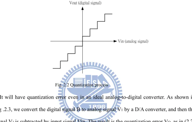
We can get a discrete-time signal by sampling a continuous-time signal, and this sampled signal can be converted to digital signal. Quantization will appear in this process, the basic concept of quantization is to classify the original signal to different levels according to its level to determine the bit number of this signal, as shown in Fig. 2.2.
Fig. 2.2 Quantization process
It will have quantization error even in an ideal analog-to-digital converter. As shown in Fig .2.3, we convert the digital signal B to analog signal V1 by a D/A converter, and then the
signal V1 is subtracted by input signal Vin. The result is the quantization error VQ, as in (2.2)
[18].
VQ=Vin–V1 (2.2)
Fig. 2.3 Quantization error caused by A/D converter
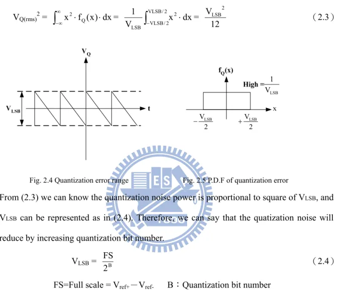
probability density function of quantization error is uniformly distributed between ±VLSB/2
and its mean is zero, as shown in Fig. 2.5. From this assumption, we can easily get the quantization noise power VQ(rms)2 in (2.3).
VQ(rms)2 =
∫
= ∞ ∞ − x ⋅fQ(x)⋅dx 2∫
− ⋅ 2 / VLSB 2 / VLSB 2 dx x V 1 LSB = 12 VLSB2 (2.3) 2 VLSB + 2 VLSB − LSB V 1Fig. 2.4 Quantization error range Fig. 2.5 P.D.F of quantization error
From (2.3) we can know the quantization noise power is proportional to square of VLSB, and
VLSB can be represented as in (2.4). Therefore, we can say that the quatization noise will
reduce by increasing quantization bit number. VLSB = B
2 FS
(2.4) FS=Full scale = Vref+-Vref- B:Quantization bit number
Assume that input signal is sinusoidal, expressed as Vin(t) = A sinωt, so the input signal
power Vin(rms)2 is as (2.5). In (2.5), we define the amplitude of input signal is the full scale
of reference voltage, and from (2.3), (2.4) and (2.5), the peak SNR(Peak Signal-to-Noise Ratio) can be derived as in (2.6).
Vin(rms)2 =
∫
− ⋅ ⋅ 2 / T 2 / T 2 dt ) t sin A ( T 1 ω = 2 A2 = 8 ) A 2 ( 2 = 8 FS2 (2.5) PSNR = 10 log( 2 ) rms ( Q 2 ) rms ( in V V )= 6.02B + 1.76 dB (2.6)additional bit number in quantizer increases 6dB in SNR. In Nyquist A/D converters, increasing the resolution of quantizer (decrease VLSB) while reducing the quantization noise is
a general method to reach higher SNR, but this method is sensitive to mismatches of analog device. Therefore, the general Nyquist A/D converter is not easily to implement with high resolution.
2.3 Techniques of Sigma-Delta Modulator
ΣΔ A/D converters are based on oversampling and noise shaping to reach high resolution. Oversampling means the sampling rate is much higher than Nyquist rate, about 8~512 times in general applications. The goal of oversampling is to expand quantization noise to wider range. It can reduce the quantization noise in signal bandwidth and increase the DR (Dynamic range) of input signal. Noise shaping is a technique that moves noise to high frequency, which is done by using discrete time filter and feedback technique. After noise shaping, the noise in high frequency can be filtered out by a digital filter [19].
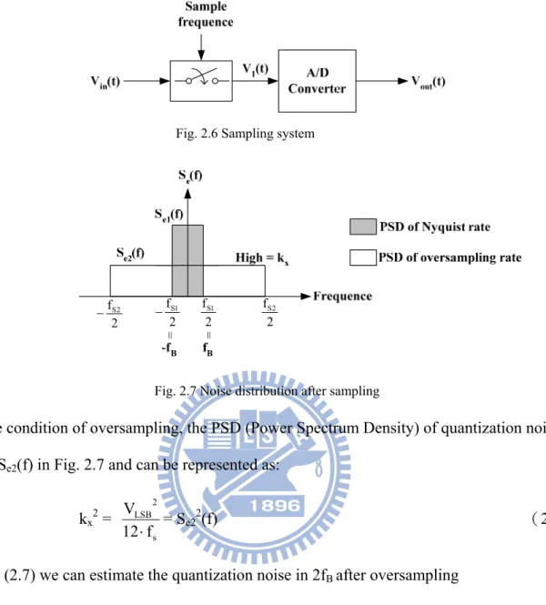
2.3.1 Oversampling Technique
First, we made the assumption that quantization noise is a uniform distribution in sampling spectrum so its mean is zero and is a white noise [20]. The system in Fig. 2.6 just has oversampling function and does not have noise shaping effect. If a A/D converter is sampled in Nyquist rate, then the quantization noise is uniform distributed between ±fB ; if it is
sampled by oversampling technique, then quantization noise is uniform distributed between± fS2/2s, which is much larger than fB. As shown in Fig. 2.7, if the signal bandwidth
is between ±fB, then quantization noise in this bandwidth will be reduced by using
Fig. 2.6 Sampling system 2 fS1 2 fS1 − 2 fS2 2 fS2 −
Fig. 2.7 Noise distribution after sampling
In the condition of oversampling, the PSD (Power Spectrum Density) of quantization noise is as Se2(f) in Fig. 2.7 and can be represented as:
kx2 = s 2 LSB f 12 V ⋅ = Se2 2(f) (2.7)
From (2.7) we can estimate the quantization noise in 2fB after oversampling
PQ =
∫
= − ⋅ B B f f 2 x df k OSR 2 12 FS 12 V f f 2 B 2 2 2 LSB s B ⋅ ⋅ = ⋅ (2.8)In (2.8), we define a parameter OSR (Oversampling Ratio) as OSR = B s f 2 f (2.9)
Finally, we can get PSNR from (2.5) and (2.8)
PSNR = 10 log( Q signal P P )= 6.02B + 1.76 + 10 log(OSR) (2.10)
From (2.10), we can find that doubling OSR will increase 3dB in PSNR, which is about 0.5 bit increase in resolution. Although oversampling can reduce quantization noise, it is
difficult to reach high SNR when using a low bit quantizer. For example, if we need a 16bit A/D converter, then SNR must be equal to 98dB, if the signal bandwidth is 20KHz, then the sampling rate must equal to 2 × 109 × 20KHz, it is impossible to implement. Because at such high frequency, quantization noise is no longer a white noise, it is correlated with input signal. So there is not only oversampling technique, we must add noise shaping technique also, if we want to achieve high resolution.
2.3.2 Noise Shaping
We can model a general ΣΔ modulator and its linear model as shown in Fig. 2.8.
H(z) Quantizer y(n) x(n) u(n) (a) (b)
Fig. 2.8 (a) General ΣΔ modulator (b) Linear model with quantization noise
From Fig. 2.8(a), we can derive output Y(z) as (2.11) Y(z) = ) z ( H 1 ) z ( H + X(z) + 1 H(z) 1 + E(z) (2.11) and define Signal Transfer Function STF and Noise transfer function NTF as
STF (z)= ) z ( H 1 ) z ( H ) z ( X ) z ( Y + = (2.12) NTF (z)= ) z ( H 1 1 ) z ( E ) z ( Y + = (2.13)
where H(z) is the transfer function of a discrete time filter. There have two important meanings in (2.12), (2.13). If we want to obtain highest SNR, STF must be equal to 1, that
means the input signal can transfer to output without attenuating; and NTF (z) must be equal
to 0, because the quantization noise will not affect output SNR.
In order to make NTF (z) be a high pass filter, so at DC(z = 1), NTF must be 0, and z = 1 is
a pole of H(z), so the transfer function H(z) of the discrete filter is as H(z) = 1 Z 1 − = 1 1 Z 1 Z − − − (2.14) Substitute (2.14) into (2.12) and (2.13), we can get
STF (z) = z 1 (2.15) NTF (z) = z 1 1− (2.16)
And we substitute z with fs f 2 j
e
π
, then we can plot STF(f)2 and NTF(f) 2 in frequency domain, as Fig. 2.9. We can find NTF(f)2 also increases with frequency, and STF(f)2 is always equal to 1, if we choose signal bandwidth in low frequency, then we can get highest signal power and lowest noise power, from this figure we see that quantization noise is moved to higher frequency significantly, this is the noise shaping effect.
2 TF(f) N 2 TF(f) S
Fig. 2.9 Noise shaping
After noise shaping, we can filter out the noise in high frequency by using digital filter, and we will illustrate its architecture more detail in the next chapter.
3
Architectures of Sigma-Delta Modulator
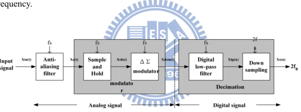
Before we introduce various architectures of ΣΔ modulators, we must to realize the basic architecture of a general A/D converter. Fig. 3.1 is a complete block diagram of a A/D converter [18], and we can divide it into two different parts. First part is the modulator. The main function of this part is doing oversampling and noise shaping to the input analog signal. Second part is the decimation filter. The main function of this part is to remove noise in high frequency and down sampling the sampling frequency to base band frequency.
ΣΔ ΣΔ
ΣΔ
Fig. 3.1 Block diagram of ΣΔ A/D converter
First, the input signal Xin(t) pass an Anti-aliasing filter, the 3dB frequency of this filter is about few times of Nyquist frequency, so signal and noise out of Nyquist frequency is filtered roughly, and this signal goes into the ΣΔ modulator after goes through a S/H circuit. However, in the circuits implement situation, the sample and hold function is included in the circuits of modulator, so the signal Xc(t) will pass this modulator and produces a high speed data code Xdsm(n), because of noise shaping, the quantization noise will appear in high frequency. Finally, we must filter the noise in high frequency and reduce the sampling frequency to Nyquist frequency by a decimator, and passes the digital signal to
the output [18].
In this chapter, we will focus on the architectures of ΣΔ modulator, because that the noise model and optimal method is focus on this part, we must understand the theorem, benefits and drawbacks of each kinds of ΣΔ modulators. In addition, the implement of decimator is very typical [21][22]. In today’s technology, DSP processors are also used to replace decimators, so we will introduce this part roughly.
3.1 First-Order Sigma-Delta Modulator
We recall that H(z) in (2.14) is 1 1 Z 1 Z − −
− , substitute it into Fig. 2.8, then we can get a first-order modulator; Analyze transfer function H(z) from time-domain, it indicates that output signal m(t) is obtained by adding the delayed input signal n(t-1) and the delayed output signal m(t-1), so we can express a complete first-order
ΣΔ
ΣΔ modulator as Fig. 3.2.
Fig. 3.2 First-order ΣΔ modulator
H(z) in Fig. 3.2 is indicated the effects of delay and accumulation, this is equivalent with
an integrator in circuit design, so the three circuits components of ΣΔ modulator are integrator, quantizer and DAC in the feedback path.
Y(z) = z-1X(z) + (1-z-1)E(z) (3.1) From (3.1) we can find the signal transfer function is as a delay function, and noise transfer function is as a high pass filter, moves the noise to high frequency. In order to derive PSNR of first order modulator, we must get the magnitude of NTF(z) and STF(z) in the
frequency domain, so we substitute z with , and get ΣΔ s f / f 2 j e π⋅ STF(f) and NTF(f) respectively as: 1 j2πf/fs TF(f) z e S = − = − ⋅ = 1 (3.2) NTF(f) = 1-e−j2π⋅f/fs= j f/fs s e j 2 ) f f sin(π × × −π⋅ ⇒ ( ) 2 sin( ) s TF f f f N = ⋅ π (3.3)
So the quantization noise in base band ±fB can obtain by (2.7) and (3.3)
df f f f V df f N f S P B B B B f f s s LSB TF f f e Q ⎥ ⋅ ⎦ ⎤ ⎢ ⎣ ⎡ ⎟⎟ ⎠ ⎞ ⎜⎜ ⎝ ⎛ ⋅ ⋅ = ⋅ =
∫
∫
− − 2 2 2 2 sin 2 12 ) ( ) ( π (3.4)Because that fB is much lower than fs, so sin(π f/fs) is approximate equal to (π f/fs), and PQ is
as PQ = 3 2 2 LSB ) OSR 1 ( 36 V ⋅ π = 2B 3 2 2 OSR 2 36 FS ⋅ ⋅ ⋅π (3.5) From (2.5) and (3.5), if we have the maximum signal power, then PSNR is as (3.6)
PSNR = 10 log( Q signal P P ) = 10 log( 22B 2 3 ) + 10 log[ 3 2 (OSR) 3 π ] = 6.02B + 1.76-5.17 + 30 log(OSR) (3.6) From (3.6), we find that each octave of OSR, PSNR will increase 9dB, increase 1.5 bit in resolution. Compare (3.6) with (2.10) that only has oversampling effect; we can find that 1st order noise shaping increases the performance of ΣΔ modulator.
3.2 Single-Loop Second-Order Sigma-Delta Modulator
When the discrete time filter in Fig. 2.8 is replaced by two cascade integrator, then it is a second order modulator, output of the first integrator is only connecting with the input of the second integrator, it is shown in Fig. 3.3
ΣΔ
Fig. 3.3 Single loop second order ΣΔ modulator
Then the output of it can easily be derived as
Y(z) = z-2X(z) + (1-z-1)2E(z) (3.7) where STF and NTF is as
STF(z) = z-2 (3.8)
NTF(z) = (1- z-1)2 (3.9)
Using the same method in (3.3) (3.4), we can obtain
STF(f) =1 (3.10) 2 s TF f f sin 2 ) f ( N ⎥ ⎦ ⎤ ⎢ ⎣ ⎡ ⎟⎟ ⎠ ⎞ ⎜⎜ ⎝ ⎛ ⋅ = π (3.11) PQ = 5 4 2 LSB OSR 60 V ⋅ ⋅π = 2B 2 4 5 OSR 60 2 FS ⋅ ⋅ ⋅π (3.12) So finally, PSNR of the second order ΣΔ modulator is as
PSNR = 10 log( Q signal P P ) = 10 log( 22B 2 3 ) + 10 log[ 5 4 (OSR) 5 π ]
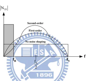
= 6.02B + 1.76-12.9 + 50 log(OSR) (3.13) In the single loop second order architecture, each octave of OSR can increase PSNR by 15 dB, it is equivalent to 2.5 bit in resolution. If we compare (3.13), (3.11) with NTF(f) =1 that without noise shaping, as Fig. 3.4, we can find that in our needed signal bandwidth, the quantization noise is highest when NTF(f) =1, and that with second order noise shaping is smallest among this figure [18].
TF N
2 fS
Fig. 3.4 Comparison of noise shaping techniques
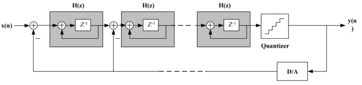
3.3 Single-Loop High Order Sigma-Delta Modulator
Fig. 3.5 is a single loop high order ΣΔ modulator, from the derivation in Section 3.1 and Section 3.2, we can get the quantization noise PQ in signal bandwidth is as
PQ = 2L 1 L 2 2 LSB ) OSR 1 ( 1 L 2 12 V ⋅ + + ⋅ π ,L:order (3.14) and its PSNR is PSNR = 6.02B+1.76-10 log( 1 L 2 L 2 + π )+(20L+10) log(OSR) (3.15) In the application of high order ΣΔ modulator, (6L+3)dB increases in SNR when OSR is octave, so PSNR can be raised by increasing the order of the system, especially at large oversampling ratio. But sometimes in high order architecture, the performance will be
worsen than result predicted by (3.13), because of the stability problem, it will make less effective noise shaping function, so the quantization noise will not be suppressed completely.
Fig 3.5 Single-loop high order ΣΔ modulator
3.4 Interpolative Sigma-Delta Modulator
Interpolative is a kind of high order ΣΔ modulator, it changes connection of some stages, adds some feedforward paths and feedback paths in order to suppose more aggressive noise shaping effect, Fig. 3.6 is a four-order interpolative architecture ΣΔ modulator [23]. 1 1 z 1 z − − − 1 1 z 1 z − − − 1 1 z 1 z − − − 1 1 z 1 z − − −
Fig. 3.6 Four-order interpolative architecture
This architecture also has stability problem, when the order L increases, each integrator produces one pole, and when the order is higher, poles of this system will also increase, and it will cause unstable situation, so the range of integrator gain will be limited; if the range of integrator gain is small, oscillation will appear in the circuits. Another is the considerations of clock control, when we use SC (switched-capacitor) to implement the integrator, each
integrator needs two clocks to control its operation, and we will need more clock to control the integrator when the order of system increases, it will produce more problems.
3.5 MASH Architecture
MASH (Multi-stage noise shaping) architecture is also called cascade architecture, which is a method that cascades several low order loops modulator in order to get high order noise shaping effect. The fundamental ideal of MASH is delivering quantization noise of front stage to input of next stage, and combining the digital outputs of all the stages with proper transfer function in digital domain, only the quantization noise of last stage will appear at the output, and the orders of NTF is the same with total orders in the cascade modulator.
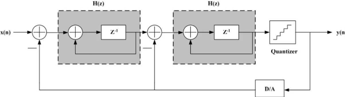
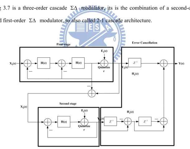
Fig 3.7 is a three-order cascade
ΣΔ
ΣΔ modulator, its is the combination of a second-order and first-order ΣΔ modulator, so also called 2-1 cascade architecture.
1 − Z 1 − Z Z−1
Fig. 3.7 2-1 architecture MASH ΣΔ modulator
From Fig. 3.7, we can derive the first stage output Y1(z) can be represented as
Y1(z) = z-2X1(z) + (1-z-1)2E1(z) (3.16)
Y2(z) = z-1X2(z) + (1-z-1)E2(z) (3.17)
and overall output of MASH Y(z) is as
Y(z) = H1(z)Y1(z) + H2(z)Y2(z) (3.18)
and we can say that second stage input X2(z) is almost the same with E1(z), in order to
eliminate first stage quantization noise E1(z), from (3.16) ~ (3.18), we can define the error
cancellation functions H1(z) and H2(z) as
H1(z) = z-1 (3.19)
H2(z) = (1-z-1)2 (3.20)
From (3.16)~(3.20), E1(z) can be eliminated, and second stage quantization noise E2(z) is
shaped by third-order noise shaping function, and the MASH output Y(z) is as
Y(z) = z-3X1(z) + (1-z-1)3E2(z) (3.21)
The most significant advantage of this architecture is that stability is not an issue, because it is composed by several low-order systems, and the quantization noise will not be amplified stage by stage, so its stability is good. Most important, the noise shaping function is equivalent as high order modulator, so it is popular in recent publications [4][6]. However, there also have some drawbacks of this topology; it is sensitive to the circuits' imperfections, such as finite DC gain of OTA, variance of integrator gain due to capacitor mismatch and non-zero switch resistance. These are all practical considerations when we design a MASH architecture modulator [3].
ΣΔ
ΣΔ
3.6 Multi-bit Quantizer Sigma-Delta Modulator
The demands of high resolution and high bandwidth ADC are more and more in recent years. In a high signal bandwidth, OSR of ΣΔ ADC can’t be too high, and the peak SNR of a modulator with such limited OSR can’t satisfy of high resolution applications, if we use higher order architecture, then the performance will degrade due to instability. So the most general method to increase performance is to use multibit quantizer. The most
obvious advantage of using multibit quantizer is that the distance between quantizer level VLSB in (2.4) is much smaller due to increasing of B, and according to (2.3), the power of
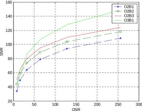
quantization noise is attenuated. Fig. 3.8 is the results of theoretical peak SNR of ΣΔ modulator versus oversampling ratio, with different order and quantizer bits, it is noted that peak SNR of the same OSR is increase 6 dB with each additional bit number in quantizer, and at low OSR, low order higher bit number architecture has equivalent performance as high order architecture. This result is usable for high bandwidth applications, and the power consumption of digital circuit in ΣΔ modulator is reduced due to lower sampling rate [24].
160 0 50 100 150 200 250 300 20 40 60 80 100 120 O2B1 O2B2 O2B3 O3B1 140 OSR S NR
Fig. 3.8 SNR vs. OSR with different quantizer bit number
Because of using multi-bit quantizer, so we also need to use multi-bit DAC(Digital-to Analog Converter) to transfer the digital output to analog signal, and feed it back to integrator. The most significant disadvantage is the non-linearities introduced by multi-bit DAC can degrade the performance of ΣΔ converter, like Fig. 3.9. It is a linear model of multi-bit modulator, where E(Q) and E(D) represent the quantization noise and feedback DAC noise respectively. The values of these capacitor elements in DAC will not equal to ideal values that we need, it is due to process variation, typical value of mismatch
in modern CMOS technology is about 0.05% ~ 0.5%. In recent years, so many researches are make efforts on reduce DAC noise due to mismatch, such as trimming [19], Dynamic element matching (DEM)[8][25], although trimming is effective, but it has a expensive production step. So, DEM becomes more and more popular because of its efficiency and cheaper cost.
Fig. 3.9 Multi-bit architecture
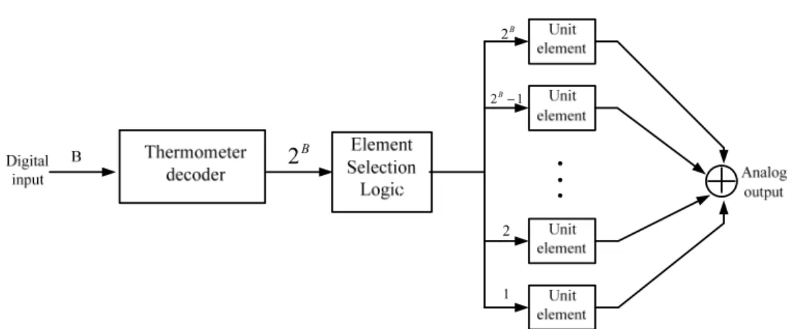
3.7 Multi-bit Sigma-Delta Modulator use DEM Technique
Dynamic element matching is a different approach to decrease the DAC noise, it is used to improve the linearity of pure DACs [26], but now it is most used in inner DAC of multi-bit modulator. A DAC with DEM technique is illustrated in Fig. 3.10, bits thermometer code is put into the element selection logic block, and the function of element selection logic is try to select DAC elements in such way let the errors introduced by DAC average to zero for several operation periods. Because the DEM block is located in feedback loop, so its delay must be very small prevent to degrade the performance of
ΣΔ 2B
ΣΔ converter, therefore the algorithm used in the DEM block must be simple. There are several techniques of DEM, such as Randomization [27], Clocked Averaging (CLA) [26], Individual Level Averaging (ILA) [28], Data Weighted Averaging (DWA) [29], Randomization is the first approach to use DEM technique in ADC, and DWA offers a good performance to reduce DAC error, in this section, an overview introduction of these two algorithms will be presented, and the operation
principle of them will be explained. 1 2B− 1 2 B 2 B 2
Fig. 3.10 A B-bit DAC with DEM technique
3.7.1
Randomization Technique
The main operation principle of randomization is that the element selection logic performs as a randomizer. In each clock period, the randomizer selects DAC elements randomly to generate the output of DAC. If the randomizer is ideal, then the DAC noise will become uncorrelated with each other. Simulation results show that randomization DEM technique reduces the noise floor from DAC error by several dB, but it still be a white noise in low frequency. Fig. 3.12 is the output spectrum of a second-order ΣΔ modulator with a 0.1% capacitor mismatch, it is notable that the noise floor of randomization DEM is lower than that without any calibration technique in the feedback DAC.
3.7.2
Data Weighted Averaging (DWA)
DWA is a efficiently method to reduce DAC mismatch noise, it uses one register to remember the capacitor last time used, and always points to the first unused unit capacitor in this clock, so DWA rotates through all the unit capacitors such that all capacitors are used at the maximum possible rate. From this algorithm, each elements is used the same number of times in long interval, this ensures that the errors caused by the DAC average to zero
quickly. In Fig. 3.11, it is a 4-bit DAC and the shaded boxes are the number of 1’s in the thermometer code. Assumes that the input codes sequence is 8, 8, 10, 9, 10, 10, 11, 11, 12, 11, 14, 11, 14, 13, 12, 15... Fig. 3.12 is the simulation results of a third order ΣΔ modulator, we can see that without DEM has highest noise floor and DWA works as a first order noise shaping function of DAC noise, ideal DAC only with quantization noise has third-order noise shaping.
Un it Ca p. Un it Ca p.
Fig. 3.11 Operation principle of the DWA algorithm
10-3 10-2 10-1 -200 -180 -160 -140 -120 -100 -80 -60 -40 -20 0 60 dB/decade PS D Normalized Frequency No DEM DWA ideal DAC
Fig. 3.12 Output spectrum with three kinds of DAC
Another consideration is the sub-ADC(quantizer) of the ΣΔ modulator, we usually use Flash A/D as the multi-bit quantizer because of its high speed, but Flash A/D has a significant disadvantage is that the number of comparators of it is proportional to 2B. That means a 6 bit quantizer needs 64 comparators, the occupied area of comparator may not much, but in modern SOC applications, the problems of power and area are important, so it becomes one limitation of multi-bit quantization.
ΣΔ A/D converter is attractive for high resolution application, for higher signal bandwidth, we increase system order to raise SNR, but it still have stability problem. So people develop MASH and multi-bit architecture to improve its performance. Finally, we classify they into low order, high order, MASH and multi-bit four kinds of architecture, and compare their advantage and disadvantage as Fig. 3.13 [30]
ΣΔ
Fig. 3.13 Comparison of ΣΔ modulator architectures
3.8 Decimator
In ΣΔ A/D converter, digital decimator is used to process digital signal of the quantizer output, the high speed data word after oversampling modulation can’t be used directly. Because there have original signal and quantization noise among it, so the main function of decimator is to convert the oversampled B-bit output words of the quantizer at a sampling rate of fs to N-bit words at Nyquist rate of input, and removes the noise out of signal band.
In order to prevent the noise introduced by other frequency, the decimator filter must have very flat signal pass-band, and sharp transition region and enough signal attenuation in stop band. Two-stage decimator is used in a general situation, because that single stage decimator is difficult to convert sampling rate to Nyquist rate in 1 time and without degrading SNR. In the first stage, we can down-sample the sample frequency to 2~4 times of Nyquist frequency, and in the second stage, we can use IIR or FIR filter that have high linearity [19]. For a large OSR, multi-stage decimator is used.
3.9 Performance Metrics for a
ΣΔModulator
In order to understand the performance merits used to specify the behavior of ΣΔ modulator, several specifications concerning the performance are discussed [15].
․Signal to Noise Ratio: The SNR of a data converter is the ratio of the signal power to the noise power, measured at the output of the converter for a certain input amplitude. The maximum SNR that a converter can achieve is called the peak SNR.
․Signal to Noise and Distortion Ratio: The SNDR of a converter is the ratio of the signal power to the power of the noise and the distortion components, measured at the output of the converter for a certain input amplitude. The maximum SNDR that a converter can achieve is called the peak SNDR.
․Dynamic Range at the input: The DRi is the ratio between the power of the largest
input signal that can be applied without significantly degrading the performance of the converter, and the power of the smallest detectable input signal. The level of significantly degrading the performance is defined as the point where the SNDR is 6 dB bellow the peak SNDR. The smallest detectable input signal is determined by the noise floor of the converter.
․Dynamic Range at the output: The dynamic range can also be considered at the output of the converter. The ratio between maximum and minimum output power is the dynamic
range at the output DRo, which is exactly equal to peak SNR.
․Effective Number of Bits: ENOB gives an indication of how many bits would be
required in an ideal quantizer to get the same performance as the converter. This numbers also includes the distortion components and can be calculated from (2.6) as 02 . 6 76 . 1 ENOB= SNR− (3.22) ․Overload Level: OL is defined as the relative input amplitude where the SNDR is
decreased by 6dB compared to peak SNDR
Typically, these specifications are reported using plots like Fig. 3.14. This figure shows the SNR and SNDR of the converter versus the amplitude of the sinusoidal wave applied to the input of the converter. For small input levels, the distortion components are submerged in the noise floor of the converter. Consequently, the SNDR and SNR curves coincide for small input levels. When the input level increases, the distortion components start to degrade the modulator performance. Therefore, the SNDR will be smaller than the SNR for large input signals. Note that these specifications are dependent on the frequency of the input signal and the clock frequency of the converter. Fig. 3.14 also shows that SNDR curves drop very fast once the overload point is achieved. This is due to the overloading effect of the quantizer which results in instabilities.
ΣΔ
4
Discuss About Different Architecture of
Non-idealities Noise and Distortion Models
Proposing an optimization algorithm for searching design parameters which maximizes ΣΔ
ADC SNDR, while minimizing power consumption is one of the primary purposes. Model completeness determines success of this goal. The ΣΔ modulator major nonidealities are finite OTA gain error, thermal noise, settling error, multi-bit DAC noise, and jitter noise. All nonideality models in our model are expressed in noise power forms.
Our model can include all SDM typical architectures where all noises are dominated by the first integrator in the chain. And some noises or distortion (quantization noise [30], finite gain error [30], settling error [9] and nonlinear DC-gain distortion [31]) may change in different system structure which related to order number or system feedback value see as Fig. 4.1. Furthermore, thermal noise [30], multi-bit DAC noise [32], jitter noise [1] and DAC distortion are independent of system architecture.
5
Op-amp Non-Linear Gain Curve
5.1 DC-gain Distortion Can Be Severe
A second order SDM with OSR = 20, = 0.6, a 3-bit quantizer, a 1V sinusoidal input
signal, and a relatively small DC-gain = 50db, will see a severe DC-Gain distortion at about -61dB, which easily dominates other noises and distortions, e.g. quantization noise (-81 dB) and DAC distortion (-76 dB, without DEM), and results in a poor SNDR at 60 dB.
OS V
O
A
5.2 Modeling Nonlinear DC-gain Curves
It is well known that the output resistance of op-amp output-stage-transistors is dependent on the output voltage . This dependency results in nonlinear op-amp
DC-gain when changes, as is shown in Fig. 5.1. A typical nonlinear DC-gain curve can be approximated by the polynomial:
O V O V ) 1 ( ) ( 4 4 2 2 0 o o o V V A qV qV A = + + (5.1) where is the nonlinear DC-gain of op-amp, and is the maximum DC-gain when
is in the neighborhood of 0V. ) ( o V V A AO O V
It is well known that VGSQ of the output-stage transistors and the maximum DC-gain
are the only two parameters which can affect the shape of the nonlinear curves . It is
also well known that maximum output swing and
O A ) ( o V V A OS
V VGSQ have germane relation with
each other. Since VOS makes much more sense for practical designers, we replace VGSQ by
, and in the rest of this paper and are the only two parameters which affect
OS
) ( o
V V
A . In order to demonstrate the effects of and on , Spice op-amp
simulations in Fig. 5.2(a), (b) respectively show the effects that and can have on the shape of DC-gain curves.
OS
V AO AV(Vo)
O
A VOS
Fig. 5.1 DCG curve versus output voltage with the rail to rail voltage of VDD
(a) (b)
Fig. 5.2 (a) Two nonlinear DC-gain curves with identical VOS but different
O
A
O
A
(b) Two nonlinear DC-gain curves with similar but different VOS
In order to model the nonlinear gain , we tried various combination of and
to create a set of representative curves for the family of nonlinear DC-gain curves.
) ( o V V A AO OS V V V A0 =570 , OS =1 V V A0 =321 , OS =1 A0 =321 ,VOS =1V A0 =331 ,VOS =1.6V
Then, we endeavored to find out suitable and such that (5.1) can reasonably fit
all of these curves. After intensive tries and errors, we come up with the and in (5.1) to be 2 q q4 2 q q4 q ≡ −9⋅( AO0.01 )2 6 . 2 2 (5.2) (1+VOS) 4 83 . 0 0001 . 0 ) ( 6⋅ AO − ≡ (5.3) 4 ) 1 ( V q + OS
Although the and are obtained from tries and errors, the searching and testing time for them is more than one year. We are confident that the model (5.1) – (5.3) is sufficiently general and accurate, as is verified in the next subsection.
2
q q4
5.3 Verifying Nonlinear DC-Gain Curve Model
Comparisons of DC-gain curves from real op-amps and from our model (5.1) – (5.3) are shown in Fig. 5.3. The comparisons are
Real op-amp Our model
-0.3595
q2 =-0.067,q4 =
Maximum error is 380(≈5%)
Two stage op-amp
V V
A0 =10180 OS =1.5
Real op-amp Our model
q2 =-0.124,q4 =-0.335
Maximum error is 70(≈2%)
Folded cascode op-amp
V V A0 =3184 OS =1.43 (b) Real op-amp Our model -0.883 q 0.565, - 4 2 = = q Maximum error is 130(≈2%) Two stage op-amp
V V A0 = 6819 OS = 0.8 (c) Real op-amp Our model q2 =-0.0916,q4 =-0.2967 Maximum error is 20(≈0.1%)
Folded cascode op-amp
V V
A0 = 6849 OS =1.5
(d)
deliberately planed to cover various op-amp structures and representative points in op-amp parameter space. The sub-figures in Fig. 5.3 are cross-related as follows:
1. (a) and (c) are two-stage op-amps, and (b) and (d) are folded cascode op-amps. 2. (a) and (b) have large difference in the values of A . O
3. (c) and (d) differs mainly in VOS .
For the four cases presented in Fig. 5.3, the errors between op-amp nonlinear DC-gain curves from real op-amps and from our model range from 0.1% to 5%. This demonstrates that our model (5.1) – (5.3) is sufficiently general and accurate.
6
SDM DISTORTION DUE TO THE
NONLINEAR DC-GAIN OF THE
OPERATIONAL AMPLIFIER
In section 6, we analyze the op-amp nonlinear DC-gain phenomenon, and obtain a nonlinear DC-gain model (5.1) – (5.3). In this section, based on the model (5.1) – (5.3), we want to derive a nonlinear distortion model for all architecture SDM output distortions caused by nonlinear DC-gain in op-amps. Fig.6.1 shows the block diagram of an ideal SDM for single-loop 2nd. We will first discuss the property of which is the input to the first integrator. Then the transfer characteristics of the integrator are analyzed, based on which the SDM nonlinear DC-gain distortion model is derived. Distortion models for other SDM structures can be obtained following the approach in this section.
S
V
Fig. 6.1 Single-loop second-order ΣΔ modulator
6.1 Properties of V
SIn Fig. 6.1, the SC integrator input VS can be expressed without the noise part as
) ( ) 1 ( ) (z z X z V norder S − − = (6.1)
) sin( )
(n A wnT
x = in , we perform inverse z-transform to (6.1), and one obtains
) cos( ) sin( sin( ) ( n A wnT A nT V in in S ⋅ ≈ ) ) ( ( ) ) ( sin( ) wnT OSR T n n w u T n n w A order order order in ⋅ × −
π
= − ⋅ − (6.2) Then, the amplitude of VS can be approximated as(6.3) A w T n wnT n A nT n V
AVS = S( order ⋅ ) = insin( order⋅ ) ≅ order⋅ in⋅ ⋅
6.2 Transfer Characteristics of the First Integrator
The sampling phase and integration phase of a switch capacitor integrator are shown in Fig. 6.2. In the following discussion, signals VO((n+1/2)T) , VO((n−1/2)T) and will be respectively denoted by , and . Suppose settling problem is ignored, which requires separate treatment. Then, the sampling phase is ideal, and the input/output characteristics of the integration phase can be completely described by the following three equations ) (nT Vs + O V VO− VS
(a) Sampling phase (b) integration phase Fig. 6.2 Switch-capacitor integrator with nonlinear DC-gain op-amp
(6.4) (6.5) ) 1 ( ) ( O O 2 O2 4 O4 V V A qV qV A = + + ± ± ± =− ⋅ a O V O A V V V ( ) S S a o I a S a o V C V C V V C V V − − ⋅ = ⋅ − + ⋅ ⋅( + +) + ( − −) I C (6.6)
} 1 )] ) ( ) ( ) ( ) ( ) ( ) ( ) ( ) (( ) ( ) ) ( ) )( ( ) (( [ 1 1 { 4 3 1 2 2 1 3 4 2 2 4 2 2 2 S O O O O O O O O O O O O O O S O O V A V V V V V V V V q q V V V V q A K V V ⋅ + + + + + ⋅ − + + + ⋅ ⋅ + ⋅ = − ∞ − − + − + − + + − − + + − + L (6.7) where KS is I S C
C . The problem with (6.7) is that the integrator output
also appears at right-hand-side of (6.7). However, since can be shown to relate to in (6.2) as follows ± O V V ± O V S } ) 2 1 ( sin { 2 sin 4 4 1 1 1 ⎟ ⎠ ⎞ ⎜ ⎝ ⎛ ± ⋅ ⋅ ⋅ ⋅ − ⋅ + + − ≈ ± A w n T wT A K A K K V VS O S O S S O (6.8)
the and at right-hand side of (6.7) can be substituted by (6.8) and (6.2), and take its nonlinear term resulting in
± O V VS (6.9)
{
sin( ) sin( ( ) ) (( ) )}
)} ( cos ) ( 1 1 ) 4 4 ( 1 ) ( sin ) ( cos ) 5708 . 1 ( cot ) ( 1 1 ) 4 4 ( 10 ) ( sin ) 5708 . 1 ( cot ) ( 1 1 ) 4 4 ( 5 ) ( sin ) 5708 . 1 ( cot 1 1 4 4 3 { 1 4 2 2 4 4 4 2 2 2 2 2 2 4 4 4 2 4 4 2 2 4 4 4 2 2 2 2 2 2 T n n u T n n w A wnT A wnT q q A A K A K wnT wnT OSR q q A A K A K wnT OSR q q A A K K A K wnT OSR q A A K K A K A K V V order order in in VS O S O S VS O S O S VS O S S O S VS O S S O s O S O O − ⋅ − − ⋅ ⋅ − ⋅ ⋅ ⎟ ⎟ ⎟ ⎟ ⎠ ⎞ ⎜ ⎜ ⎜ ⎜ ⎝ ⎛ + ⋅ − + ⋅ ⋅ ⋅ − ⋅ ⋅ ⎟ ⎟ ⎟ ⎟ ⎠ ⎞ ⎜ ⎜ ⎜ ⎜ ⎝ ⎛ + ⋅ − + ⋅ ⋅ − ⋅ ⋅ ⎟⎟ ⎟ ⎟ ⎟ ⎠ ⎞ ⎜⎜ ⎜ ⎜ ⎜ ⎝ ⎛ + + ⋅ − + ⋅ ⋅ ⋅ ⋅ ⎟⎟ ⎟ ⎟ ⎟ ⎠ ⎞ ⎜⎜ ⎜ ⎜ ⎜ ⎝ ⎛ + + ⋅ − ⋅ = − − +Equation (6.9) can be used to compute nonlinear DC-gain distortions appearing at 1st integrator output.
6.3 Nonlinear DC-gain Distortions at SDM Output
It is known that if the gain of the behind integrator equals one, i.e. CS2/CI2 = 1,the same distortions appearing at 1st integrator output would appear at SDM output. Otherwise, some modification is needed on distortions at SDM output. Suppose behind integrator gain equals one. Then, the 3rd harmonic magnitudes in DC-gain disotritons can be computed from (6.9) as follows ⎥⎦ ⎤ ⎢⎣ ⎡ − ⋅ ⋅ − ⋅ ⋅ ⋅ + + ⋅ − + ⋅ − + ⋅ − − + ⋅ ⋅ ⋅ + + ⋅ − + ⋅ − − ⋅ ⋅ ⋅ = ) cos( 1 )} ( ] 1 1 [ ] ) 4 4 ( 3 ) 5708 . 1 ( cot ) 4 4 ( 10 ) 5708 . 1 ( cot ) 4 4 ( 25 [ ] 1 1 [ ] 4 4 4 ) 5708 . 1 ( cot 4 4 12 {[ 16 1 1 2 2 4 4 4 0 2 2 2 4 2 2 2 2 0 2 3 sin_ OSR n q q A A A K K A K OSR A K OSR A K q A A A K K A K OSR A K A K A order in VS S S O S O S O S in VS S S O S O S O S π (6.10) ⎥⎦ ⎤ ⎢⎣ ⎡ ⋅ ⋅ − ⋅ ⋅ ⋅ + + ⋅ − + ⋅ − ⋅ − − + ⋅ ⋅ ⋅ + + ⋅ − ⋅ − − ⋅ ⋅ ⋅ = ) sin( )} ( ] 1 1 [ ] ) 4 4 ( 5 ) 5708 . 1 ( cot ) 4 4 ( 10 ) 5708 . 1 ( cot ) 4 4 ( 15 [ ] 1 1 [ ] ) 4 4 ( 4 ) 5708 . 1 ( cot ) 4 4 ( 12 {[ 16 1 1 2 2 4 4 4 0 2 2 2 4 2 2 2 2 0 2 2 2 3 cos_ OSR n q q A A A K K A K OSR A K -OSR A K q A A A K K A K -OSR A K A K A order in VS S S O S O S O S in VS S S O S O S O S π (6.11)
⎥⎦ ⎤ ⎢⎣ ⎡ − ⋅ ⋅ − ⋅ ⋅ ⋅ + + ⋅ − + ⋅ − − ⋅ − ⋅ ⋅ ⋅ = ) ( cos 1 )} ( ] 1 1 [ ] ) 4 4 ( 1 ) 5708 . 1 ( cot ) 4 4 ( 10 ) 5708 . 1 ( cot ) 4 4 ( 5 {[ 16 1 1 A 2 2 4 4 4 0 2 2 2 4 2 5 sin_ OSR n q q A A A K K Ao K OSR Ao K OSR Ao K A K order in vs s s s s s O s π (6.12) ) ( sin } ) ( ] 1 1 [ ] ) 4 4 ( 1 ) 5708 . 1 ( ) 4 4 ( 10 ) 5708 . 1 ( ) 4 4 ( 5 {[ 16 1 1 A 2 2 4 4 4 0 2 2 2 4 2 5 cos_ OSR n q q A A A K Ao K OSR Cot Ao K OSR Cot Ao K A K order in vs s s s s O s π ⋅ ⋅ − ⋅ ⋅ ⋅ + ⋅ − + ⋅ − − ⋅ − ⋅ ⋅ ⋅ = (6.13) Then the powers of the 3rd and 5th harmonic distortions are
2 ) ( log 10 ) ( 3 2 3 cos_ 2 3 sin_ A A dB HD NFDCG = + (6.14) 2 ) ( log 10 ) ( 5 2 5 cos_ 2 5 sin_ A A dB HD NFDCG + =
(6.15)
The model (6.10)-(6.15) indicates that the DC-gain distortions at SDM output are related to , , , , and OSR. Some qualitative properties about how each parameter can affect distortion magnitude are obtained from (6.10)-(6.15) and listed in TABLE 6.1.
I
C
C
S Ain AO VOS I C ↑ C ↑S Ain↑ A ↑ O VOS↑ OSR↑ Distortion magnitude ↓ ↑ ↑ ↓ ↓ ↓Some quantitative investigation based on (6.10)-(6.15) shows that and OSR are the most influential parameters on SDM DC-gain distortions. Therefore, an interesting example about how (6.10)-(6.15) can be utilized is that if the four parameters are fixed at = 1v,
= 0.8, = 1pF and = 2pF , then (6.10)-(6.15) can be employed to determine the minimum and OSR required so that the DC-gain distortion can be kept under certain value. The results of single-loop 2nd are tabulated in TABLE 6.2.
O A in A OS V S C O A I C HD3 distortion power(dB) HD5 distortion power(dB) AO OSR -70 -80 ≧1000 ≧16 -90 -100 ≧3000 ≧64 -110 -120 ≧6400 ≧256
TABLE 6.2 Minimum requiredAO and OSR
Due to loop shaping, the DC-gain nonlinearity in the second integrator degrades the
performance to a much lesser extent, allowing a more relaxed design [33]. Therefore, only the DC-gain distortion caused by first integrator is considered in this paper.
6.4 Behaving Model Simulation Results
We use a calculable behavior model to verify our SDM nonlinear DC-gain distortion model. The z-domain transfer function of a delayed integrator of sigma-delta modulator is
1 1 1 ) ( − − ⋅ − ⋅ = z z g z H α (6.16) ) 1 ( 1 1 0 2 0 0 2 0