國 立 交 通 大 學
電機學院 電信學程
碩士論文
直序式超寬頻無線射頻接收機之CMOS帶陷可調式
低雜訊放大器設計與研究
Design of CMOS Tunable Band-notch Low-noise Amplifier for
DS-UWB Wireless RF Receiver
研究生:蔡柏瑤
指導教授:周復芳 博士
直序式超寬頻無線射頻接收機之CMOS帶陷可調式
低雜訊放大器設計與研究
Design of CMOS Tunable Low-noise Amplifier for
DS-UWB Wireless RF Receiver
研究生:蔡柏瑤
Student: Po-Yao Tsai
指導教授:周復芳 博士 Advisor: Dr. Christina F. Jou
國 立 交 通 大 學
電機學院 電信學程
碩 士 論 文
A Thesis
Submitted to College of Electrical and Computer Engineering
National Chiao Tung University
in partial Fulfillment of the Requirements
for the Degree of
Master of Science
in
Communication Engineering
June 2009
Hsinchu, Taiwan, Republic of China
直序式超寬頻無線射頻接收機之CMOS帶陷可調式
低雜訊放大器設計與研究
學生: 蔡 柏瑤
指導教授: 周 復芳
國立交通大學
電機學院
電信學程碩士班
摘
要
本論文研製之帶陷式低雜訊放大器是應用在直序式超寬頻(DS-UWB)的系統 上。電路的設計主要是藉由實驗室內的完成電路 (Notch LNA),加上壓控電容, 在 UWB 的頻帶內達到頻率可調的效果。
在超寬頻(Ultra Wide Band) 的工作頻帶(3.1 ~ 10.6GHz)內,除了 DS-UWB 的訊號外,尚有 IEEE 802.11a 的 WLAN 信號存在於 5~6GHz 的頻帶內,這些訊號的 存在會與 DS-UWB 的訊號產生交互調變失真(Inter-modulation distortion),進 而干擾到 DS-UWB 的訊號。因此,直序式超寬頻調變技術在定義其工作頻帶時, 刻意避開了 5~6G 的頻帶,達到降低信號干擾的目地。電路架構上是先以兩個電 感所形成的 Transformer feedback,做第一級的輸入匹配,達到寬頻匹配與雜 訊抑制的效果,再於第一級的放大器後方加上一可調式帶陷濾波器,用來衰減干 擾訊號(5~6GHz),接著再串一級放大器來提高增益。當中,為了降低功率損耗, 每一級的放大器都只用單一電晶體去完成,而非 Cascode 的架構,因而,此電路 的直流偏壓只需要一伏特。最後,將 LNA 串接源極隨耦器(source follower)完 成寬頻輸出阻抗匹配。此寬頻低雜訊放大器模擬結果如下:頻寬為 3 ~ 10 GHz, 平均增益為 11dB,雜訊指數為 2 ~ 4 dB,輸入反射係數小於 10 dB,input P1dB
Design of CMOS Tunable Low-noise Amplifier for
DS-UWB Wireless RF Receiver
Student: Po-Yao Tsai Advisors: Dr. Christina F. Jou
Degree Program of Electrical and Computer Engineering
National Chiao Tung University
ABSTRACT
A procedure is the design and analysis of a band notch low-noise amplifier applied in the receiver of DS-UWB. The design in this thesis is based on a finished circuit “Notch LNA” and then makes it tunable in virtue of the adding varactor.
The signal within the operation band of UWB (3.1 ~ 10.6GHz), includes not only the signal of DS-UWB but the WLAN signal of IEEE 802.11a (5~ 6GHz). These undesired signals will cause inter-modulation and hence interfere with the signal of DS-UWB. Thus, the operation band of DS-UWB doesn’t include 5~6 GHz to prevent interference. About circuit architecture in this thesis, transformer feedback is the first stage for getting broadband input matching and low noise contribution. Tunable notch
filter is inserted in back of the first transistor, and then cascade another transistor to increase gain. For getting lower power consumption, we use single transistor in each stage so the applied voltage of amplifiers just 1 volt only. Finally, this LNA series with a source follower for output matching.The simulation results are as follows:
The bandwidth is 3 ~ 10 GHz. The average gain is 12 dB. The noise figure is 2 ~ 4 dB. The input return loss is lower than 10dB. The input P1dB(min.) is -24dBm. The
誌 謝
電子產業中,絕大多數的產業技能都可透過自修或公司內的教育
訓練來學習,唯獨 IC 設計,門檻特高,若在學校沒有接觸過,便很
難有機會在業界從事相關的工作,為此,感謝我的指導教授周 復芳
博士,讓我有機會進到 919 實驗室,得以接觸到 RFIC 的設計。
論文研究期間,曾試過幾個題目,如 Frequency Tripler、Tunable
duplexer、Broadband amplifier 等,以及最後的 Tunable band notch
LNA,在這段時間,有幾度因失敗感到沮喪,甚至心灰意冷,主因是
論文研究不同於課堂上的課業,無法保證你所投入的心力是可以成比
例回收的,對此,由衷感謝博班學長吳 匯儀,若非您的鼓勵與指導,
我可能早已放棄學業。
最後,感謝百忙之中撥空前來參與口試的評審委員 李 信宏教授
與胡 樹一 教授,讓我有機會能在這學期順利完成學業。
CONTENTS
Chinese Abstract
I
English Abstract
II
Acknowledgement
IV
Contents
V
List of Tables
VI
List of Figures
VII
Chapter 1 Introduction... - 1 -
1.1 Background and motivation... - 1 -
1.2 Thesis organizations... - 3 -
Chapter 2 Tunable CMOS Band-notch LNA
...
- 4 -
2.1 Input matching... - 4 -
.Transformer feedback... 6
-2.2 Notch filter... - 8 -
.Tunable notch filter... 8
-2.3 UWB LNA Review... - 12 -
2.4 Circuit implement... - 15 -
2.5 Simulation result... - 18 -
Chapter 3 Improvement... -26-
3.1 Circuit analysis ... - 27 -
3.2 Simulation result ... - 28 -
Chapter 4 Conclusion and future work...-30-
4.1 Conclusion... - 30 -
4.2 Future work... - 32 -
List of Tables
Table 1.1 Time-Frequency Codes (TFC)...3
Table 2.1 TT Corner post-simulation summary...18
Table 2.2 SS Corner post-simulation summary ...20
Table 2.3 FF Corner post-simulation summary ...22
Table 2.4 Comparison of Ultra Wide-band LNA...24
List of Figures
Fig. 1.1 DS-UWB spectrum allocation...1
Fig. 1.2 MB-OFDM UWB allocation...2
Fig. 2.1 The general topologies for 1
ststage of LNA ...4
Fig. 2.2 Transformer feedback...7
Fig. 2.3 Notch filter topologies...8
Fig. 2.4 Proposed notch filter...9
Fig. 2.5 Band notch response...9
Fig. 2.6 The spectrum of band notch filter with ideal LC components....10
Fig. 2.7 Tunable notch filter ...10
Fig. 2.8 The spectrum of tunable band notch filter...11
Fig. 2.9 Common-gate cascade common-source stage noise circuit ...12
Fig. 2.10 A common-source amplifier with bridged-shunt peaking ...12
Fig. 2.11 Topology of the proposed UWB LNA ...13
Fig. 2.12 LNA small signal diagram ...13
Fig. 2.13 Input port equivalent circuit ...14
Fig. 2.14 Band notch LNA ...15
Fig. 2.15 Tunable band notch LNA ...17
Fig. 2.16 TT corner simulation result ...18
Fig. 2.17 SS corner simulation result ...20
Fig. 2.18 FF corner simulation result …...22
Fig. 3.1 WLAN signals allocation...25
Fig. 3.2 Improved circuit structure...26
Fig. 3.3 SS corner simulation result...27
Fig. 4.1 Tunable notch filter with topology of inductive degeneration ...30
Fig. 4.2 Return loss and gain flatness ………...31
Chapter 1 Introduction
1.1 Background and motivation
Ultra-wide-band (UWB) systems is an advanced indoor wireless technology capable of transmitting data over a wide spectrum of frequency bands with very low power and high data rates within 5 to 10 meters transmitted range. Its operation frequency range is from 3.1GHz to 10.6GHz which was announced by Federal Communications Commission (FCC) in 2002.
The definitions of UWB:
1. Any signal whose fractional bandwidth is equal to or greater than 20% of the center frequency.
2. The occupied bandwidth of signal equals to or greater than 500MHz. In UWB systems, there are two major modulation technologies for use:
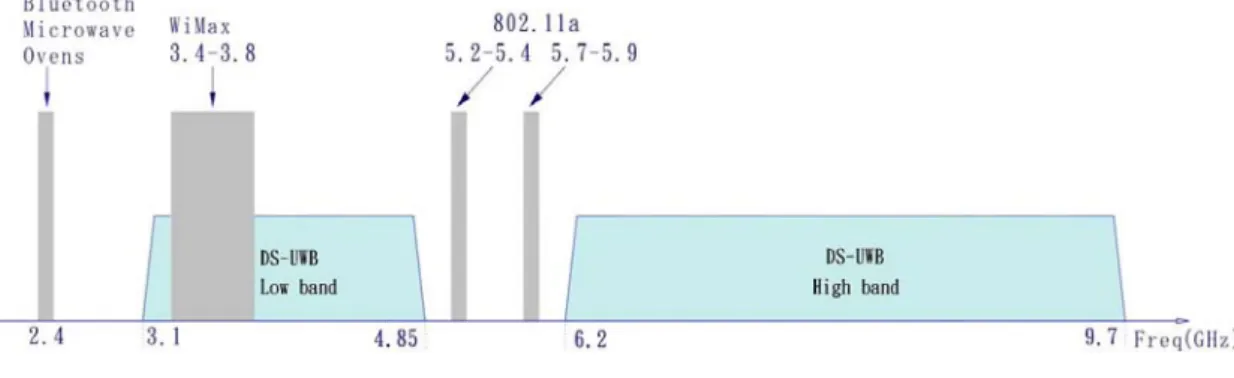
1) Direct-sequence UWB (DS-UWB):
It supports data communication using both BPSK and 4-BOK. The BPSK is mandatory and 4-BOK modulation is optional. BPSK modulation is low complexity and easy to implement. Every compliant device will be able to both transmit and receive BPSK modulated signals. DS-UWB supports two independent bands of operation. Fig.1.1, shows the reference spectral mask for DS-UWB scheme. The lower band occupies the spectrum from 3.1-4.85GHz and the upper band occupies the spectrum from 6.2-9.7GHz. The 5-6GHz band is dedicated to WLAN 802.11a systems.
Fig. 1.1 DS-UWB allocation
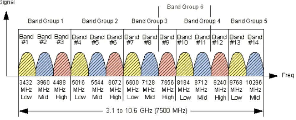
2) Multi-band orthogonal frequency division multiplexing UWB (MB-OFDM UWB) proposal:
In Multi-Band-OFDM (MB-OFDM) UWB, frequency span is grouped into 5 major Band Groups which are in turn sub-divided into 14 bands in total, as shown in Fig. 1.2. Each band is 528MHz bandwidth, and the center frequency of each band is m×264 MHz, where m is from 13 to 39.
Fig. 1.2 MB-OFDM UWB allocation
The parameter that determines the hopping sequence of the six OFDM symbol bursts is the Time-Frequency Code (TFC). For example, the hopping sequence for TFC 1 in Band Group 1 is Band 1-2-3-1-2-3. Band Groups 2 - 4 and Band Group 6 follow the same sequences using their respective bands. Band Group 5 only hops between two bands and thus has it's own sequence.
Time-Frequency Codes (TFC)
TFC Band
group Band Hopping Sequence
1 1 2 3 1 2 3 2 1 3 2 1 3 2 3 1 1 2 2 3 3 4 1 1 3 3 2 2 5 1 1 1 1 1 1 6 2 2 2 2 2 2 7 3 3 3 3 3 3 8 1 2 1 2 1 2 9 1 3 1 3 1 3 10 1 2 3 2 3 2 3
Band Groups 2 to 4 and Band Group 6 follow the same sequences using their respective bands
5 13 13 13 13 13 13
6 14 14 14 14 14 14
8
5
13 14 13 14 13 14
Table 1.1 Time-Frequency Codes (TFC)
Data rates of UWB:
The UWB system provides a wireless PAN with data payload communication capabilities of 53.3, 55, 80, 106.67, 110, 160, 200,320, and 480 Mb/s.
MB-OFDM uses a total of 122 sub-carriers that are modulated using quadrature phase shift keying (QPSK).Forward error correction coding (convolutional coding) is used with a coding rate of 1/2,1/3,3/4,5/8,11/32.
Table 1.2 MB-OFDM Data Rate Parameters
1.2 Thesis organization
This thesis discusses about the circuit design and implementation of Band-notch Low-Noise Amplifier for UWB. In chapter 2, we will review diverse topologies of notch LNA, and present our design with simulated results in TSMC 0.18 μm CMOS process. Finally, an improved circuit will be discussed in chapter 3, and then make a conclusion in chapter 4.
MB-OFDM Data Rate Parameters
Data Rate
(Mb/sec) Modulation Type Coding Rate
53.3 QPSK 1/3 80 QPSK 1/2 106.7 QPSK 1/3 160 QPSK 1/2 200 QPSK 5/8 320 DCM 1/2 400 DCM 5/8 480 DCM 3/4
Chapter 2
Tunable CMOS Band-notch LNA
Low-noise amplifier (LNA) is a critical device since it’s typically the first stage in receiver. The common goals in design are:
1. Low noise figure (NF) 2. Sufficient linearity
3. Input and output matching 4. Low power consumption. 5. Gain flatness
6. Stability
2.1 The general topologies of 1
ststage in LNA
In a communication system, in order to make LNA connect to an antenna, the first problem facing is wide-band input matching.
The general topologies of 1st stage in LNA are shown in Fig. 2.1
(a) Resistive termination (b) Shunt-series feedback
(c) 1/gmtermination (d) Inductive degeneration
1. Resistive termination
Adding a 50ohm resistor to the input node of a common source amplifier, as shown in Fig. 2.1 (a). Such topology is rarely used in the LNA design since the real resistor will contribute noise and cause an unacceptable high noise figure. But the noise contribution of the terminating resistors can be neglected when an antenna is mounted directly on the amplifier.
2. Shunt-series feedback
A LNA with the shunt-series feedback topology as Fig. 2.1(b), often have high power dissipation. The cause is the bias point of input fastened with the output voltage, and hence the biasing point of system can’t be set at the optimal bias point.
In addition, the shunt series feedback topology has a stability problem in high frequency. The root cause is related to source resistance Rs, it can’t be negative, or the system will oscillate. But the parasitic component of transistor can’t be neglected in high frequency so the feedback effect would make the stability of system drop to unstable region.
3. 1/g
mtermination
This topology seems like a good choice for wide bandwidth system because the transistor’s gm is merely affected in the frequency range of UWB system. In order to
make 1/ gm equal to 50Ω, gm has to be fixed at 20mS. This means the transistor size
must be fixed, and it will affect the noise figure of system. Rather than other topologies, the gain of such LNA is rarely small. Therefore, there will be more than one stage in back of this topology for enhancing the overall gain.
In common gate configuration, the noise figure and matching circuits totally depend on the transistor. The (2.1) shows the noise factor of the single transistor [1].
α γ
+ = 1
F (2.1)
where γ is the coefficient of channel thermal noise and α is
0 d m g g = α (2.2)
where gm is the trans-conductance and g is the zero-bias drain conductance. d0
For the long channel device, γ equals to 2/3 and α equals to 1. For the short channel device, the value of γ is greater than 2/3. Based on these data, the best noise figure of this topology tends to be more than 2.2dB.
Consequently, this topology can afford quite wide bandwidth impedance matching but bring a large noise figure and is difficult to achieve high gain performance.
4. Inductive degeneration
From the small signal model shown as Fig. 2.2(b), the input impedance of this architecture can be calculated as
s gs m gs g s in L C g SC L L s Z = ( + )+ 1 +( ) (2.3)
At the resonant frequency, the input impedance is purely real and proportional to Ls. Therefore, this system don’t have to add additional any resistive components and it
can reach the input impedance matching by choosing appropriate value of the Ls. This
leads to a very good noise figure and impedance matching for a narrow bandwidth system.
However, since this topology utilizes resonance at the desired frequency, it can be used only for narrow bandwidth signals and it is not suitable for wide bandwidth applications.
Transformer feedback
Transformer feedback is the commendable topology of input matching, and it has been reported in [2], as shown in Fig. 2.2. The causes are its noise contribution (refer to T1 in Fig. 2.2) in transformer winds is relatively small, and the response of an
on-chip transformer can allow the realization of an absolutely stable band-pass feedback network. Moreover, such topology can replace the multi-inductor network to get broadband input matching, and hence the additional noise and more chip area due to multi-inductor will be prevented. By the way, the input impedance with feedback is determined by the effective turns ratio of T1 (n/k) and the trans-conductance (gm) of
Fig. 2.2 Transformer feedback
According to (2.4), the 3dB bandwidth of transformer is limited by the magnetic coupling (k) between windings. Thus, we can get k ≧ 0.6 is required for full bandwidth of UWB. l u l u f f f f k + − ≥ (2.4)
The high-k transformer design is good for reducing the pass band attenuation. The highest magnetic coupling can achieve in virtue of overlaying transformer windings. Such technology has another advance that the chip can hence be save more.[3]
Note that the bandwidth defined by (2.4) does not account for capacitive parasites which impair the higher-frequency response. The limitation of bandwidth caused by inter-winding capacitance will be mitigated by using the transformer in the inverting configuration where each winding has one terminal at AC ground.
The trans-conductance of Q1 defines the input stage loop gain and is selected in conjunction with the effective turns ratio (i.e., n/k ~ 5.25) of T1. The magnetizing inductance of T1 matches the input impedance to 50Ω and provides a noise figure less than 3dB at the lower edge of the amplifier pass-band.
2.2 Notch filter
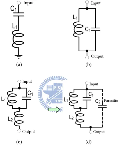
The notch filter is a filter that passes all frequencies except those in a stop band centered on a center frequency. Here, Fig. 2.3 (a) and (b), show the general two LC tanks of notch filter. Fig. 2.3 (c) is part of the proposed topologies of notch filter in this thesis.
(a) (b)
(c) (d) Fig. 2.3 Notch filter topologies
Fig. 2.3 (d), shows the notch filter of Fig. 2.3 (c) with the parasitic capacitor from transistor. Its impedance is given by (2.5), and the series resonance frequency is
1 2 1|| ) ( 2 / 1 π L L C . [4] 1 )] ( [ ) || 1 )( ( ) ( 2 2 2 1 1 1 2 1 2 1 2 2 1 2 1 2 2 1 + + + + + + = C L C L C L C C L L s s C L L s L L s s Z (2.5)
Tunable notch filter
Fig. 2.4 shows the proposed notch filter composed of Fig.2.3 (b) and (c). Rather than narrowband rejection of WLAN signal, we aim at filtering out all WLAN signals (i.e. 5.1-5.9GHz), as show in Fig. 2.5
Fig. 2.4 Proposed notch filter
Fig. 2.5 Band notch response
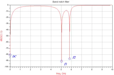
The notch filter 1 in Fig. 2.3, is a simple parallel circuit and its resonant frequency is given by (2.6). At its resonant frequency, the input signal will be rejected so we’ll see a notch frequency f1,as marked in Fig. 2.5.
1 2 3 2 1 2 1 f C L LC f = = = π π (2.6)
The notch filter 2 in Fig. 2.3, tends to be a simple series circuit at high frequency. As the tank tends to be resonant at f2, its low impedance will short the signal to
ground, thus there is a notch point in Fig. 2.6. Additionally, the notch filter 2 tends to be a parallel circuit at low frequency, which is set to equal to f1. In virtue of such
topology, we can get the wide band rejection nature as shown in Fig. 2.3.5. Finally, we use varactor to fulfill tunable function, as show in Fig 2.8.
There is some confusion when it comes to the derivations of the resonant frequencies of the notch filter, hence the derivations of the relevant equations for the filter is also included later.
Fig. 2.6 The spectrum of band notch filter with ideal LC components
(a) Tuning voltage = 0V (b) Tuning voltage = 1V Fig. 2.8 The spectrum of tunable band notch filter
Related equation derivation:
1 ) ( 1 ) ( 1 ) 1 || ( ) ( 1 1 22 1 1 2 1 2 1 1 2 1 2 1 2 3 1 2 1 1 2 1 2 1 1 1 + + + = + + + = + + = + = C L S L L C L L S S C L S SL C L L S SL SL C L S SL SL SC SL S Z ∞ = ) ( 1 S Z when S2L1C1+1=0 1 1 2 1 C L f π = (Parallel resonant) (2.7) 0 ) ( 1 S = Z when: 1. S =0 f=0=DC 2. 02 1 2 1+ 1+ 2 = L L C L L S 1 2 1 2 1 2 C L L L L S =− + 2 1 2 1 2 1 2 1 f C L L L L f = + = π (Series resonant) (2.8)
2.3 UWB LNA Review
In this section, we’ll discuss some diverse topologies of UWB LNA. Then, the characteristic of our design will be indicated in next section.
Fig. 2.9
Fig. 2.9 shows a LNA structure in [5], fabricated in 0.13um2 CMOS process, using cascode configuration and without notch characteristic. Cascode configuration is a typical technology in high gain, and broadband amplifier design since it can reduce the effective input capacitor and increase the output loading. In addition, the cascode structure also has good properties of reverse isolation and such characteristic is useful for broadband matching. However, it’s not good to noise figure due to the noise contribution from trans-conductance of additional transistor.
(a) (b) Fig. 2.11
Fig. 2.11 shows a notch LNA structure in [6], fabricated in 0.35um2 SiGe BiCMOS technology ,consisting of the cascode configuration, active notch filter, and emitter follower. The notch filter sketched in Fig. 2.11(b) is reported in [7]. It synthesizes impedance that combines a series resonance, at frequency
] ) || ( 2 /[
1 π L3 C3 +C4 Cvar , and with a parallel one , at frequency 1/(2π L3C4||Cvar).
When the frequency is at series resonant frequency, the input impedance of the notch filter will greatly deteriorate the voltage gain of the LNA, thus the rejection of WLAN signal is obtained, which can be manipulated by the varactor.
(a) Spectrum (b) Tuning result Fig. 2.12
(a) (b)
(c) Fig 2.13
Fig. 2.13 shows another notch LNA structure in [4], fabricated in 0.13um2 CMOS process, using passive LC tanks to achieve the notch characteristic. Such LC tank, which will be elaborated later, has not only a series resonance but a parallel resonance. However, its gain flatness isn’t good enough, as shown in Fig 2.13 (c).
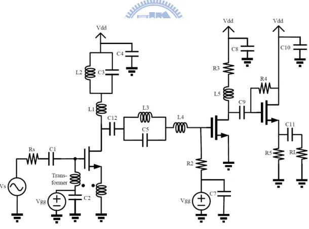
2.4 Circuit implement
There are four core topologies in this thesis as list below: 1. Transformer feedback for input matching
2. Tunable notch filter for wide band rejection with tuning function 3. Cascade topology for gain improvement
4. Source follower for output matching
Furthermore, the design in this thesis is based on a finished circuit “Notch LNA” in our lab and then makes it tunable in virtue of the adding varactor.
The prototypes and layouts of both “Notch LNA” and “Tunable band notch
LNA” are shown in Fig. 2.14 and Fig. 2.15.
``
Fig. 2.14(b) The layout of band notch LNA
2.5 Simulation result
In this section, the measured results are shown below.
1. TT corner
Freq. range (GHz) 3~10 S11(dB) <-8 S22(dB) <-8 S21(dB) 12 S12(dB) <-50 NF(dB) 2.4~3.2 5GHz Notch(dB) -8 Power(mW) 15.8 P1dB(dBm) -24 IIP3(dBm) -3Table 2.1 TT Corner post-simulation summary
Fig. 2.16 (b) Noise Figure under TT corner
Fig. 2.16 (c) P1dB under TT corner
Fig. 2.16 (e) Stability under TT corner
2. SS corner
Freq. range (GHz) 3~10 S11(dB) <-8 S22(dB) <-9 S21(dB) 10 S12(dB) <-50 NF(dB) 2.7~3.5 5GHz Notch (dB) -8 Power(mw) 15.8 P1dB (dBm) -24 IIP3 (dBm) -0.5Table 2.2 SS Corner post-simulation summary
Fig. 2.17 (b) N.F under SS corner
Fig. 2.17 (c) P1dB under SS corner
Fig. 2.17 (e) stability under SS corner
3.FF corner
Freq range(GHz) 3~10 S11(dB) <-7 S22(dB) <-7 S21(dB) 13 S12(dB) <-50 NF(dB) 2.3~3.2 5GHz Notch(dB) -10 Power(mW) 15.8 P1dB(dBm) -24 IIP3(dB) -5Table 2.3 FF Corner post-simulation summary
Fig. 2.18 (b) N.F under SS corner
Fig. 2.18 (c) P1dB under SS corner
Fig. 2.18 (e) Stability
Comparison of UWB LNA
Spec. This work [8] [9] [10] [4] (Front end) [6] (Front end) Tech 0.18u CMOS 0.18u CMOS 0.18u CMOS 0.18u CMOS 0.18u CMOS 0.35u SiGe BiCMOS S11 (dB) <-11 <-8 <-10 <-11 <-8 <-7 Supply V 1 1.8 1.5 1.5 1.8 1.8 Gain (dB) 11 9.2 10.8~12 13.7~16.5 20 15 S12 (dB) <-55 -35 - <-30 - - NF 3~3.5 3.1~6 4.3~5.3 4.7~5.6 5.2~7.7 5~11 BW 3 ~10 3.1~10.6 3.1~10.6 3.1~10.6 3~8 3~8 Pdiss (mw) 15.8 11.9 4.5 10.6 18 49 Area 0.85 mm2 1.2 mm 2 1.0 mm2 0.66 mm2 1.7 mm2 3.57 mm2 5.1-5.9GHz notch (dB) -8 dB - - - Narrow Band notch: -10 dB Narrow Band notch: -8 dB P1dB(dBm) -21.6 - - -24 -12 -16 ~ -11
Chapter 3 Improvement
In previous design, the band notch LNA generates a flatness response in stop band to reject the WLAN signal of IEEE 802.11a in 5 to 6GHz. However, we found there was other WLAN applications exist in the band group2 as shown in Fig. 3.1, it is the HipLAN2 of ETSI.
Moreover, we also concern the interference from GSM signal since its power is relative strong to UWB. Hence, we make an improvement in previous design regarding these considerations and the circuit as show in Fig. 3.2.
Fig. 3.1 WLAN signals allocation
Stand Area Low Band (GHz) High Band(GHz) IEEE 802.11a North America 5.15-5.35 5.725-5.825 ETSI HiperLAN2 Europe 5.15-5.35 5.47-5.725 MMAC HiSWANa Japan 4.9-5.0 5.15-5.25
3.1 Circuit analysis
In this improvement, the core what we modify are adding one more notch filter (C13 L8) and tee type matching circuit. The additional notch filter is used to reject the GSM signal (1.8GHz to 1.9GHz), and the tee type matching circuit is added to help lowering S11 of the LNA.
3.2 Simulation result
Freq range(GHz) 3~10 S11(dB) < -10 S22(dB) <-10 S21(dB) 12 S12(dB) <-50 NF(dB) 3.3~3.9 5GHz Notch(dB) < -8 Power (mW) 31.5 P1dB (dBm) -24 IIP3(dB) -5Table 3.2 SS Corner pre-simulation summary
Fig. 3.3 (b) N.F under SS corner
Fig. 3.3 (c) N.F under SS corner
Chapter 4 Conclusion and future work
4.1 Conclusion
This thesis presents two tunable band notch UWB LNA’s based on the finished circuit “Notch LNA”. One is to reject the WLAN (5.1-5.9GHz) interference and another one is with the additional rejection aimed at GSM signal (1.8G ~1.9GHz). According to the simulated results, the feasibility of such band notch technique is confirmed.
In addition, we’ll also discuss another topology, such as Fig 4.1. The major difference is the placement of primary winding of transformer. According to its simulation result, we can know the noise figure and gain flatness will get better, but the return loss is hard to cover full band. The root causes are:
Fig. 4.1 Tunable notch filter with topology of inductive degeneration
1. Both of the inductance and size of primary winding are decrease. So the noise figure can get better.
2. The placement of transformer is similar to the topology shown in Fig 2.1(d), which is jut suitable for the device with narrow bandwidth but without mutual inductance.
Fig. 4.2 Return loss and gain flatness
4.2 Future Work
In this thesis, we have finished the design of UWB LNA’s. However, in ultra wide-band receiver architecture, there are still many important blocks needed to be implemented, such as Mixer, Synthesizer, etc. Besides forgoing, the ESD protection must be designed within the thinner gate oxide process. Finally, the EM EDA tool must be used accurately and all parasitic effects including parasitic capacitance, resistance and inductance must be considered carefully.
Reference
[1] Shaeffer, D.K.; Lee, T.H., “A 1.5-V, 1.5-GHz CMOS low noise amplifier”, Solid-State Circuits, IEEE Journal of Volume 32, Issue 5, pp.745 – 759, May 1997 [2] Michael T. Reiha, and John R. Long, “A 1.2 V Reactive-Feedback 3.1–10.6 GHz Low-Noise Amplifier in 0.13 um CMOS,” IEEE J. Solid-State Circuits, vol. 42, no. 5, May. 2007.
[3] J.R. Long, “Monolithic transformers for silicon RF IC design”, IEEE J.
Solid-State Circuits, vol. 35, pp. 1368-1382, Sept. 2000
[4] Giuseppe Cusmai, Massimo Brandolini, Paolo Rossi, and Francesco Svelto, ” A 0.18-_m CMOS Selective Receiver Front-End for UWB Applications,” IEEE J.
Solid-State Circuits, vol. 41, no. 8, Aug. 2006.
[5]Giang D. Nguyen, Kurt Cimino, and Milton Feng“A RF CMOS Amplifier with Optimized Gain, Noise, Linearity and Return Losses for UWB Applications,” [6] Andrea Bevilacqua, Andrea Maniero, Andrea Gerosa, and Andrea Neviani, ”An Integrated Solution for Suppressing WLAN Signals in UWB Receivers,” IEEE Trans.
Circuits and Syst.—I: Regular Papers, vol. 54, no. 8, Aug. 2007.
[7]T. H. Lee, H. Samavati, and H. R. Rategh, “5-GHz CMOS wireless LANs,” IEEE
Trans. Microw. Theory Tech., vol. 50, no. 1, pp. 268–280, Jan. 2002.
[8] Yi-Jing Lin, Shawn S. H. Hsu, Jun-De Jin, and C. Y. Chan, “A 3.1–10.6 GHz Ultra-Wideband CMOS Low Noise Amplifier With Current-Reused Technique,”
IEEE MWCL, March, 2007.
[9] S. Shekhar, X. Li, and D. J. Allstot, “A CMOS 3.1–10.6 GHz UWB LNA employing stagger-compensated series peaking,” Proc. IEEE RFIC Symp., San Francisco, CA, Jun. 2007, pp. 63–66.
[10] C.-T. Fu and C.-N. Kuo, “3–11-GHz CMOS UWB LNA using dual feedback for broadband matching,” Proc. IEEE RFIC Symp., San Francisco, CA, Jun. 2007, pp. 67–70.


![Fig. 2.9 shows a LNA structure in [5], fabricated in 0.13um 2 CMOS process, using cascode configuration and without notch characteristic](https://thumb-ap.123doks.com/thumbv2/9libinfo/8619856.191427/21.892.139.810.822.1072/shows-structure-fabricated-cmos-process-cascode-configuration-characteristic.webp)
![Fig. 2.11 shows a notch LNA structure in [6], fabricated in 0.35um 2 SiGe BiCMOS technology ,consisting of the cascode configuration, active notch filter, and emitter follower](https://thumb-ap.123doks.com/thumbv2/9libinfo/8619856.191427/22.892.139.757.167.460/structure-fabricated-bicmos-technology-consisting-cascode-configuration-follower.webp)
![Fig. 2.13 shows another notch LNA structure in [4], fabricated in 0.13um 2 CMOS process, using passive LC tanks to achieve the notch characteristic](https://thumb-ap.123doks.com/thumbv2/9libinfo/8619856.191427/23.892.138.750.115.738/shows-notch-structure-fabricated-process-passive-achieve-characteristic.webp)