國
立
交
通
大
學
電子工程學系 電子研究所
碩
士
論
文
於鍺基板製作n
+-p型二極體及n型金氧半
場效電晶體之電性研究
Electrical characteristics of n
+-p junction and
nMOSFETs on bulk Germanium
研 究 生:林敬倫
指導教授:簡昭欣 博士
於鍺基板製作n
+-p型二極體及n型金氧半
場效電晶體之電性研究
Electrical characteristics of n
+-p junction and
nMOSFETs on bulk Germanium
研 究 生:林敬倫 Student:Ching-Lun Lin
指導教授:簡昭欣 博士 Advisor:Dr. Chao-Hsin Chien
國 立 交 通 大 學
電子工程學系 電子研究所碩士班
碩 士 論 文
A Thesis
Submitted to Department of Electronics Engineering
and Institute of Electronics
College of Electrical and Computer Engineering
National Chiao Tung University
In Partial Fulfillment of the Requirements
For the Degree of Master
in
Electronics Engineering
September 2008
Hsinchu, Taiwan, Republic of China
於鍺基板製作n
+-p型二極體及n型金氧半
場效電晶體之電性研究
學生:林敬倫 指導教授
:簡昭欣 博士
國 立 交 通 大 學
電子工程學系 電子研究所 碩士班
摘 要
我們已經最佳化出在鍺基板上製作n+ -p型二極體的熱製程,並且進一步地成功製造 出在鍺基板上的n型金氧半場效電晶體。在我們一開始的二極體研究中,我們在光罩上 設計不同大小的離子佈值區域之面積去觀察二極體的漏電路徑。藉由總漏電流為「面積 漏電」(JA)和「邊界漏電」(JP)兩者所組成的觀念,我們可以定性地了解在對某種製程下 的漏電,究竟是被「面積漏電」亦或是「邊界漏電」的分量所主導。除此之外,對於面 積漏電和邊界漏電的定量萃取,也展現出和定性上所得的結果有一致的結論,並且我們 發現,無論是否在活化前沉積一層SiO2,沿著離子佈值區域的邊長上之缺陷應該被消除 掉,否則將會因嚴重的邊長漏電而導致反向漏電流的增加。然而,即使是這些缺陷被消 除的非常好,邊長漏電對於總漏電的比例還是和我們離子佈值區域的大小有關。因此, 當我們微縮電晶體的時候,這些沿著源極和汲極(S/D)的邊長分布之缺陷應該要被活化更 好。另一方面,我們發現活化前所沉積的SiO2層的作用是減少Al和Ge間的接觸電阻。因此,較高的順偏電流和較好的汲極飽和電流(drain saturation current)可以被達成。 藉由利用前面所得的活化製程最佳化的結果,我們接下來以高介電參數之介電層
Al2O3為閘極介電層,去製作出以鍺為基板的n型金氧半場效電晶體,並進一步地研究它
們的電性。無論是汲極電流對閘極電壓(Id-Vg)、汲極電流對汲極電壓(Id-Vd)和電容對電
壓(C-V)的特性,或者是一些電性參數,如:源極和汲極的電阻(source-drain resistance)、 載子內擴散長度(dopant in-diffusion length)和次臨界擺幅(sub-threshold swing)也被萃取 出來以了解元件的特性。雖然我們可以達到開關電流比(on-off ratio)對於汲極電流和源極 電流分別為 103和 104,但是嚴重的源極和汲極的電阻仍被觀察到。 最後,我們考慮使用氮氫混合氣體退火(FGA)製程去改善高電阻的缺點。一些參數 被萃取出來比較經過氮氫混合氣體退火前後的差異。結果顯示無論是源極和汲極的電阻 或者通道電阻(channel resistance)皆可被改善很多。不幸地,二極體接面漏電變得難 以控制並且大幅劣化我們的場效電晶體特性。確切的原因應該藉由進一步的物理分析來 證實。
Electrical characteristics of n
+-p junction and
nMOSFETs on bulk Germanium
Student:Ching-Lun Lin Advisors:Dr.
Chao-Hsin Chien
Department of Electronics Engineering and Institute of Electronics
National Chiao Tung University
ABSTRACT
We had optimized the thermal processes to form n+-p junction on bulk Germanium and further succeeded in fabricating Ge nMOSFETs. At the beginning of our diode studies, we designed different areas of implantation region on our masks to observe the leakage paths. By the concept which states total junction leakage currents were composed of JA and JP, we could know that the leakage current for certain fabrication process was dominated by “area” or “perimeter” component qualitatively. Besides, an quantitative extraction of JA and JP also consisted with these qualitative results, and we found no matter if a capping layer SiO2 was deposited before annealing, it exhibited defects along the perimeter of implantation region should be eliminated well, or an increasing reverse current would appear due to a severe JP. However, the ratio of perimeter current to total leakage current was still dependent on the dimension of our implantation area even if the defects were activated very well. Hence, as shrinking the transistors, the defects along the perimeter of S/D should be activated better. In
addition, we found the influence of capping layer SiO2 which was deposited just before
activation was to reduce the contact resistance between Al and Ge. Accordingly, a higher forward current and a much improvement on drain saturation current could be achieved.
By utilizing the results of optimization of the activation processes, we subsequently fabricated Ge nMOSFETs with Al2O3 as our high-k gate dielectric and further investigated their electrical performances. Not only Id-Vg, Id-Vd, and C-V performances, but also some electrical parameters, such as source-drain resistance, dopant in-diffusion length, and
sub-threshold swing, were extracted to realize the device characteristics. Although we could achieve on-off ratios about 103 and 104 for drain and source currents, respectively, a severe source-drain resistance was also observed.
Finally, we considered the forming gas annealing (FGA) process to improve the drawback. Some parameters were also extracted to compare together before and after FGA. It actually demonstrated not only source-drain resistance but also channel resistance could be much improved. Unfortunately, the junction leakage current became out of control and much degraded the electrical performances on our Ge nMOSFETs. The exact cause should be investigated by some further physical analysis.
致 謝
在兩年多的碩士生涯裡,我由衷地感謝指導教授 簡昭欣博士勞心勞力地幫我們實 驗室成員規劃了良好的學習環境,還帶我們去逛花市買花,替實驗室增添了許多生氣, 並且盡可能地提供我們每月的零用金。當然,對於我的碩士論文題目,老師也給予許多 專業的知識以及指導,讓我得到許多啟發,最終得以順利完成研究。更重要的是,老師 也多次的給予一些經驗,教導我們待人處世的道理。此外也萬分感謝 NDL 研究員 羅 廣禮博士,不厭其煩地協助我解決在實驗上的許多問題,若是沒有您的幫忙,論文中將 有許多部分難以完成。然而比較遺憾的是,當初我不清楚對於共同研究指導上,必須辦 理一些行政上的手續,因此雖然 羅廣禮博士實是我的共同指導,卻無法將您的大名掛 在論文封面,對於這樣的結果我感到萬分抱歉!於此,我再次的感謝 簡昭欣老師以及 羅廣禮博士! 對於我實驗的成果,有很大的部份要感謝 張俊彥老師團隊裡的鄭兆欽學長!每次 和您討論實驗數據,都著實讓我有相當多的收穫以及啟發。不論是多小的細節,或者是 我感到疑惑的任何地方,甚至是我沒注意到的事情,您都不厭其煩,甚至更進一步地分 析給我聽,讓我除了在問題上得到解答以及建議,也讓我看到了您帶學弟的風範,謝謝! 也非常感謝實驗室中的每一位學長以及同學,陪伴了我這兩年的研究生涯。楊明瑞 學長、沈志彥學長以及張家豪學長,謝謝你們在我有疑惑的時候,和我討論並給我許多 經驗和建議。帥氣幽默又搞笑的劉峻丞學長,非常謝謝你對我的激勵以及關心,並時常 給予我中肯的建議。詹効諭同學,謝謝你教我如何操作量測儀器、使用 Sigma Plot 以及 打網球;江欣哲同學,感謝你和我分享許多經驗,並時常幫忙我完成部份的實驗,也謝 謝你讓我見識到了一個人對籃球的執著,以及要如何挑戰自己的肝指數極限,而時常熬 夜做實驗;陳弘森同學,謝謝你每次幫我做的 ALD 步驟,也謝謝你開車載我和効諭, 帶我們走陸橋中央的奇妙經歷;陳宣凱吉祥物之叮噹貓,謝謝你教我們下圍棋,帶領我們徹夜找大鋼瓶,及讓我們知道雷射筆的厲害,也祝你實驗上苦盡甘來,一帆風順;郭 宇彥同學,謝謝你每次和我討論,都給予我不同切入問題的角度;陳猛飛同學,謝謝你 職場的經驗分享,以及實驗上的幫忙,也祝你工作上順順利利;楊登偉同學,謝謝你那 幾個晚上陪我做實驗,另外讓我們見識到 feel 來會發生什麼事,也祝你職場順利。也謝 謝實驗室中的各位可愛的學弟,朱柏錡、黃耀陞、許文朋、韓宗佑以及鐘政庭,陪伴我 渡過這段時光。另外也謝謝熱心且認真的黃菘宏同學,多次陪伴我做實驗,並當下給予 我許多建議及經驗,也祝你博士班順利畢業;羅老師實驗室的黃國洲、陸冠文同學,也 謝謝你們不辭辛勞的 train 我機台!以及許許多多未列出而曾經陪伴著我這兩年時光的 各位,謝謝! 最後,感謝我的爸媽,無怨無悔地對家庭的經營以及付出,讓我沒有後顧之憂,能 不斷的向前邁進,也謝謝弟弟為我打氣,謝謝你們! 林敬倫 於 新竹國立交通大學 2008 年 9 月
Contents
Abstract (Chinese) --- i
Abstract (English) --- iii
Acknowledgments --- v Contents --- vii Table Captions --- x Figure Captions --- xi
Chapter 1
Introduction
1-1 General Background --- 1 1-2 Motivation --- 41-3 Organization of This Thesis --- 6
Chapter 2
Optimization of bulk Germanium n
+-p junction
2-1 Introduction --- 102-2 Experimental Procedures --- 12
2-3 Results and Discussion --- 13
2-3-1 n+-p junction formation on bulk Ge with different activation temperatures -- 13
2-3-3 The effect of different implantation energies and activation times on the electrical characteristics of diodes --- 19 2-4 Summary --- 22
Chapter 3
The electrical performances of Germanium nMOSFETs with
various conditions of source/drain junction formation
3-1 Introduction --- 47 3-2 Experimental Procedures --- 49 3-3 Results and Discussion --- 51
3-3-1 Electrical characteristics of Ge nMOSFETs with various implantation and activation conditions --- 51 3-3-2 The effect of reducing thermal budget during activation on electrical
characteristics of the Ge nMOSFETs --- 53 3-4 Summary --- 56
Chapter 4
nMOSFETs on bulk Ge with forming gas annealing (FGA)
4-1 Introduction --- 70 4-2 Experimental Procedures --- 71 4-3 Results and Discussion --- 73
(FGA) --- 73
4-3-2 The interface quality and reliability of gate dielectric Al2O3 --- 75
4-4 Summary --- 76
Chapter 5
Conclusions and Suggestions for Future Work
5-1 Conclusions --- 885-2 Suggestions for Future work --- 90
References
--- 93Table Captions
Chapter 1
Table 1-1 ITRS 2007 Process Integration, Devices, and Structures
(High-Performance Logic Technology Requirements—Near-term) --- 8
Table 1-2 Some material parameters of semiconductors at room temperature --- 9
Chapter 2
Figure Captions
Chapter 1
Fig. 1-1 Energy band gap and band alignment of some high-K dielecrics relative to Si
--- 9
Chapter 2
Fig. 2-1 n+-p junction fabrication flow chart --- 23
Fig. 2-2 (a) The JA-V performances of diodes activated at 500 to 700℃ for 30sec. (b)
and (c) are the measurement of SIMS and Rs, respectively. Note the samples
are not capped SiO2 before annealing. --- 24
Fig. 2-3 It shows the fitting line of activation at 700℃ (solid curve) and an estimated
activation level after annealing at 500℃ (green dashed line). Note the
samples are not capped SiO2 before annealing. --- 25
Fig. 2-4 This picture illustrates the paths of junction leakage currents. The box-shaped
is the implantation region of Phosphorus with a perimeter of a. The dashed line is the edge of space charge region, and defects inside will contribute to a
drift leakage current. We separated the current into two main parts, JA and JP.
--- 25
Fig. 2-5 (a) The I-V characteristics of junctions activated at 500℃ for 30sec with
various dimensions. (b) and (c) show the JA-V and JP-V characteristics,
respectively. It hints the “perimeter current” dominates the leakage current
samples are not capped SiO2 before annealing. --- 26
Fig. 2-6 (a) The I-V characteristics of junctions activated at 600℃ for 30sec with
various dimensions. (b) and (c) show the JA-V and JP-V characteristics,
respectively. It hints the “perimeter current” dominates the leakage current
qualitatively. (d) It shows the extracted JA and JP quantitatively. Note the
samples are not capped SiO2 before annealing. --- 27
Fig. 2-7 (a) The I-V characteristics of junctions activated at 700℃ for 30sec with
various dimensions. (b) and (c) show the JA-V and JP-V characteristics,
respectively. It hints the “area current” dominates the leakage current
qualitatively. (d) It shows the extracted JA and JP quantitatively. Note the
samples are not capped SiO2 before annealing. --- 28
Fig. 2-8 (a) The comparison of the leakage current at various activation temperatures.
It is plotted by combining Fig. 2-5(d), Fig. 2-6(d), and Fig. 2-7(d) together. (b)
The extracted JP from (a) decreases with the increasing activation
temperature. --- 29
Fig. 2-9 (a) It exhibits the JA-V performances of diodes activated with or without
capping layer SiO2. (b) and (c) are the measurement of SIMS and Rs,
respectively. --- 30
Fig. 2-10 (a) The test structure is utilized to extract the contact resistance. The upper
and lower pictures are the profile and top view of this structure. (Z = 100 um, d = 160um) (b) The I-V characteristics of the test structure with or without
capping layer. (c) The extracted total resistance from (b) and calculated Rc are
plotted together. --- 31
Fig. 2-11 (a) The JA-V performances of diodes activated at 600 to 700℃ for 30sec. Note
the samples are capped SiO2 before annealing. (b) It is the measurement of Rs.
the samples are not capped SiO2 before annealing. --- 32
Fig. 2-12 The extracted total resistance and calculated contact resistance are plotted
together. The details of those labels are shown in Table. 2-1. --- 33
Fig. 2-13 (a) and (b) are the profiles of SIMS for samples with and w/o capping SiO2
before annealing, respectively. Samples in (a) are activated at 600 or 700℃
for 30sec. Samples in (b) are activated at 500 or 700℃ for 30sec. --- 34
Fig. 2-14 (a) The I-V characteristics of junctions activated at 600℃ for 30sec with
various dimensions. (b) and (c) show the JA-V and JP-V characteristics,
respectively. It hints the “perimeter current” dominates the leakage current
qualitatively. (d) It shows the extracted JA and JP quantitatively. Note the
samples are capped SiO2 before annealing. --- 35
Fig. 2-15 (a) The I-V characteristics of junctions activated at 650℃ for 30sec with
various dimensions. (b) and (c) show the JA-V and JP-V characteristics,
respectively. It hints the “area current” dominates the leakage current
qualitatively. (d) It shows the extracted JA and JP quantitatively. Note the .
samples are capped SiO2 before annealing. --- 36
Fig. 2-16 (a) The I-V characteristics of junctions activated at 700℃ for 30sec with
various dimensions. (b) and (c) show the JA-V and JP-V characteristics,
respectively. It hints the “area current” dominates the leakage current
qualitatively. (d) It shows the extracted JA and JP quantitatively. Note the
samples are capped SiO2 before annealing. --- 37
Fig. 2-17 (a) The comparison of the leakage current at various activation temperatures.
It is plotted by combining Fig. 2-14(d), Fig. 2-15(d), and Fig. 2-16(d) together.
(b) The extracted JP and JA from (a) decreases with the increasing activation
temperature. --- 38
Table. 2-2. (b) A picture shows “perimeter” leakage current induced by Phosphorus precipitates. --- 39
Fig. 2-19 (a) The I-V characteristics of junctions which were treated implantation
energy of 30keV and activated at 700℃ for 30sec with various dimensions. (b)
and (c) show the JA-V and JP-V characteristics, respectively. It hints the “area
current” dominates the leakage current qualitatively. (d) It shows the fitting
curve for extracting JA and JP quantitatively. --- 40
Fig. 2-20 (a) The I-V characteristics of junctions which were treated implantation
energy of 30keV and activated at 700℃ for 60sec with various dimensions. (b)
and (c) show the JA-V and JP-V characteristics, respectively. It hints the “area
current” dominates the leakage current qualitatively. (d) It shows the fitting
curve for extracting JA and JP quantitatively. --- 41
Fig. 2-21 (a) The I-V characteristics of junctions which were treated implantation
energy of 30keV and activated at 700℃ for 90sec with various dimensions. (b)
and (c) show the JA-V and JP-V characteristics, respectively. It hints the
“perimeter current” dominates the leakage current qualitatively. (d) It shows
the fitting curve for extracting JA and JP quantitatively. --- 42
Fig. 2-22 (a) The I-V characteristics of junctions which were treated implantation
energy of 60keV and activated at 700℃ for 30sec with various dimensions. (b)
and (c) show the JA-V and JP-V characteristics, respectively. It hints the “area
current” dominates the leakage current qualitatively. (d) It shows the fitting
curve for extracting JA and JP quantitatively. --- 43
Fig. 2-23 (a) The I-V characteristics of junctions which were treated implantation
energy of 60keV and activated at 700℃ for 60sec with various dimensions. (b)
and (c) show the JA-V and JP-V characteristics, respectively. It hints the “area
curve for extracting JA and JP quantitatively. --- 44
Fig. 2-24 (a) The I-V characteristics of junctions which were treated implantation
energy of 60keV and activated at 700℃ for 90sec with various dimensions. (b)
and (c) show the JA-V and JP-V characteristics, respectively. It hints the “area
current” dominates more qualitatively. (d) It shows the fitting curve for
extracting JA and JP quantitatively. --- 45
Fig. 2-25 The four samples in Table. 2-2 were treated implantation energy of 30keV or
60keV with further activation at 700℃ for 30sec or 90sec. (a) shows the
fitting curve for extracting JA and JP quantitatively, and the extracted values
are plotted in (b). --- 46
Chapter 3
Fig. 3-1 Ge nMOSFETs fabrication flow chart --- 57
Fig. 3-2 It shows the (a) Id-Vg, (b) Gm-Vg, and (c) Id-Vd performances under
implantation energy of 30 or 60keV with further activation at 700℃ for
30 or 60sec. --- 58
Fig. 3-3 The Rm-Lg fitting curves for extraction of RSD and △L. (a), (b), (c), and (d) are
(30keV, 30sec), (30keV, 60sec), (60keV, 30sec), and (60keV, 60sec), respectively. The label (#keV, #sec) stands for the implantation energy and
activation time at 700℃. --- 59
Fig. 3-4 The extracted values of (a) RSD and △L (b)△L and DIBL (c) Vth and DIBL
are plotted. DIBL is extracted for channel length 4μm. (d) A picture presents
RSD has four parts: Racc, Rsp, Rsh, and Rc. It also shows the DIBL effect due to
--- 60
Fig. 3-5 The extracted values of (a) Vth and △L (b) Vth (c) DIBL are plotted. --- 61
Fig. 3-6 It is plotted the fitting lines for Vg-Vth=5V in Fig. 3-3 together. --- 62
Fig. 3-7 The extracted sub-threshold swing (S.S.) and on-off ratio for these four
conditions which are implantation energy of 30keV or 60keV with further
activation at 700℃ for 30sec or 60sec. --- 62
Fig. 3-8 The (a) C-V (b) Id-Vg, and (c) Id-Vd performances after annealing at 700℃ for
30sec. The S/D is implanted Phos. for 30keV. --- 63
Fig. 3-9 The (a) Id-Vg, (b) Is-Vg at Vd=0.1V, and (c) Id-Vd performances for four
annealing conditions are shown together. The Gm-Vg also plotted in (a). These
four conditions are annealing at 650 or 700℃ for 5, 15, or 30sec. --- 64
Fig. 3-10 The Id-Vg and Is-Vg characteristics of four activation conditions we chosen
These conditions are activation at 650 or 700℃ for 5, 10, or 30sec. --- 65
Fig. 3-11 The Id-Vd characteristics of four activation conditions we chosen. These
conditions are activation at 650 or 700℃ for 5, 10, or 30sec. --- 66
Fig. 3-12 The Rm-Lg fitting curves for extraction of RSD and △L. (a), (b), (c), and (d) are
(700℃, 30sec), (700℃, 15sec), (700℃, 5sec), and (650℃, 30sec),
respectively. The label (#℃, #sec) stands for the activation temperature and
time. --- 67
Fig. 3-13 (a)The extracted RSD and ΔL from Fig. 3-12. (b) It is plotted the fitting lines
for Vg-Vth=5V in Fig. 3-12 together. --- 68
Fig. 3-14 The leakage current of samples activated at 700℃ for 5 to 60sec at VR=1V.
--- 68
Fig. 3-15 The extracted sub-threshold swing (S.S.) and on-off ratio for these four
conditions which are activated at 650 or 700℃ for 5, 15, or 30sec. On-off
Fig. 3-16 The C-V (and Gm-V) performances after annealing at 700℃ for 30sec --- 69
Chapter 4
Fig. 4-1 Ge nMOSFETs fabrication with forming gas annealing at last flow chart - 77
Fig. 4-2 The Id-Vg curves of samples with and w/o FGA at 300℃ for 30min. (a), (b),
(c), and (d) are (700℃, 30sec), (700℃, 15sec), (700℃, 5sec), and (650℃,
30sec), respectively. The label (#℃, #sec) stands for the activation
temperature and time. --- 78
Fig. 4-3 The Id-Vd curves of samples with and w/o FGA at 300℃ for 30min. (a), (b),
(c), and (d) are (700℃, 30sec), (700℃, 15sec), (700℃, 5sec), and (650℃,
30sec), respectively. The label (#℃, #sec) stands for the activation
temperature and time. --- 79
Fig. 4-4 The Rm-Lg fitting curves for extraction of RSD and △L. (a), (b), (c), and (d) are
(700℃, 30sec), (700℃, 15sec), (700℃, 5sec), and (650℃, 30sec),
respectively. The label (#℃, #sec) stands for the activation temperature and
time. --- 80
Fig. 4-5 (a) shows the extracted RSD from Fig. 4-4. (b) and (c) reveal extracted on-off
ratio and swing, respectively. They are compared with samples without FGA.
The label (#℃, #sec) stands for the activation temperature and time. --- 81
Fig. 4-6 (a) and (b) are for samples activated at 700℃ for 30sec and 15sec,
respectively. They show the Id-Vg characteristics with no FGA, FGA at 300℃,
and 400℃. --- 82
Fig. 4-7 (a) The I-V characteristics of n+-p junction which activated at 700℃ for 30sec
with no FGA, FGA 300℃, or FGA 400℃. (b) The reverse current at 1volt for
some activation time ranging from 5sec to 60sec with no FGA, FGA 300℃, or
Fig. 4-8 (a) and (b) are the C-V (and G-V) characteristics of samples, whose structure
is Al/Al2O3/p-type Ge, w/o and with FGA at 300℃, respectively. The solid and
hollow patterns are for C and G, respectively. (c) It is plotted the fitting lines
for Vg-Vth=5V for samples with and w/o FGA. (d) The extracted mobility
compares with some publications. --- 84
Fig. 4-9 (a)(b) and (c)(d) show the Id-Vg and Id-Vd characteristics before and after PBTI
at Vstress=3V and 3.2V for 1000sec, respectively. The sample is chosen the one
which is activated at 700℃ for 30sec without further FGA. --- 85
Fig. 4-10 (a)(b)and (c)(d) show the Id-Vg and Id-Vd characteristics before and after PBTI
at Vstress=3V and 3.2V for 1000sec, respectively. The sample is chosen the one
which is activated at 700℃ for 30sec with further FGA at 300℃ for 30min.
--- 86
Fig. 4-1 It shows the degraded performances of (a) Id, (b) △Vth, and (c) swing by
PBTI measurement. Vstress = 3V and 3.2V. --- 87
Chapter 5
Fig. 5-1 (a) and (b) show the top view of our nMOSFET before and after FGA,
respectively. Moreover, Fig. 5-1(b) also exhibits a brief picture for our device cross section corresponding to the real top view. --- 91
Fig. 5-2 (a),(b) and (c),(d) are the samples w/o and with FGA, respectively. (a) and (c)
are corresponding to the location labeled ○1 in Fig.5-1(b). (b) and (d) are
Chapter 1
Introduction
1-1 General Background
In order to keep up with the rapid development of CMOS technology, transistors should be continuously scaled down. This phenomenon is also the famous “Moore’s law”, which
states that the number of components per chip doubles roughly every two years [1]. The
tendency results from the requirement of better performance (maximize Ion) including
well-controlled Ioff and drain induced barrier lowering (DIBL) after one generation; moreover, the most important thing is the decreasing cost per chip. Actually, scaling technology relates to not only the horizontal designs, which is usually limited to lithography abilities, but also the vertical structures. Most shrinking targets could be achieved by the former in the past; or say, the lithography was almost a key point for CMOS technology. However, it became more difficult to accomplish the goal due to the optic limit. In order to improve this, Taiwan Semiconductor Manufacturing Company (TSMC) made its debut in 193 nm immersion
lithography technology in 2004 year [2]. This is much valuable to scaling art.
But in the 21st century, we has encountered great bottleneck. According to International Technology Roadmap for Semiconductors (ITRS) 2007 version (Table 1-1), as shrinking the dimensions of the transistors for every technology node, lots of difficult issues should be solved adequately and imminently [3]. One of these problems is that vertical parameters should be also much scaled down with planar designs. For example, if the present gate dielectric, silicon dioxide (SiO2), still follows the ITRS roadmap, its thickness will less than 1.5nm soon, and an exponentially increasing gate leakage current (tunneling current) will
occur. This not only results in larger power dissipation but degrades the electrical performances under operation. Consequently, to realize a thinner thickness and an acceptable gate leakage current, high-k materials such as ZrO2, Al2O3, and HfO2 seem like hopeful solutions due to their larger dielectric constants compared to SiO2[4-5]. Hence, we can utilize a thicker high-k dielectric film to prevent the tunneling current but with a smaller equivalent oxide thickness (EOT). However, high-k materials own worse interfaces between them and substrates. This may contribute an unacceptable interfacial density of states (Dit) and then degrade saturation current by severe carrier scattering. In addition, some high-k materials
have unstable chemical properties contrast to SiO2, and they may also have outstanding
inter-diffusion which degrades the performances. Also, a larger dielectric constant is usually related to a narrower energy band gap (Eg) and smaller band offset that perhaps results in a significant Fowler-Nordheim (FN) tunneling, Schottky emission, or Frankel-Poole emission, etc. Hence, it may be required to deposit an interfacial layer which can supply an interface with low Dit, an inter-diffusion barrier, and a larger Eg between a high-k dielectric and a Si substrate.But using an interfacial layer, it should have a lower dielectric constant essentially relative to high-k materials, and total EOT would be larger. To improve this, metal gates with much smaller poly depletion and lower resistances become good choices compared to the conventional poly-Si gates. Although metal gates have obvious problems, e.g. thermal budget and the stability with high-k gate dielectrics, they still have enormous potential for the future COMS technology.
Today’s thickness of gate dielectric is only tens angstroms (Å), and it will be thinner after scaling. Therefore, how to deposit a high quality ultra-thin film uniformly will also become a significant goal. To achieve this, atomic-layer-deposited (ALD) technique is a research direction [6-7].As implied by its name, the main mechanism is that only one atomic layer will be deposited per reaction cycle; it’s different from the traditional chemical vapor deposition (CVD) which controls the thin film by time or deposition rate. Or more precisely saying, the
growth rate is related to surface reaction kinetics for CVD, but isn’t for ALD. The important two things which should be noticed during ALD process are the surface temperature and reactant exposure that must be enough in the chamber for a complete reaction cycle to make sure the reaction can be proceeding everywhere on the substrate. Accordingly, we can just control the number of reaction cycles to accomplish desired thickness precisely by ALD system. On the other hand, the prospects of ALD tech are brightening in the future for dynamic random access memory (DRAM) fabrication involving in three dimensional structures with high aspect ratios.
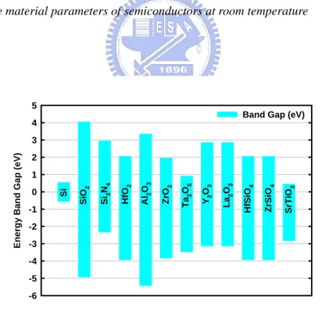
Besides, to achieve a great improvement on performance, some novel substrate materials have been also researched in recent years. In Table 1-2, it shows lots of properties of semiconductors such as germanium (Ge) and gallium Arsenide (GaAs) which own much higher carrier mobility than Silicon (Si). Because of their high cost, the epitaxy layer of Ge or GaAs on Si will be necessary for manufacture. Moreover, lots of difficult issues must be found suitable solutions. For example, Ge has an intrinsically low melt point and an unstable native oxide compared to Si [8]. Hence, how to keep the high mobility without degrading characteristics and integrate compatible processes with traditional CMOS are the purposes in the future.
All researches about CMOS encounter a revolution for new materials. Maybe Ge-channel and high-k materials with metal gate will become the main stream before long.
1-2 Motivation – Why nMOSFETs on bulk Germanium?
We have known the necessity for the development of new materials so far. One of hopeful research directions is Germanium, which provides excellent carrier mobility and a similar position of band gap to Si. Perhaps this makes Ge more adequate for integrating with conventional processes. Indeed, numbers of references has been published on this topic, and the detailed characters are shown on Table 1-2. By considering the first order approximation of drive current (Ids) at saturation operation, it is given by
) V -(V 2 1 th g 2 eff eff ox ds L W C I = μ (1.1)
,where Cox is the gate dielectric capacitance per unit area, μ is the carrier mobility, Weff and
Leff are the effective channel width and length, respectively, Vg is the applied gate voltage, and
Vth is the threshold voltage. From this equation, Ge n-type MOSFET should perform a better
operating current than p-type MOSFET ideally due to the higher mobility of electrons. However, there are many intrinsic issues of Germanium during processes, and it seems unlikely easy to solve.
The most different thing between Ge and Si is the natures of their native oxides. Unlike SiO2 with a highly thermal stability, Ge owns an unstable native oxide GeOx which is solute in H2O and can be decomposed under 300~400℃ [9]. In addition, as Table 1-2 which shows Ge has a smaller band gap than conventional Si substrate, it will results in a higher junction leakage current proportional to intrinsic carrier concentration ni (generation current) or ni2 (diffusion current). This also implies the formation of source and drain (S/D) junctions will play an important role for the performance of the devices. Actually, p-type dopants for
forming p+-n junction in Ge can be almost completely activated with a low temperature
and indicated its potential on replacement for traditional Si-based pMOSFETs; however, topics about Ge nMOSFETs are still fewer [10]. The conventional n-type dopants, such as Phosphorus (P) and Arsenic (As), have lower solid solubilities in Ge than in Si. Hence, in order to completely activate these dopants, a higher annealing temperature will be considered. Unfortunately, a relatively low melting point of Ge compared to Si makes the process window much small. Moreover, a higher activation temperature also causes significant dopant loss, junction diffusion, and degrades gate stack integrity [11-14].
On the other hand, it indicates that Ids is also related to parameter Cox from Eq. (1.1),
where Cox is determined by gate dielectric constant (ε) and its thickness (d). Because we
have mentioned that the thickness should not be thin enough to contribute a tunneling leakage current, a high-k dielectric thin film may the last choice to improve the gate capacitance. In order to achieve high quality thin film with a well controlled thickness, we exploited an ALD system to deposit Al2O3 which has a similar band gap and band offset compared with SiO2. The Eg and band alignment of some dielectric materials respective to Si are shown in Fig. 1-1. In other words, we can obtain a SiO2-like film but with a higher dielectric constant. Besides, ALD also provides a lower reaction temperature due to its mechanism – self-limiting atomic layer controlled growth [15-16] and avoids excess thermal budget as much as possible.
In brief, the related processes about Ge nMOSFETs have been known. Hence, we tried to fabricate n+-p junction diodes on bulk Germanium, and furthermore, with these results we would also investigate the Ge nMOSFETs by deposing Al2O3 and metal gate Al.
1-3 Organization of this thesis
In chapter 2, we tried to seek adequate annealing conditions for the formation of n+-p junction on bulk Ge. During the optimization, the sample activated at 500℃ for 30sec was estimated the number of remainder defects inside. Besides, by utilizing the concept which states total junction leakage currents were composed of JA and JP, we could know that the leakage current was dominated by “area” or “perimeter” component qualitatively. An quantitative extraction of JA and JP also consisted with these results, and we found no matter if a capping layer SiO2 was deposited before annealing, it exhibited defects along the perimeter of implantation region should be eliminated well, or an increasing reverse current would appear due to a large JP. However, the ratio of perimeter current to total leakage current was dependent on the dimension of our implantation area even if the defects were activated very well. In addition, we found the influence of capping layer SiO2 which was deposited just before activation was to reduce the contact resistance between Al and Ge. Hence, a higher forward current could be achieved. Subsequently, we obtained some conditions which presented very similar electrical performances of diodes, and they would be chosen to form source/drain in next chapter. Finally, an ideal value of reverse current was estimated, and it was very close to our results.
In chapter 3, we followed these results of optimization in chapter 2 to form source and drain in our Ge nMOSFETs study. By comparing with the electrical performances of Id-Vg, Id-Vd, and some electrical parameters such as source-drain resistance, dopant in-diffusion length, and sub-threshold swing, we tried to consist with our observation. However, it still showed an unacceptable series resistance.
In chapter 4, we considered the FGA process to improve the drawback in pre-chapter. It actually demonstrated both source-drain resistance and channel resistance could be much
improved. Unfortunately, the junction leakage current became out of control and much degraded the electrical performances on our Ge nMOSFETs. Some parameters were also extracted to compare together before and after FGA.
In chapter 5, it gave the conclusions for our studies and some suggestions of the thesis for the future work.
Table 1-1 ITRS 2007 Process Integration, Devices, and Structures (High-Performance Logic Technology Requirements—Near-term)
Table 1-2 Some material parameters of semiconductors at room temperature Dielectric material En er gy Ba nd Gap (eV ) -6 -5 -4 -3 -2 -1 0 1 2 3 4 5
Band Gap (eV)
Si SiO 2 Si 3 N4 Al 2 O3 HfO 2 ZrO 2 Ta 2 O5 Y2 O3 La 2 O3 Hf S iO 4 Zr SiO 4 Sr Ti O3
Chapter 2
Optimization of bulk Germanium n
+-p junction
2-1 Introduction
We have known the intrinsic performances of Ge in chapter 1. In order to accomplish nMOSFETs on bulk Ge successfully, the foremost target is to fabricate the n+-p junction with an acceptable leakage current. Conventional n-type dopants, such as Phosphorus (P) and Arsenic (As), are almost used in Si-based transistors and have high solubilities, insignificant diffusion and especially little dopant loss. However, all of these advantages are gone while Ge substrate is substituted for Si. The primary issue is that P has a relatively lower solubility, which amounts to about 1020 cm-3, in Ge than in Si [12-13]. To improve this, a higher implantation dose or a higher activation temperature will be considered. Unfortunately, a higher annealing temperature will give rise to significant diffusion and dopant loss for P in Ge. Besides, the lower melting point of Ge (939℃) than Si (ca. 1400℃) makes the thermal process window more narrow.
In this chapter, P was implanted into bulk Ge to form the n+ region, and we tried to optimize the thermal budget during activation in order to achieve perfectly electrical performances of the n+-p junction. Not only activation time and temperature, we also studied if they leaded to different electrical performances for implantation energy at 30keV and 60keV in section 2-3-3. Furthermore, we utilized the analysis of leakage paths to understand where the defects will dominate the leakage current. The detail about the method will be introduced in section 2-3-1. On the other hand, to prevent the dopant loss during activation, we deposited a capping layer SiO2 before annealing. Its effect will be shown in section 2-3-2.
Besides, we also used the analysis of secondary ion mass spectroscopy (SIMS) and four-point probe system to realize the electrical results. After above experiments, an ideal reverse leakage current will be estimated at last.
2-2 Experimental Procedures
In our diode study, p-type (Gallium (Ga), concentration ~ 2 × 10¹⁵ /cm3) Ge substrates were prepared. After broking a new wafer into adequate size, we cleaned them in diluted HF solution (HF:H2O = 1:100) and rinsed in deionized (D.I.) water alternately for several cycles. Then we treated them by a HF dip and N2 drying in order to form an H-bond passivation layer on Ge surface. Furthermore, by using a Plasma Enhanced Chemical Vapor Deposition
(PECVD) system we deposited SiO2 as the field oxide and hard mask for following
implantation. Then we defined the implantation region for n-type dopant – Phosphorous (P) – by Mask 1 and etched SiO2 by Buffer Oxide Etchant (BOE). Next, P was implanted into these samples with dose 2 × 10¹⁴ /cm2 or 1 × 10¹⁵ /cm2 at 30 or 60 keV. Subsequently, samples were activated in N2 ambient at various temperatures ranging from 500 to 700 ℃ for 30sec, 60sec, or 90sec by a rapid thermal annealing (RTA) system. Besides, the effect of capping 500
Å-thick SiO2 just before RTA process was also discussed. Then we used Mask 2 to define
contact hole and etched SiO2 till Ge surface was exposed by BOE. Without removing
photoresist (P/R) after etching, we continuously used it as lift-off mask, so the samples were directly deposited an aluminum (Al) layer as electrodes by a thermal coater system. Finally, they were proceeded the last step – lift-off – in Acetone solvent (ACE) to remove P/R and define electrodes spontaneously by Ultrasonic Sieving system. The overall fabrication processes of the n+-p junction were illustrated in Fig. 2-1 with a brief way.
To study the performances of n+-p junction, we measured the current-voltage (I-V) by HP 4156 system. Furthermore, the information of secondary ion mass spectrometry (SIMS)
and the sheet resistance (Rs) of some samples was also considered to consist with the
2-3 Results and Discussion
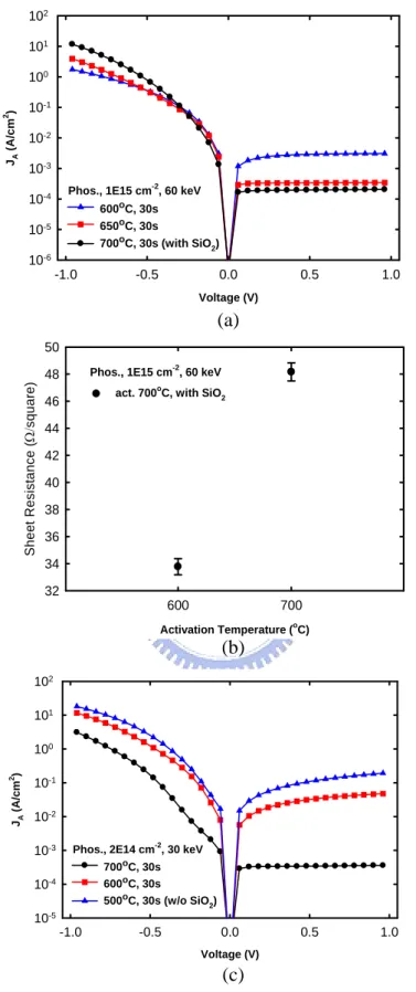
2-3-1 n
+-p junction formation on bulk Ge with different activation
temperatures
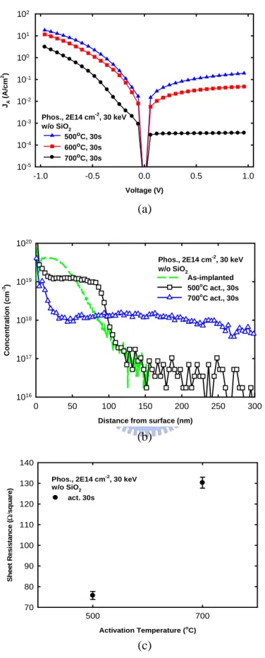
Fig. 2-2(a) indicates that the electrical characteristics of diodes are as a function of the activation temperature. We found that activation at 700℃, compared with 500℃, obviously contributed to a lower leakage current. This improvement could result from more completed dopant activation with increasing annealing temperature. Furthermore, our electrical performances, compared with some recent publications [17-18], are more excellent due to a leakage current about 10-4 A/cm2 independent on voltage bias till 1 volt can be achieved. It implies the leakage current is dominated by ideal diffusion current, and we can give a hopeful perspective on Ge nMOSFET due to the stable drain leakage current. However, the forward current is actually degraded slightly with a higher annealing temperature as well. Considering the SIMS shown in Fig. 2-2(b), it exhibits samples activated at 700℃ for 30sec accompany more significant dopant diffusion and dopant loss than those at 500℃. Therefore, a lower surface concentration for samples at 700℃ leads to a higher sheet resistance (Rs) shown in
Fig. 2-2(c). It seems that the forward current for annealing at 700℃ is degraded because of the higher Rs. But the main reason is not Rs actually. It will be further demonstrated the
degradation is related to the contact resistance (Rc) in next section. How to improve it is also
the essential topic in Ge nMOSFET fabrication, and a simple method will be introduced in next section, too.
Besides, in order to estimate the number of defects after annealing at 500℃, we considered the equation shown as below.
∫
( ) = dx x n x q Rs ) ( 1 μ , (2.1)where Rs is the sheet resistance, n(x) is the concentration of the mobile carriers from surface
(x = 0) to bulk, q is the magnitude of the electronic charge, and μ(x) is the carrier mobility. To simplify the condition, we assumedμ(x) is the same for all cases and independent on x. Finally, it becomes as below.
∫
= dx x n q Rs ) ( 1 μ (2.2)Subsequently, we also assumed all the dopants annealing at 700℃ are totally activated, so the total concentration of these carriers (
∫
n(x)dx, unit: #/cm2) would be 3.47×1020 cm-2, which was calculated by integrating the Gaussian form, which is the fitting curve of 700℃, in Fig. 2-3 (SIMS). The detail is shown as below.⎭ ⎬ ⎫ ⎩ ⎨ ⎧− − = = ) ] 2 ( [ exp ) 30 , ( 0 2 Dt x x Dt S s t x C π , (2.3)
where C is the SIMS profile, S is the limited source, D is the diffusion coefficient, t is activation time, and x0 is the position of the peak value.
20 500 0 2 18 10 3.474 ] ) 86.2 6 . 121 ( exp[ 10 354 . 1 = × ⎭ ⎬ ⎫ ⎩ ⎨ ⎧ − − × ×
∫
nm x dx nm (nm×#/cm 3 ),where the integration range is from 0 (surface) to 500 nm depth. Because the concentration is almost 1% of the peak value at 500nm, and it has less contribution on this integration. For the case of annealing at 500℃, it is almost box-shaped till 100 nm where is 1% of the peak value. Hence, the integration
∫
n(x)dx for activation at 500 ℃ becomes just n500×100 (nm×#/cm3) independent on x. Eq. (2.2) indicates Rs is inversely proportional to∫
n(x)dx. Finally, we had the relation as below.Rs500 : Rs700 = 75.74 : 130.3 = 20 10 3.474 1 : 100 1 500× × n
(green dashed line). It means the number of dopants activated at 500℃. Then, to estimate the
numbers of defects, we calculated the difference between SIMS profile and . The
calculation is shown as below.
500 n 2 13 7 18 19 10 02 . 6 ) 10 100 ( ) 10 98 . 5 10 2 . 1 ( × − × × nm× − = × cm−
Note this result is base on our assumption which states there is no defect in the case of 700℃. However, the dopants after annealing at 700℃ can’t be activated completely in real. Therefore, 6.02 × 1013 cm-2 is a “minimum” value, and it gives us the sense of the amount of defects under such process condition.
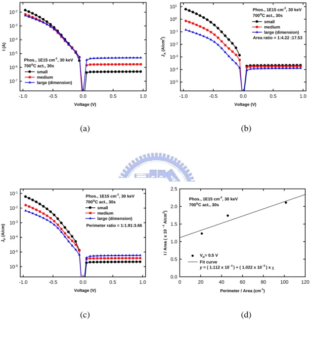
Following, we would discuss the leakage paths of reverse currents in lots of cases. Fig. 2-4 shows the box-shaped implantation region. The dashed line is the space charge edge which is a function of the voltage bias, and defects inside will contribute to a drift leakage current. It implies possible paths of leakage currents can be separated into two main parts – perimeter leakage current density (JP) and area leakage current density (JA). The former is
almost dependent on surface defects, e.g. between Ge and SiO2, in the space charge region, and the latter is dependent on bulk defects. Fig. 2-5 shows the electrical characteristics of the n+-p junction activated at 500℃ for 30sec with various implanted area. Fig. 2-5(a) displays the original data, and it implies the sheet resistance can’t be ignored due to the slightly decreasing forward current with the increasing dimension. To understand the paths of reverse leakage currents, original data in Fig. 2-5(a) is divided by ion-implanted area or ion-implanted perimeter, and the results are shown in Fig. 2-5(b) and Fig. 2-5(c), respectively. It can be understood from the total reverse leakage current shown as below.
P J A J
IR = A× + P× , (2.4)
where I R is the total leakage current, A is the implanted area, P is the perimeter of A. If I R is
divided by A or P, it will become Eq. (2.5) or Eq. (2.6), respectively.
A P J J J A I P A A R ≡ = + × (2.5)
P A P R J P A J J P I + × = ≡ (2.6)
Here we assumed JA and JP were unknown constants; the ratio of P and A were variable due
to three dimensions on our mask. If JA dominates the total leakage current, namely JP can be
ignored, Eq. (2.5) will result in the same value of J A no matter which dimension is. Or, if JP
dominates, Eq. (2.6) will show J P is a constant even through
P A
is a variable. By this analytic method, we can quickly figure out which component of leakage current (JA or JP)
dominates more in quality.
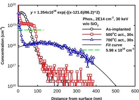
Fig. 2-5(b) indicates there are different leakage currents with various dimensions, but Fig. 2-5(c) gives the opposed result qualitatively. It means that the “perimeter” leakage current is more significant than “area” component obviously. We also used Eq. (2.5) to extract JA and JP,
and the result was shown in Fig. 2-5(d). The slope and intercept in y-axis relates to JP and JA,
respectively. Fig. 2-6 also displays samples activated at 600℃ have a similar behavior to those activated at 500℃. On the other hand, it also exhibits that JA is negative for these two
cases, but actually it should be small and positive. Maybe this linear extrapolation method doesn’t fit the real behaviors for 500℃ and 600℃ cases as it is close to the intercept of y-axis. But for the case of 700℃, it owns different characteristics in Fig. 2-7. It is obviously that the area leakage current dominates the leakage path, because Fig. 2-7(b) is more “convergent” than Fig. 2-7(c). Hence, the “area” current dominates the total leakage current. At last, the three activation conditions are also plotted together in Fig. 2-8. It reveals JP can be
reduced effectively in Fig. 2-8(b) and contributes to a lower leakage current.
Besides, we also found a smaller dimension would make perimeter current more important. a a J J a J a J I I P A P A P A ~ 4 4 2 × = × × ≡ (2.7)
Hence, as we shrink the dimension, IP will more dominate the off-state current. In other words,
2-3-2 The effect of capping SiO
2before activation
Fig. 2-9(a) shows the effect of capping SiO2 on electrical characteristics. Although the reverse currents are almost the same, the forward current is increased much for the sample capped SiO2 before activation. Furthermore, when we treated the capped sample with a longer activation time till 90sec, the forward current kept the similar behavior, but it degraded the leakage current seriously. The degradation presents that excess of thermal budget may result in precipitates of phosphorous. Therefore, those defects in Ge will give a larger leakage component [12]. Fig. 2-9(b) exhibits the SIMS profiles, and an obvious difference between the samples with and without capping layer near the surface is shown. The phenomenon seems capping SiO2 can suppress “out-diffusion” during activation due to a higher surface concentration, compared to samples without capping, even if it extends activation time till 90sec. It can be expected that a higher surface concentration should result in a lower sheet resistance. However, when we measured the sheet resistance, it indicated close values in Fig. 2-9(c). In Eq (2.1), Rs is related to the integration of the concentration profile. We attended to the SIMS profile again, and found the peak for the capped samples should have less contribution on the integration which was integrated from surface to junction depth. Accordingly, the improvement of those capped samples is not due to a smaller sheet resistance.
Another possibility of the improvement is that a lower contact resistance (Rc) may be
achieved for samples capped SiO2. Hence, we utilized the Rs data measured by the four-point
probe system to reduce a variable and considered the equation shown as below.
c s c s R R R Z d R R 2 6 . 1 2 + × = + × = (2.8)
,where R is the total resistance from the measurement of current-voltage (I-V) characteristics by the structure illustrated in Fig. 2-10(a), d and Z are shown in the figure as well, Rs is sheet
resistance, and Rc is contact resistance. The characteristics of I-V are shown in Fig. 2-10(b),
and R can be extracted at about 1volt due to the Schottky properties in small voltage bias. By Fig. 2-9(c) and Fig. 2-10(c) (circle symbols) we knew the values of Rs and R, respectively.
Hence, Rc can be estimated from Eq. (2.8), and it is plotted together with R in Fig. 2-10(c).
Because there are two contacts in our test structure, the total contact resistance is 2Rc. From
Fig. 2-10(c), 2Rc contributes a ratio more than fifty percents on total resistance obviously. In
other words, the contact resistance dominates the total resistance. More important, it also reveals a smaller Rc can be achieved for the capped samples.
Besides, Fig. 2-11(a~ b) displays the electrical characteristics of the samples capped SiO2 with various activation temperature ranging from 600℃ to 700℃. We found both the forward and reverse currents were improved with the increasing activation temperature. Comparing to these samples which are no capping layer during annealing in Fig. 2-11(c), the degradation of forward current is observed though it also improves the leakage current with increasing temperature. We contributed this difference to the effect of Rc again. To check it, the relation
between R and Rc for some samples above is presented in Fig. 2-12(a), and the details of these
conditions are shown in Table 2-1. Then, two things can be observed. First, it displays a similar result which shows 2Rc will dominate R no matter what the value of Rs is. Second,
decreasing Rc with increasing activation temperature for capped samples may be assigned to
their various surface concentrations which lead to different schottky barrier heights (ϕBn).ϕBn
will reflect on the specific contact resistances [19]. Hence, the SIMS profiles of the capped samples after annealing at 600 and 700℃ for 30sec are shown in Fig. 2-13(a). We could find these capped samples can prevent dopant loss obviously. Besides, an increasing activation temperature will result in a more severe diffusion. Combining this two effects, more dopant will accumulate near the surface with a higher activation temperature. Finally, the tendency of a decreasing contact resistance with an increasing temperature can be understood for these capped samples. Similarly, because Fig. 2-13(b) exhibits a higher activation temperature
accompanies more significant dopant loss, an opposite relation between annealing temperature and contact resistance in Fig. 2-12 can be realized as well.
As we done in pre-section, it was also extracted JA and JP from the conditions in Fig.
2-11(a). We could find the area leakage current would dominate more with increasing activation temperature from Fig. 2-14 to Fig. 2-16. The fitting lines and extracted values are compared in Fig. 2-17(a) and Fig. 2-17(b), respectively. It indicates not only more completed activation leads to smaller values of JA and JP, but also an important thing: with the increasing
annealing temperature, JP is reduced about a factor of thirty more than JA is. Hence, it proves
that JP should be eliminated well during activation to obtain good junction performances
again. A similar phenomenon was also observed in some publications [20-21]. Besides, bulk defects due to implantation have been demonstrated that they can be totally activated after annealing at temperatures ranging from 500 to 600℃ [17,22]. It consists with our extracted JA in Fig. 2-17(b) which exhibits JA is almost the same from 600 to 700℃. Namely the bulk
defects in our studies can be activated well at 600℃. Hence, a much higher annealing temperature we chosen till 700℃ is just for activating those defects along the perimeter of our implantation region. However, a directly physical proof should be checked out.
2-3-3 The effect of different implantation energies and activation times on the
electrical characteristics of diodes
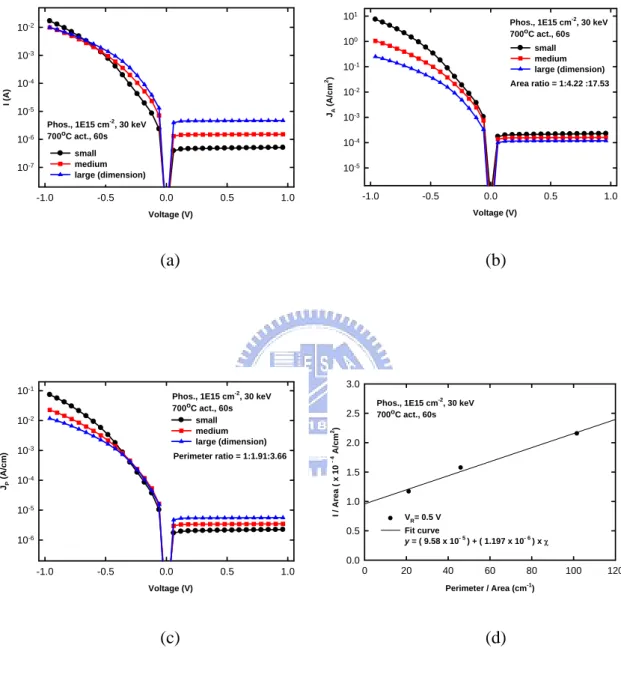
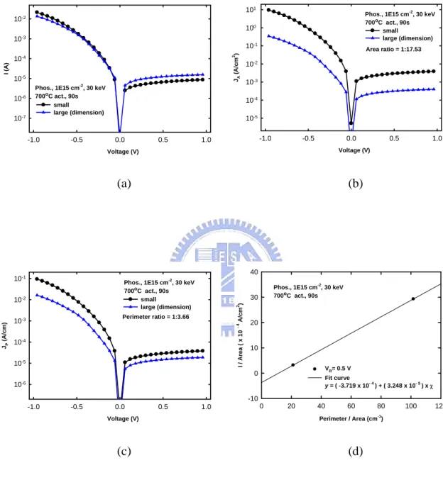
We have known some adequate process conditions, such as capping SiO2 and activation at 700℃, for the formation of n+-p junction on bulk Ge so far. In order to optimize better, some conditions of implantation energies and activation times were selected to study. In this section, all samples were capping SiO2 before annealing at 700℃, and Table 2-2 shows the conditions we proceeded. Fig. 2-18(a~b) illustrate the I-V characteristics and sheet resistance of all conditions, respectively. Activation for 30sec or 60sec results in very similar I-V
performances, but it exhibits the same degradation on leakage currents for a longer activation time till 90sec no matter which implantation energy is chosen. This degradation may result from excess of thermal budget that will result in P precipitates we mentioned before. The precipitates should be distributed from surface to a depth less than 100nm due to the SIMS profile in Fig. 2-9(b) which shows a peak at this range [12]. Then, Fig. 2-18(b) gives us the brief picture. Because the precipitates are close to the Ge surface relatively to the junction depth, which is estimated over 400nm at least, a much larger “perimeter” leakage current will be introduced due to those precipitates in the space charge region. It can consist with Fig. 2-21 and Fig. 2-24, which show JP will become larger after activation for 90sec. That may be
why the reverse current degrades after higher thermal budget.
The sheet resistance demonstrated in Fig. 2-18(c) only relates to the implantation energy, but not relates to the activation time. Furthermore, there are smaller sheet resistances for the samples at implantation energy of 60keV than 30keV, and it also responds to the forward current slightly. We attributed this to a deeper junction for implantation energy of 60keV, and it might result in a smaller Rs due to Eq. (2.1). On the other hand, it shows the study about the
paths of leakage currents from Fig. 2-19 to Fig. 2-24 again. Instead of activation for 90sec we mentioned above, it could be found the performances for activation time of 30sec and 60sec for both implantation energies were very similar. All of the four conditions exhibit “area” leakage current dominates the leak qualitatively. Of course, the condition of activation for 90sec is not suitable for our purposes of fabricating devices due to its increased leakage current. Hence, we only considered the conditions of annealing for 30sec and 60sec and plotted their figures (d) together in Fig. 2-25(a). JA and JP are extracted and illustrated in Fig.
2-25(b). Integrating the qualitative and quantitative results, it shows that these four conditions are almost undistinguishable.
At last we estimated the ideal leakage current and compared with our results. Considering the equations as below:
⎥ ⎦ ⎤ ⎢ ⎣ ⎡ − × = + = kT 1 qV s n p J J e J J (2.9) n po n p no p s L n qD L p qD J ≡ + (2.10)
, where J is the diffusion current density ideally, Jp (or Jn) are the minority hole (or electron)
current density which diffuses from p-region to n-region (or n-region to p-region), and Js is
the saturation current density. In Eq. (2.10), pno and npo are the equilibrium hole density in the
n-region and electron densities in the p-region, respectively; L and D are the minority carrier diffusion length and diffusion coefficient, and the indexes in Eq. (2.10) mean which the
region is (n or p). We also used those relation, μ L Dτ
q kT D N n n N n p a i po d i no= , = , = , = 2 2 , to substitute Eq. (2.10). Then we could calculate it as below.
) A/cm ( 10 07 . 1 ] 0259 . 0 10 87 . 1 3900 10 2 1 0259 . 0 10 6 . 8 1900 10 1 [ ) 10 4 . 2 )( 10 6 . 1 ( 1 1 2 4 5 15 7 18 2 13 19 2 − − − − × ≈ × × × + × × × × = ⎥ ⎦ ⎤ ⎢ ⎣ ⎡ × + × = q kT N q kT N qn J n n a p p d i s τ μ τ μ
From Eq. (2.9), it hints the reverse diffusion current JR should be equal: –Js. Comparing
our best performances shown in Fig. 2-17(a) to the value Js we estimated above, the ratio of
them is 2 ) ( ) ( ≈ estimated J ours J s s
. And ours diodes reach a ratio of
) ( ) ( reverse J forward J about 104.7.
2-4 Summary
We have fabricated the n+-p diodes on bulk Germanium successfully, and a reverse
current about very close to our estimated ideal value about can
be achieved. We also estimated the number of defects for samples annealing at 500℃. It gives an order of 10 2 4 A/cm 10 2× − 4 2 A/cm 10 1× − 13
cm-2. Besides, the most important thing in our studies is the analysis of paths of the leakage current. No matter if capping SiO2 before activation, we could find the total leakage current was dominated by the “perimeter” component for activation at 500 and 600℃. With an increasing temperature, it shows an interesting tendency which exhibits the area leakage current becomes more dominant than perimeter component till 700℃. Not only the qualitative analysis, we also extracted the values of JA and JP. It is demonstrated that the
elimination of perimeter defects which lead to a large value of JP is the target of activation. In
other words, we should eliminate those defects along the perimeter of implantation region effectively. Besides, the capping effect on the I-V performances of diodes is investigated in our studies. It displays a smaller contact resistance will be obtained if a SiO2 thin film is deposited before activation. In addition, samples with capping SiO2 will get a decreasing contact resistance with an increasing activation temperature from 600 to 700℃. This behavior is opposite to samples without capping layer. The phenomenon can be attributed to their different surface concentrations which lead to various energy barrier heights. We also treated implantation energies of 30keV and 60keV, but similar performances were displayed. First, activation for 90sec displays a higher leakage current whatever the implantation energy is chosen. We applied this to the formation of P precipitates which are very close to the Ge surface. Hence, a large perimeter current occurs. Second, implantation energies of 30keV and 60keV with further activation for 30sec or 60sec present identically electrical performances. And a ratio of forward to reverse current about 5 × 10⁴ at ±1 volt can be achieved.
Fig. 2-1 n+-p junction fabrication flow chart A. Wafer cleaning (HF:H2O = 1:100)
Deposit Field Oxide by PECVD
B. Define n+-region (1st mask)
Implantation (Phos.)
C. Some samples are capped SiO2. (PECVD)
D. Dopant activation (500 ~ 700℃)
E. Define contact hole (2nd mask)
Etching SiO2 by BOE
Without remove P/R
F. Al deposition (thermal coater)
(Illustration by uncapped samples)
G. Lift-off to define Al pattern in ACE
FOX Ge (p-type)
Phos.
(Capped SiO2) (Uncapped SiO2)
P/R
Voltage (V) -1.0 -0.5 0.0 0.5 1.0 JA ( A /c m 2) 10-5 10-4 10-3 10-2 10-1 100 101 102 500oC, 30s 600oC, 30s 700oC, 30s Phos., 2E14 cm-2 , 30 keV w/o SiO2 (a)
Distance from surface (nm)
0 50 100 150 200 250 300 Conc entra tion (c m -3 ) 1016 1017 1018 1019 1020 As-implanted 500o C act., 30s 700oC act., 30s Phos., 2E14 cm-2, 30 keV w/o SiO2 (b) Activation Temperature (oC) 500 700 S h ee t R es is tan ce ( Ω/ squ a re ) 70 80 90 100 110 120 130 140 act. 30s
Phos., 2E14 cm-2, 30 keV w/o SiO2
(c)
Fig. 2-2 (a) The JA-V performances of diodes activated at 500 to 700℃ for 30sec. (b) and (c)
are the measurement of SIMS and Rs, respectively. Note the samples are not capped SiO2
Distance from surface (nm) 0 100 200 300 400 500 600 Co n cen tra tio n (cm -3 ) 1016 1017 1018 1019 1020 As-implanted 500oC act., 30s 700oC act., 30s Fit curve 5.98 x 1018 cm-3
Phos., 2E14 cm-2, 30 keV
w/o SiO2
y = 1.354x10¹⁸ exp(-((x-121.6)/86.2)^2)
Fig. 2-3 It shows the fitting line of activation at 700℃ (solid curve) and an estimated
activation level after annealing at 500℃ (green dashed line). Note the samples are not
capped SiO2 before annealing.
a
a
Fig. 2-4 This picture illustrates the paths of junction leakage currents. The box-shaped is the implantation region of Phosphorus with a perimeter of a. The dashed line is the edge of space charge region, and defects inside will contribute to a drift leakage current. We separated the
current into two main parts, J and J .
P
P
J
AJ
PVoltage (V) -1.0 -0.5 0.0 0.5 1.0 I ( A ) 10-5 10-4 10-3 10-2 10-1 small medium large (dimension) Phos., 2E14 cm-2 , 30 keV 500oC act., 30s, no SiO 2 cap Voltage (V) -1.0 -0.5 0.0 0.5 1.0 JA (A/ c m 2) (a) (b) (c) (d)
Fig. 2-5 (a) The I-V characteristics of junctions activated at 500℃ for 30sec with various
dimensions. (b) and (c) show the JA-V and JP-V characteristics, respectively. It hints the
“perimeter current” dominates the leakage current qualitatively. (d) It shows the extracted JA
and J quantitatively. Note the samples are not capped SiO before annealing.
10-3 10-2 10-1 100 101 102 small medium large (dimension) Phos., 2E14 cm-2 , 30 keV
500oC act., 30s, no SiO2 cap
Area ratio = 1:4.22 :17.53 Perimeter / Area (cm-1 ) 0 20 40 60 80 100 12 Voltage (V) -1.0 -0.5 0.0 0.5 1.0 JP (A /cm ) 10-5 10-4 10-3 10-2 10-1 100 small medium large (dimension) Phos., 2E14 cm-2 , 30 keV 500oC act., 30s, no SiO 2 cap Perimeter ratio = 1:1.91:3.66 0 I / Area ( x 10 - 2 A/cm 2) -2 0 2 4 6 8 10 12 14 VR = 0.5V Fit Curve y = (-6.172 x 10⁻³ ) + (1.146 x 10⁻³ ) χ Phos., 2E14 cm-2 , 30 keV 500oC act., 30s, no SiO 2 cap