行政院國家科學委員會專題研究計畫 成果報告
具有形變通道之互補式金氧半元件製作與分析
計畫類別: 個別型計畫 計畫編號: NSC93-2215-E-009-033- 執行期間: 93 年 08 月 01 日至 94 年 07 月 31 日 執行單位: 國立交通大學電子工程學系暨電子研究所 計畫主持人: 黃調元 計畫參與人員: 林宏年、盧景森、徐行徽、藍文廷、李聰杰 報告類型: 精簡報告 報告附件: 出席國際會議研究心得報告及發表論文 處理方式: 本計畫可公開查詢中 華 民 國 94 年 11 月 7 日
行政院國家科學委員會補助專題研究計畫
■ 成 果 報 告
□期中進度報告
具有形變通道之互補式金氧半元件製作與分析
Fabrication and characterization of CMOS devices with strained channel
計畫類別:■ 個別型計畫 □ 整合型計畫
計畫編號:NSC 93-2215-E-009-033
執行期間:93 年 08 月 01 日 至 94 年 07 月 31 日
計畫主持人:黃調元 教授
計畫參與人員:
林宏年、盧景森、
徐行徽
、
藍文廷
、
李聰杰
成果報告類型(依經費核定清單規定繳交):■精簡報告 □完整報告
本成果報告包括以下應繳交之附件:
□赴國外出差或研習心得報告一份
□赴大陸地區出差或研習心得報告一份
□出席國際學術會議心得報告及發表之論文各一份
□國際合作研究計畫國外研究報告書一份
處理方式:除產學合作研究計畫、提升產業技術及人才培育研究計畫、
列管計畫及下列情形者外,得立即公開查詢
□涉及專利或其他智慧財產權,□一年□二年後可公開查詢
執行單位:國立交通大學電子工程研究所
中 華 民 國 年 月 日
2
具有形變通道之互補式金氧半元件製作與分析
“Fabrication and characterization of CMOS devices with strained channel”
計畫編號:NSC93-2215-E-009-033 執行期間:93 年 8 月 01 日 至 94 年 7 月 31 日 主持人:黃調元 交通大學電子工程系教授 中文摘要 在本報告中,我們主要探討單軸形變通道 之奈米級互補式金氧半元件之通道背向散射 特性分析。通道背向散射比在單軸伸張應力下 或單軸壓縮應力下分別將增加或減少。我們發 現,在次100 奈米級元件中,背向散射載子平 均自由路徑之形變造成的調變及 kBT 層厚度 的減少是造成具有不同背向散射比的原因。此 外,不管形變極性如何,源極端注入速度將改 善。我們也將藉由彈道效率及注入速度分析通 道背向散射比對於驅動電流的影響。 關鍵字:金氧半元件、散射、單軸形變。 Abstracts
In this work, we have investigated the channel backscattering characteristics of uniaxially strained nanoscale CMOSFETs. Channel backscattering ratio increases and decreases under uniaxial tensile and compressive strain, respectively. It is found that in sub-100 nm devices, strain-induced modulation of carrier mean-free-path for backscattering and reduction in kBT layer thickness are responsible for the different behaviors of backscattering ratio. Nevertheless, the source-side injection velocity improves irrespective of the strain polarities. The impact of channel backscattering ratio on drive
current is also analyzed in terms of ballistic efficiency and injection velocity.
Keywords: MOSFETs 、 scattering 、 uniaxial
strain.
Introduction
Recently various strain techniques are actively pursued to give the device performance a much needed boost in 90 nm node and beyond [1]–[3]. Mobility enhancement induced by strain in the channel has been widely characterized, however, only half of the mobility enhancement is all that needed to account for the observed saturation drain current increase [4]. To reconcile with this discrepancy and to understand ballistic transportation in nanoscale transistor, carrier backscattering theory has been proposed. As illustrated in the inset of Fig. 1, some of the injected carriers are backscattered near the source end of channel region within a
kBT layer which has a potential drop of kBT / q and thickness of l0. Since the transmitted carriers ultimately determine the drive current, carrier backscattering ratio r and injection velocity υinj at the top of source-channel barrier are both critical in determining the drive current Idsat. For higher Idsat, reducing r and increasing υinj are desirable [5]. It has been reported that biaxial tensile strain results in backscattering ratio reduction with Si0.7Ge0.3 virtual substrate from
simulation [6]. However, the influence of uniaxial strain on backscattering ratio has not been clarified yet. In this paper, we report the impact of uniaxial process-induced tensile and compressive strains on channel backscattering ratio for the first time. In addition, the impact of channel backscattering ratio on drive current is also analyzed in terms of mean-free-path (MFP),
kBT layer thickness, ballistic efficiency, and injection velocity.
Experimental
Process-strained Si (PSS) MOSFETs fabricated by state-of-the-art CMOS process are studied in this work [2]. Schematic structure with uniaxial strain engineering is illustrated in Fig. 1, where uniaxial tensile strain for nMOSFETs and uniaxial compressive strain for pMOSFETs are achieved. To minimize barrier height modulation from drain-induced barrier lowering (DIBL), PSS and control devices with nominally identical DIBL and subthreshold swing are characterized (inset of Fig. 2). Drive current improvement of both PSS devices relative to control devices is shown in Fig. 2, all devices with identical inversion C-V characteristics. From scattering theory in [6], drive current in saturation region (|Vd|= 1 V) can be expressed as
(
g Tsat)
sat sat inj dsat C V V r r υ W I OX , 1 1 − ⎥ ⎦ ⎤ ⎢ ⎣ ⎡ + − = (1)where υinj, rsat, and VT,sat represent injection velocity, backscattering ratio, and threshold voltage, respectively. The ratio rsat is a function of carrier mean-free-path for backscattering λ0 and kBT layer thickness l0 ( rsat= 1 / [ 1 + λ0 / l0 ] ) [8]. The VT,sat is determined by maximum
transconductance (Gm,max) method with DIBL consideration ( ∆VDIBL= VT,lin@|Vd|=10 mV –
VT,sat@|Vd|=1 V, where VT is defined as the gate voltage when |Id|= 0.1W/L µA ), i.e., VT,sat=
VT,lin(Gm,max@|Vd|=10 mV) – ∆VDIBL. Then, a temperature-dependent analytical model is employed to extract the λ0 / l0 ratio using the following analytic expression
sat T g V V η l λ T α , 0 0 2 4 2 1 1 − − ⎥ ⎦ ⎤ ⎢ ⎣ ⎡ + − = (2) where α and η represent temperature sensitivity of Idsat and VT,sat, i.e., α= ( Idsat1 – Idsat2 ) / ( T1 – T2 ) and η= ( VT,sat1 – VT,sat2 ) / ( T1 – T2 ) [8]. The measurement temperature is decreased from 298 K to 228 K at a step of 15 K. α and η are extracted from the best-fitted slopes of ∆Idsat and ∆VT,sat at different temperatures. The λ0 / l0 ratio can then be calculated by (2). Lastly, backscattering ratio and ballistic efficiency B (= [ 1 – rsat ] / [ 1 + rsat ] ) can be deduced.
Results and Discussion
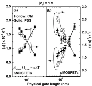
The gate length dependence of backscattering factors, |α|, λ0 / l0, rsat, and B are shown in Figs. 3 and 4. In Fig. 3, |α| is the dominant factor in determining λ0 / l0 of MOSFETs since the ratio η / (Vg – VT,sat) (|η|= 0.5 to 0.9 mV/K) is ten times smaller than |α|. Compared with control devices, PSS nMOSFET demonstrates slight increase in λ0 / l0, while PSS pMOSFET shows significant decrease. Comparing to rsat of control devices, the tensile-strained PSS nMOSFET has smaller rsat whereas compressive-strained PSS pMOSFET has larger rsat. This phenomenon indicates that injected electrons in tensile-strained nMOSFET exhibit less channel backscattering while
4
injected holes in compressive-strained pMOSFET suffer more backscattering. The rsat difference between control and PSS devices becomes more dramatic as Lphysical is shorter than 0.1 µm. It is also shown that the ballistic efficiency of tensile-strained PSS nMOSFET is improved but that of compressive-strained PSS pMOSFET is degraded. Qinv for characterized devices is extracted from MOSFETs with an area of 100 µm2 under strong inversion, taking into account VT roll-off and DIBL [9]. υinj can then be calculated by Idsat= WυinjBQinv. As shown in Fig. 5, the injection velocity is improved in both PSS devices, which is ascribed to process-strained induced reduction in carrier effective mass [1]. As shown in the inset of Fig. 5, ∆Idsat can be related to the sum of ∆υinj and ∆B. Slight underestimation of ∆Idsat in NMOS is due to minor Qinv difference between PSS and control devices. To further investigate the mechanism of strain-induced backscattering modulation, λ0 is deduced from the expression λ0= ( 2 kBT / q ) µ0 /
υinj [4], where the low field mobility µ0 is extracted by the resistance slope-based method [10]. From the ratio of λ0 / l0, l0 can be calculated. It is found thatl0 of both PSS devices is reduced to about 90% of that of control devices, and the thinning of l0 may be due to the strain-induced bandgap shift causing sharper potential profile. In addition, λ0 is increased in PSS nMOSFETs, which is consistent with the simulation results of [11]. Contrary to nMOSFETs, PSS pMOSFETs exhibit smaller λ0 than that of control devices, which is probably due to the compressed lattice in the channel inducing much severe carrier scattering. Hence, it is essential to improve not only injection velocity but also ballistic efficiency in order to further enhance the
performance of uniaxial-strained MOSFETs in nanoscale regime. Although Idsat of PSS pMOSFETs is improved through the enhancement of injection velocity at the expense of ballistic efficiency loss, ultimate PSS performance boost should therefore be expected if one could conceive a clever method to enhance ballistic efficiency without sacrificing injection velocity.
Conclusions
In this letter, the influence of uniaxial strain on channel backscattering ratio in nanoscale MOSFETs is investigated. Channel backscattering ratio is reduced in tensile-strained
nMOSFET but increased in
compressive-strained pMOSFET, notwithstanding the increased carrier injection
velocity in both cases. Drive current is determined not only by backscattering ratio but also injection velocity. Strain techniques or device structures with simultaneous improvement of channel backscattering ratio and injection velocity are therefore favorable for ultimate performance boost in mesoscopic regime.
References
[1] S. E. Thompson, enyon, J. Klaus, K. Kuhn, Z. Ma, B. Mcintyre, K. Mistry, A. Murthy, B. Obradovic, R. Nagisetty, P. Nguyen, S. Sivakumar, R. Shaheed, L. Shifren, B. Tufts, S. Tyagi, M. Bohr, and Y. El-Mansy, “A 90-nm logic technology featuring strained-silicon,” IEEE
Trans. Electron Devices, vol. 51, pp. 1790–1797, Nov.
2004.
[2] C.-H. Ge, C.-C. Lin, C.-H. Ko, C.-C. Huang, Y.-C. Huang, B.-W. Chan, B.-C. Perng, C.-C. Sheu, P.-Y. Tasi, L.-G. Yao, C.-L. Wu, T.-L. Lee, C.-J. Chen, C.-T. Wang, S.-C. Lin, Y.-C. Yeo, and C. Hu, “Process-strained Si (PSS) CMOS technology featuring 3D strain engineering,” in IEDM Tech. Dig., 2003, pp. 73–76.
[3] T. Ghani, M. Armstrong, C. Auth, M. Bost, P. Charvat, G. Glass, T. Hoffmann, K. Johnson, C. Kenyon, J. Klaus, B. Mclntyre, K. Mistry, A. Murthy, J. Sandford, M. Silberstein, S. Sivakumar, P. Smith, K. Zawadzki, S. Thompson, and M. Bohr, “A 90nm high volume manufacturing logic technology featuring novel 45nm gate length strained silicon CMOS transistors,” in IEDM Tech.
Dig., 2003, pp. 978–980.
[4] M. Lundstrom, “On the mobility versus drain current relation for a nanoscale MOSFET,” IEEE Electron Device
Lett., vol. 22, pp. 293–295, June 2001.
[5] M. Lundstrom, “Elementary scattering theory of the Si MOSFET,” IEEE Electron Device Lett., vol. 18, pp. 361–363, July 1997.
[6] T. Skotnicki, “Transistor scaling to the end of the roadmap,” in Short Course of Symp. VLSI Tech., Honolulu, Hawaii, Jun. 2004.
[7] A. Rahman, and M. S. Lundstrom, “A compact scattering model for the nanoscale double-gate MOSFET,”
IEEE Trans. Electron Devices, vol. 49, pp. 481–489, Mar.
2002.
[8] M.-J. Chen, H.-T. Huang, K.-C. Huang, P.-N. Chen, C.-S. Chang, and C. H. Diaz, “Temperature dependent channel backscattering coefficients in nanoscale MOSFETs,” in IEDM Tech. Dig., 2002, pp. 39–42.
[9] A. Lochtefeld, and D. A. Antoniadis, “On experimental determination of carrier velocity in deeply scaled NMOS: how close to the thermal limit?” IEEE
Electron Device Lett., vol. 22, pp. 95–97, Feb. 2001.
[10] K. Rim, S. Narasimha, M. Longstreet, A. Mocuta, and J. Cai, “Low field mobility characteristics of sub-100 nm unstrained and strained Si MOSFETs,” in IEDM Tech. Dig., 2002, pp. 43–46.
[11] C. Jungemann, and B. Meinerzhagen, “MC simulation of strained Si/SiGe devices,” in Proc.
ESSDERC, 2003, pp. 9–14. 此計畫之論文發表 1. SSDM, 2004, p.716-717. 2. SISC, 2004, p.781-784. 3. VLSI Tech., 2005, p.174. 4. EDL-26, 2005, p.676. 5. SSDM, 2005, p.874-875.
6
Fig.1. Schematic structure of process-strained Si (PSS) MOSFETs. Various stress -engineered processes are employed to achieve uniaxially tensile and compressive strains for nMOSFETs and pMOSFETs, respectively. The inset illustrates that carrier in kBT layer region is with a backscattering ratio r where the thickness of
kBT layer is l0.
Fig.2. Id-Vd characteristics of control and PSS MOSFETs. With identical subthreshold swing and DIBL to those of control devices (as shown in the inset), both PSS nMOSFET and pMOSFET exhibit about 19% and 36% improvement of drive current at |Vg – VT,sat|= |Vd|= 1 V.
Fig.3 Comparison of temperature sensitivity of drive current |α|, and ratio of mean-free-path (MFP) for backscattering over kBT layer thickness λ0 / l0 between control devices, and PSS (a) nMOSFETs, (b) pMOSFETs.
Fig. 4 Effects of uniaxial (a) tensile-strained nMOSFETs, and (b) compressive-strained pMOSFETs on channel backscattering ratio rsat and ballistic efficiency B.
Fig. 5 ∆υinj and ∆B as a function of ∆Idsat for PSS nMOSFETs (square symbol) and pMOSFETs (triangle symbol). The solid line indicates that ∆υinj (or ∆B) varies linearly with ∆Idsat. For PSS nMOSFETs, both carrier injection velocity and ballistic efficiency are higher than control devices. While for PSS pMOSFETs, slightly lower B and much higher υinj are obtained. The inset shows the variation percentage of parameters of PSS devices (nMOSFETs,
Lphysical= 55 nm, pMOSFETs, Lphysical= 75 nm) relative to those of control devices. ∆Idsat can be related to the sum of ∆υinj and ∆B.