國
立
交
通
大
學
電子工程學系 電子研究所碩士班
碩
士
論
文
適用於 H.264 解碼器的可調式雙層外部記憶體管理器
A Flexible Two-Layer External Memory Management for
H.264/AVC Decoder
研 究 生:張長軒
指導教授:黃 威 教授
適用於 H.264 解碼器的可調式雙層外部記憶體管理器
A Flexible Two-Layer External Memory Management for H.264/AVC Decoder研 究 生:張長軒 Student:Chang-Hsuan Chang
指導教授:黃 威 教授 Advisor:Prof. Wei Hwang
國 立 交 通 大 學
電 子 工 程 學 系 電 子 研 究 所
碩 士 論 文
A Thesis
Submitted to Department of Electronics Engineering & Institute of Electronics College of Electrical Engineering and Computer Engineering
National Chiao Tung University in partial Fulfillment of the Requirements
for the Degree of Master
in
Electronics Engineering
June 2006
Hsinchu, Taiwan, Republic of China
適用於
H.264 解碼器的可調式雙層記憶體管理器
學生:張長軒 指導教授:黃 威 教授
國立交通大學電子工程學系電子研究所
摘 要
在 H.264 解碼器中有大量的資料需要去存取記憶體,外部記憶體資料存取所 需的時間和功率消耗對於整個 H.264 系統的效能影響很大,因為外部記憶體受到 頻寬的限制所以外部記憶體的效能對於系統仍然是個瓶頸.在 H.264 解碼器中為 了達到即時播放的效果,如何設計一個良好的記憶體子系統變的十分重要. 在這篇論文中,我門針對 H.264 解碼器提出了一個計憶體子系統,這個子系統 包含了一個可調變的記憶體控制器,靜態隨機存取記憶體,雙倍數同步動態隨機存 取記憶體,和一條匯流排. 子系統裡面的記憶體控制器除了要確保資料傳輸的正確性以外還要能改善 外部記憶體的效能,我們所提出來的記憶體控制器共分成兩層,第一層是用來做位 址轉換,這一層提供了一個存取記憶體的位址產生方法,這個方法可以就由減少記 憶體中誤失的數目來達到節省功率的效果. 第二層是外部記憶體介面,除了產生適當的命令給記憶體外還可以降低因為 記憶體誤失所耗費的時間,這個記憶體介面可以用來控制單倍數和雙倍數同步動 態隨機存取記憶體,因為這個外部記憶體介面的可調變性,使用者可以快速的把這 個介面隨著不同型態的外部記憶體整合到系統裡. 這個 H.264 解碼器中的記憶體控制器可以減少資料存取延遲時間到大約 30%,而且頻寬的使用率可以從 42%提升到 51%左右.A Two-Layer Flexible External Memory Management for
H.264/AVC Decoder
Student : Chang-Hsuan Chang
Advisors : Prof. Wei Hwang
Department of Electronics Engineering & Institute of Electronics
National Chiao-Tung University
ABSTRACT
In the H.264/AVC decoder there are large amount of data need to be fetched to/from the off-chip memory. The latency of accessing data and power consumption in the off-chip memory greatly affect the performance of the whole system. The performance of the off-chip memory is still the bottleneck of the video process due to the limited bandwidth. The real-time requirement in H.264/AVC decoder at level 4 result in the request of a well designed memory sub-system.
In this thesis, we proposed a memory sub-system for the H.264/AVC decoder. This memory sub-system contains a flexible memory controller, SRAM, AHB-bus, and DDR SDRAM.
This memory controller inside the memory sub-system not only keeps the correctness of the data transfer between the module and DRAM but is also responsible to improve the performance of the external memory. The proposed memory controller consists of two layers. The first layer is address translation which provide an efficient memory map method. This layer is designed to decrease the number of row-miss status and bank-miss status. By this way the power consumption can be saved.
The second layer is external memory interface. Besides generate appropriate commands to the off-chip memory, this layer is used to increase bandwidth utilization and decrease the latency induced by the row-miss status and bank-miss status. This external memory interface is design to control the SDR SDRM and DDR SDRAM. Due to the flexibility of this EMI, the users can rapidly integrate this EMI into their system design with various kind of external memory.
The experimental results of a H.264 decoder show that the proposed controller can further reduce access latency by approximately 30% and the memory utilization is
Acknowledgements
我要感謝我的老師黃威教授這兩年對我的指導和鼓勵,在研究過程中提供了 很多方向和指引,才讓我的研究可以順利完成,特別感謝老師能讓我同時結合記憶 體和多媒體這個研究領域,讓我這兩年的研究雖然辛苦但是充滿了樂趣. 另外要特別的感謝就是跟我同一個團隊的老師,學長和同學,要謝謝蔣迪豪教 授讓我加入他們研究的 H.264 (TLM)團隊.使我有機會可以接觸多媒體這一塊領 域.在團隊工作期間,成功大學的李國君教授給了我門團隊很多的指導,我們的團 隊的主導人彭文孝學長,日前已經到資工系當教授了,更是提供了很多不同的方向 讓我們來思考,從學長的身上學到很多東西. 另外要特別由衷感謝給我最多幫助的同一個團隊的博班學長李志鴻和陳治 傑同學,在研究過程給了我相當多的支援與協助,才使得我的論文可以順利完成 接下來要感謝同一個實驗室的黃柏蒼學長,華重憲學長,和張銘宏學長,在我的研 究過程幫助了我很多也教導了我很多,從學長身上得到很多寶貴的建議. 最後要感謝我的家人和朋友在研究過程給我的打氣與鼓勵以及關心,讓我的 研究過程雖然辛苦但還是充滿歡樂.Contents
Chapter 1 Introduction...1
1.1 Background ...1
1.2 Motivation...2
1.3 Organization...3
Chapter 2 Overview of External Memory Organization ...5
2.1 DRAM characteristic ...5
2.1.1 DRAM architecture...5
2.1.2 DRAM command and operation ...6
2.2 Past DRAM controller techniques ...8
2.2.1 Techniques and Improvement ...9
2.3 Modern DRAM Development ...15
2.3.1 Bandwidth ...15
2.3.2 Latency...17
2.3.3 Power ...19
2.4 Future trend of DRAM...22
Chapter 3 Transaction Level Modeling of H.264/AVC Decoder ...25
3.1 Overview of H.264...25
3.1.1 Introduction...25
3.1.2 Characteristic of H.264 ...27
3.2 Transaction Level Modeling ...29
3.2.1 Introduction of TLM ...29
3.2.2 Design flow with TLM ...31
3.3 Transaction Level Modeling of H.264 Decoder ...34
3.3.1 Specification ...34
3.3.2 System Architecture of H.264 decoder ...36
3.3.2.1 Video Pipe...37
3.3.2.2 System Schedule ...39
3.3.2.3 System Modeling ...41
3.4 Memory Controller in H.264 Decoder...42
Chapter 4 External Memory Interface ...45
4.1 Concept of EMI...46
4.2 Architecture of EMI ...47
4.2.1 FIFO...48
4.2.2 Mode Control ...52
4.2.3 Finite States Machine and schedule block ...54
4.2.3.2 Schedule block ...56
4.2.4 Counter and Timing Checker ...57
4.3 The external memory in H.264 decoder...59
4.4 Analysis...61
4.4.1 Access Latency...61
4.4.2 Power Estimation ...61
4.4.3 Auto-pre-charge Method Effect ...63
4.4.4 FIFO Size Effect ...66
4.5 Summary ...69
Chapter 5 Address Translation Machine & Memory Subsystem for
H.264 Decoder ...71
5.1 Introduction...71
5.2 Memory Subsystem Architecture...74
5.3 Data Arrangement ...76
5.3.1 Memory Mapping Method...76
5.3.2 Latency Estimation ...80
5.3.3 Data Bus Schdule...84
5.4 Address Translation...86
5.5 Analysis & Simulation Result...87
5.5.1 Design for worst case...87
5.5.2 Design for average case ...96
5.6 Summary ...99
Chapter 6 Conclusions and Future work ...101
6.1 Conclusions...101
6.2 Future Work ...102
List of Figures
Fig. 2.1 Simplified architecture of a DRAM. ...5
Fig. 2.2 Bank state diagram. ...7
Fig. 2.3 Read command CAS latency. ...8
Fig. 2.4 Write command (SDRAM)...8
Fig. 2.5 Write command (DDR). ...8
Fig. 2.6 Data placement ...10
Fig. 2.7 Mode control prediction ... 11
Fig. 2.8 Mode control memory controller... 11
Fig. 2.9 2-stage scheduler memory controller ...12
Fig. 2.10 recompression method ...13
Fig. 2.11 Operating frequency of SDR, DDR-1, DDR-2...15
Fig. 2.12 Timing diagram of DDR & DDR-2...16
Fig. 2.13 CPU VS DRAM performance ...17
Fig. 2.14 Accesses addressed to same bank...18
Fig. 2.15 Accesses addressed to different bank ...18
Fig. 2.16 Clock stop mode ...21
Fig. 2.17 The required data rate in 3DG engine...24
Fig. 3.1 Scope of video coding standardization...26
Fig. 3.2 System model at different levels of abstraction...30
Fig. 3.3 Design floe with transaction level modeling ...32
Fig. 3.4 System architecture diagram ...36
Fig. 3.5 De-blocking process order...38
Fig. 3.6 Transaction level modeling at system level...41
Fig. 3.7 Relationship between H.264 decider and external memory ...42
Fig. 3.8 Architecture of the memory controller in H.264 decoder...43
Fig. 4.1 Architecture of my memory controller ...45
Fig. 4.2 Connection of EMI ...46
Fig. 4.3 Architecture of EMI...47
Fig. 4.4 Consecutive accesses to same row (burst length=4) ...48
Fig. 4.5 Consecutive accesses to different row (burst length=4) ...49
Fig. 4.6 Consecutive accesses to different row with auto-pre-charge ...49
Fig. 4.7 Command FIFO...50
Fig. 4.8 State diagram of bank-miss status ...52
Fig. 4.9 State diagram of row-hit and row-miss status ...53
Fig. 4.10 Mode control block...53
Fig. 4.12 Finite State Machine ...55
Fig. 4.13 Command with schedule and without schedule (two bank-miss) ...56
Fig. 4.14 Command with schedule and without schedule (two row-miss) ...57
Fig. 4.15 Read operation of SDR and DDR...60
Fig. 4.16 Write operation of SDR and DDR ...60
Fig. 4.17 Latency of different method for video process...64
Fig. 4.18 Latency of different method for random process ...65
Fig. 4.19 Latency of different method for video process_1...65
Fig. 4.20 Dynamic method 1 versus row-open method in the video process ...66
Fig. 4.21 Architecture of stall machine...67
Fig. 4.22 Respond latency v.s read-data-FIFO Size...67
Fig. 4.23 Respond latency v.s write-data-FIFO Size ...68
Fig. 5.1 The memory controller in H.264 decoder ...73
Fig. 5.2 Memory subsystem Architecture ...74
Fig. 5.3 Architecture of memory organization...76
Fig. 5.4 Frame map to memory...77
Fig. 5.5 Memory map to frame ...78
Fig. 5.6 Frame map to memory (1 or 2)...79
Fig. 5.7 Worst case of accessing a 4 x 4 luma block (P frame)...81
Fig. 5.8 Worst case of accessing a 8 x 8 luma block (B frame) ...82
Fig. 5.9 Read operation for motion compensation...82
Fig. 5.10 Read operation for motion compensation...85
Fig. 5.11 Layer 1 architecture ...86
Fig. 5.12 Read operation for motion compensation...87
Fig. 5.13 Display order & Decode order...89
Fig. 5.14 Latency of different frame ...93
Fig. 5.15 Active number of different frame ...94
Fig. 5.16 Pre-charge number of different frame ...94
Fig. 5.17 Bus utilization of different frame ...95
Fig. 5.18 The efficiency of DRAM access for MC...97
Fig. 5.19 The efficiency of DRAM access for MC,DB, and DEI...97
Fig. 5.20 Average cycle count of DRAM access per MB ...98
Fig. 5.21 The distribution of DRAM commands per MB...98
List of Tables
Table 2.1 Related works of SDRAM memory controller ...14
Table 2.2 Current of different condition ...20
Table 2.3 Amount of memory will be refreshed ...20
Table 3.1 Characteristics of different models ...31
Table 3.2 Level limits ...35
Table 3.3 System schdule...40
Table 4.1 Different method for receiving a picture...51
Table 4.2 Timing parameters of Micron Mobile DDR DRAM ...58
Table 4.3 Status of different process ...61
Table 4.4 Power of each state ...62
Table 4.5 State transition of different process...63
Table 5.1 Dram requirement for real time requirement in design of worst case...75
Table 5.2 Different memory mapping method for different memory configuration77 Table 5.3 Cycle count of each module in worst case ...83
Table 5.4 EMI setting...88
Table 5.5 Key parameters of micron Mobile-DDR SDRAM ...89
Table 5.6 Number of commands in each frame (Luma) ...90
Table 5.7 Some cases in the memory (Luma)...91
Table 5.8 Some cases in the memory (Luma)...92
Chapter 1
Introduction
1.1 Background
Multimedia processing technologies have been widely applied in many systems.
These technologies have not only provided existing applications like desktop
video/audio but also spawned brand new industries and services like digital video
recording, video-on-demand services, high-definition TV, etc. To support complex
multimedia applications, architectures of multimedia systems must provide high
computing power and high data bandwidth. Furthermore, a multimedia operation
system should support real-time scheduling.
Previous researches have shown that data transfer and storage of
multidimensional array signals dominate the performance and power consumption in
system-on-a-chip (SoC) designs. In particular, the data transfer to off-chip memory is
especially important due to the scarce resource of off-chip bandwidth. In fact,
although the tremendous progress in VLSI technology provides an ever-increasing
number of transistors and routing resource on a single chip, and hence allows
integrating heterogeneous control and computing functions to realize SoCs, the
improvement on off-chip communication is limited due to the number of available
input/output (I/O) pins and the physical design issues of these pins. As many recent
studies have shown, the off-chip memory system is one of the primary performance
1.2 Motivation
As the resolution of video-processing applications becomes high, video signal
processors should deal with a large amount of data within a tightly bounded time. Due
to the large quantities, video data are stored in off-chip memories that are usually slow,
and thus the system performance strongly depends on the memory bandwidth between
processors and external memories. For example, in decoding MP@HL video streams,
an MPEG-2 video decoder must feature 10-MB memory as frame buffers and should
access about 370 million data/s.
H.264/AVC is the newest international video coding standard. Relative to prior
video coding methods such as MPEG-2 video, H.264/AVC has the higher coding
efficiency. With an increasing number of services and growing popularity of high
definition TV are creating greater request for higher coding efficiency. Moreover,
other transmission media such as Cable Modem, XDSL, or UMTS offer much lower
data rates than broadcast channels, and enhanced coding efficiency can enable the
transmission of more video channels or higher quality video representations within
existing digital transmission capacities.
In the H.264 decoder, it process 245760 MB/s in maximum at level 4. In order to
support the complex mode in the H.264 decoder, there are even large data transfer
between H.264 decoder and external memory.
The issue of latency, bandwidth utilization, and power consumption are very
important in the video process. These issues in the video process are greatly
influenced by the memory subsystem. Hence a memory controller that can efficiently
communicate with external memory is the most significant part over the entire video
dominates the total amount of data transmission especially when SDRAM is adopted
as external frame memories. How to manage the data transfer and utilize the limited
bandwidth is the most important issue of the memory controller.
1.3 Organization
The organization of this thesis is as follows. An overview of external memory
organization is introduced in Chapter 2. Besides the DRAM architecture and basic
operation the past DRAM controller will be described. The DRAM development and
DRAM trend are also discussed here.
My memory controller is applied in the H.264 decoder. This H.264 decoder is
designed in transaction level model (TLM). The concept of TLM and the TLM model
of our H.264 decoder will be thoroughly explained in Chapter 3. The role of my
controller in this H.264 is mentioned here. There are two layers in my memory
controller. Layer 0 is used to control the memory. Layer 1 is used to improve the
performance in video process.
Chapter 4 presents layer 0 of my memory controller. This layer is called external
memory interface (EMI). The system can communicate with external memory by
using this EMI. The flexibility if this EMI can help users to integrate this EMI to their
design easily. The different setting of EMI will influence the performance. The
improvement on performance including latency and power will be compared here.
The experimental results of different setting will also be listed in this chapter.
The whole memory subsystem and the layer 1 of my memory controller which is
needs large amount of data transfer. The efficiency of the memory controller is very
important. To deal with the bandwidth loss which degrades the performance, the layer
1 is combined into my memory controller. We have proposed a memory map method
by using the characteristic of the H.264 process, and Layer 1 is used to do the address
translation. This address translation machine not only reduces the power consumption
on the bus line but also increases the bandwidth utilization. Finally, the conclusions
Chapter 2
Overview of External Memory
Organization
In this chapter, it introduces the overview of external memory organization for video process. Firstly, DRAM characteristic is described in section 2.1. Then, section 2.2 discussed the techniques which were proposed in the past used in memory controller. In addition, the design trends of modern DRAM is presented in section 2.3.
2.1 DRAM characteristic
2.1.1 DRAM architecture
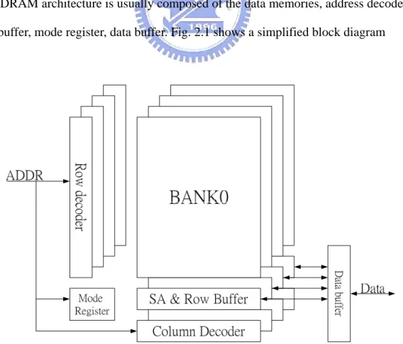
DRAM architecture is usually composed of the data memories, address decoders,
row buffer, mode register, data buffer. Fig. 2.1 shows a simplified block diagram
Four bank share the address bus and command bus. Each bank has its own row
decoder, column decoder, and sense amplifier. The mode register stores the DRAM
operation mode, including burst length (BL), column address strobe latency (CL), and
burst type, etc. Users can set the value of the mode register through address bus with
proper command.
2.1.2 DRAM command and operation
The normal commands and its operation used in DRAM will be introduced as
follow.
NO OPERATION (NOP):
The NOP command can prevent unwanted commands from being registered
during idle or wait states. Operations already in progress are not affected.
ACTIVE:
This command is used to open a row in a particular bank. The row remains open
for accesses until a PRECHARGE command is issued to that bank.
READ/WRITE:
The read/write command is used to initiate a read/write access to an active row,
if auto precharge is selected, the row being accessed will be closed at the end of read.
PRECHARGE:
The precharge command is used to deactivate the open row in a particular bamk.
The bank will be available for a subsequent row access a specified time (tRP)
REFRESH:
The refresh command can be used to retain data in the DRAM.
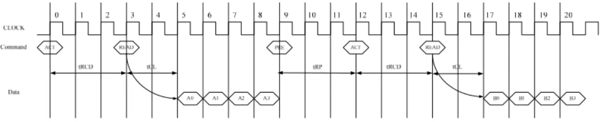
A memory access operation, which simplified state diagram is depicted in Fig.
Fig. 2.2 Bank state diagram.
The active command opens a particular row in one of the bank, and copies the
row data into the row buffer. The active command needs a latency period called tRCD
to accomplish this operation. Then, after tRCD delay a column access command (read
/ write) can be issued to sequential access data or single data according to the burst
length and burst type set in the mode register. During the tRCD time, no other
commands can be issued to the bank. However, commands to other banks are
permissible due to the parallel processing capability of each bank. For read operation
the valid data-out from the starting column address will be available following the
CAS latency after the read command, as shown in Fig. 2.3. For write command in
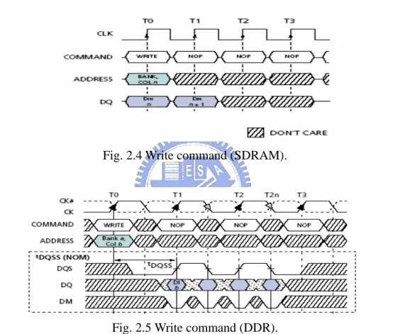
SDRAM, the first data-in is coincident with the write command, as shown in Fig. 2.4.
For write command in DDR DRAM, the first data-in is sent to DQ [1] strobe after a
DQS [1] delay, as shown in Fig. 2.5. Finally a precharge command must be issued
Fig. 2.3 Read command CAS latency.
Fig. 2.4 Write command (SDRAM).
Fig. 2.5 Write command (DDR).
2.2 Past DRAM controller techniques
In the design of system-on-a-chip such as portable wireless device and
multimedia system, several factor such as increased system complexity,
time-to-market pressure, cost effectiveness, and various functionality requirement
have made the trend of system-on-a-chip design indispensable. In general, SoC device
functional blocks. As the SoC integrate more functional block and need high
performance, high data bandwidth is required to meet a given system specification.
Similarly Because of the tremendous data transfer and storage in video process,
software or hardware must provide high data bandwidth to achieve the real-time
request in multimedia system. External memory has the largest data capacity so it is
often used as the frame memory in the video process. Nevertheless, the data transfer
to off-chip memory is bound to the limited bandwidth.
Many external memory controllers have been proposed to improve the memory
bandwidth utilization and achieve efficient memory access. In this section, some
important techniques used in memory controller will be introduced.
2.2.1 Techniques and Improvement
According to the environment, the controllers can be categorized into two classes:
single channel and multiple channel environments. For single channel environment,
Rixner memory access scheduler [2] reorder the access addresses from each bank
controller and sends command to DRAM through arbiter. It can reduce the latency
after reorder the address. However, the output command may be out-of-order, many
command FIFOs and extra circuits are required to reorder commands and addresses.
Miura dynamic-SDRAM-mode-control scheme [3] eliminates the above
disadvantage and it can both reduce operating current and the latency of an SDRAM.
Nevertheless, it only supports scheduling of single-channel. For multi-channel
environment, Lee advances a quality-aware memory controller [4]. It supports
different scheduling policies according to the current channel situation. These
Concerning the particular-purpose memory controllers for the video codec
application, several papers have been proposed on improvement of performance. They
focus on the power consumption, latency (speed), and bandwidth utilization.
Kim memory interface architecture [5] reorganizes data arrangement in SDRAM
The interface reduces energy consumption and increase memory bandwidth by
placing the data in the same block in the same row. Thus, when accessing the block,
the row-hit rate increases. The time and power waste on pre-charging the rows are
decreased. Fig. 2.6 (a) is the original placement, and Fig. 2.6 (b) is the new placement
after data arrangement.
Fig. 2.6 Data placement
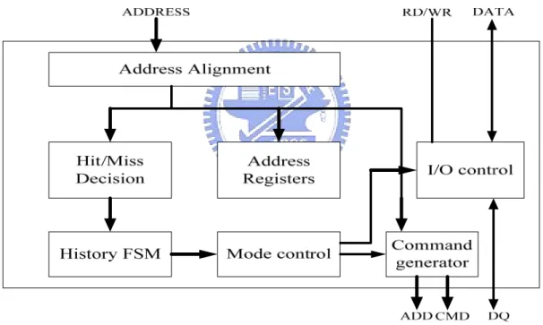
Park history-based memory mode control [6] reduce row-miss rate to achieve
23.3 % reduced energy consumption and 18.8 % reduced memory latency. It uses
history-based prediction to predict the next command is row-hit or row-miss. The
the current row stay in the active state if it predict the next command is row-hit. The
proposed memory controller is shown in Fig. 2.8.
Fig. 2.7 Mode control prediction
Fig. 2.8 Mode control memory controller
Zhu SDRAM controller in H.264 HDTV Decoder [7] focus on memory mapping
and data arrangement in SDRAM to reduce the row active cycle, it also improves
throughput and provide less power consumption. However, it adopts auto precharge
access latency.
Heithecker proposed a mixed QOS SDRAM controller [8]. The controller uses
two types of scheduler to do the memory access. It can improve the memory
bandwidth and latency for multiple access streams with different access sequence
types running in parallel. Fig. 2.9 shows the overall controller structure with two
scheduler variants.
Fig. 2.9 2-stage scheduler memory controller
Kang proposed a memory controller in the MPEG-4 AVC/H.264 decoder [9]. It
uses a dual memory controller and dual bus to improve the memory bandwidth
The above memory control technique concentrate on three part, including
memory scheduler, mode control, and data arrangement in SDRAM. The above
discussion of related controllers and its techniques is summarized in Table 2.1.
Besides the techniques mentioned above, there are still other techniques can
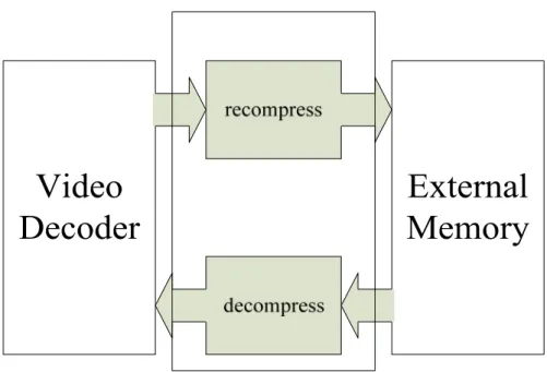
apply on the video process such as frame recompression and frame memory
reorganization. Frame recompression is recompressing data before storing to memory,
and decompression is required when reading data from memory, as shown in Fig.
Fig. 2.10 recompression method
In this respect, many algorithms, such as Tajime [10] 2-D adaptive DPCM in
pixel domain, and Lee [11] modified Hadamard transform and Golomb-Rice (GR)
coding, etc have been proposed. However, frame recompression method need extra
circuit and require additional execution cycles to compress data such that the
throughput of video decoder degrades. For the memory reorganization can be found in
De Greef [12]. Beside, Interuniversity MicroElectronic Center (IMEC) widely
exploited this idea to H.264 decoder system [13], MPEG-4 motion estimation [14]
and video decode [15]. The concept of memory hierarchy [16] combined with
merging structured frame memory can achieve data reuse and reduce the redundancy
if data access. However, they only focus on C level simulation. If we want implement
on ASIC design, many issues still have to be overcome. For advanced development,
Chang combined frame memory architecture [17] can reduce frame memory size up
Table 2.1 Related works of SDRAM memory controller
Related Application Improve Technique
Rixner General-purpose single-channel
Bandwidth
Latency
Memory schedule
Miura 32 bit RISC CPU
single channel STB
Latency
Power
Memory
mode control
Lee Multimedia SoC
multiple-channel STB Bandwidth Latency Memory schedule Kim Video single channel Power Bandwidth Data arrangement Park HDTV decoder Multiple-channel Latency power Memory mode control Zhu H.264 decoder Multiple-channel Bandwidth utilization Decoding throughput Data arrangement
Heither Image process
Multiple-channel Bandwidth utilization Latency schedule Kang H.264 decoder Multiple-channel Bandwidth utilization Dual controller
2.3 Modern DRAM Development
From the day DRAM has been invented, the requests of performance accelerate
very fast. The most important issues are bandwidth, latency, and power. This section
will introduce the development of DRAM that improve the performance and the
future trend of DRAM.
2.3.1 Bandwidth
The improvement of DRAM bandwidth has never satisfied the increasingly
complicated application such as multimedia and 3D processing. To fulfill the demand
for high bandwidth, various new DRAM specifications have been announced by
DRAM manufacturers. The SDRAM standards supported by JEDEC [18] have
become the mainstream of DRAM market. Several techniques have been applied on
the latest standards announced by JEDED to provide users higher bandwidth.
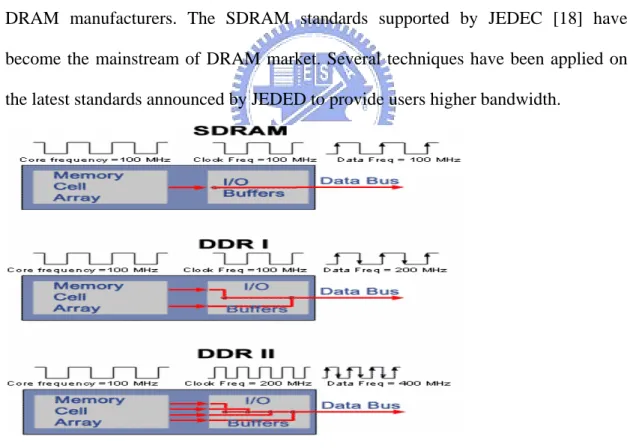
Fig. 2.11 Operating frequency of SDR, DDR-1, DDR-2
Fig. 2.11 shows the operating frequency of each component of SDR, DDR-1, and
DDR-2. As we can see, in SDR, the core and the I/O are running at the same
data PREFETCH technique is applied. Data is transferred at positive and negative
edge of clock. The data rate of DDR-1 is twice as SDR. In DDR-2, the PREFETCH
technique is further promoted up to 4-bit. The I/O frequency is twice as DDR-1, so
DDR-2 can provide bandwidth twice as DDR-1 can. The PREFETCH technique
makes DRAM be able to provide quadruple bandwidth than SDR with core frequency
remains unchanged.
In SDR and DDR-1, row activation takes a period of time called tRCD before
column access command can be issued. This may induce overhead due to the bus
confliction. For example, Fig. 2.12 shows the difference between DDR and DDR-2.
The top part is the timing diagram of DDR. Because of the bus confliction The third
active command can not be issued at 4th cycle. It must wait a cycle therefore make a
bubble on the data bus. The bottom part of Fig. 2.12 is the timing diagram of DDR-2.
DDR-2 allows users to issue subsequent read command right after an active command.
The read command will be buffered inside DDR-2 and will not be processed until the
tRCD latency is reached. Thus the bus confliction is prevented, the bubble is
eliminated and the bandwidth utilization becomes better.
2.3.2 Latency
The DRAM response latency can directly influence the speed of the whole
system. The speed of the system for the multimedia process is very essential to
achieve the real-time request. So if the DRAM latency is shorter, the whole system
can boost its performance. However, the situation is not as we expected. Fig. 2.13
compares the performance trend of CPU and DRAM. While CPU clock speed
increases 7.65 times, DRAM latency also has a 4.6 times increase. The improvement
of CPU is much faster than the improvement of DRAM. Long response latency waste
its processing power on waiting and the performance is limited.
Fig. 2.13 CPU VS DRAM performance
Since Year 2000, DRAM manufacturers have begun to pay attention to the
impact of DRAM latency and proposed several solution including RLDRAM (reduce
latency DRAM) [19], FCRAM (Fast cycle RAM) [20], and Network DRAM [21] etc.
In the following we will introduce RLDRAM for example.
RLDRAM-1 which mainly aimed at application requiring short latency and high
bandwidth was announced by micron in 2001. RLDRAM-2 was announced in 2003
and can be taken as an enhanced version of RLDRAM-1. Some features if
RLDRAM-2 are listed as followed.
banks. The successive accesses to the same bank cost more latency than the
successive accesses to the different banks, shows in Fig. 2.14 and Fig. 2.15. So if the
number of banks increases, the rate of accessing different banks increases. So the
latency of RLDRAM is shorter than the traditional DRAM. On the other hand, Row
cycle time (tRC) defined the shortest time interval needed for two successive ‘active’
commands addressed to the same bank. The row cycle time is 20ns in RLDRAM and
72ns in RDRAM respectively. When the row miss happens, RLDRAM can apparently
save much access latency.
RLDRAM has another advantage of saving latency. It separates data bus for read
and write data, RLDRAM-2 can effectively reduce the latency caused by the
turnaround cycles.
Fig. 2.14 Accesses addressed to same bank
2.3.3 Power
In many application of portable wireless devices such as mobile and PDA, power
consumption is the significant issue because of battery life is limited. With the
application of multimedia becomes popular, the request of memory size is larger.
Accordingly, the designers often select DRAM to be the body memory component.
In order to reduce the power of DRAM, many products have been invented for
low power such as BAT-RAM from micron [22] and Mobile-RAM from Infineon [23].
The low-power DRAM has some special features inside.
Low Operating voltage
Compare with SDR SDRAM, the operating voltage of low-power DRAM is
lowered from 3.3v to 1.8v. Thus, the power consumption can significantly decreases.
Output Driver Strength
Because the low-power DRAM is designed for use in smaller systems that are
typically point-to-point connection, an option to control the drive strength of the
output buffers is provided. Drive strength should be selected based on expected
loading of the memory bus. There are four allowable setting for the output drivers,
including full strength driver, half strength driver, quarter strength driver, and
one-eighth strength driver.
Temperature Compensated Self Refresh (TCSR)
Most of the time mobile devices stay in standby mode and DRAM can enter sef
refresh mode to save unnecessary power consumption. In the self-refresh mode,
DRAM will refresh the data stored in the DRAM cell. The refresh period is inversely
proportional to temperature, traditional DRAM can only support single refresh period
implemented for auto control of the self refresh oscillator on the device. Therefore,
the refresh current is decreasing while the temperature is low, as shown in table 2.2.
Table 2.2 Current of different condition
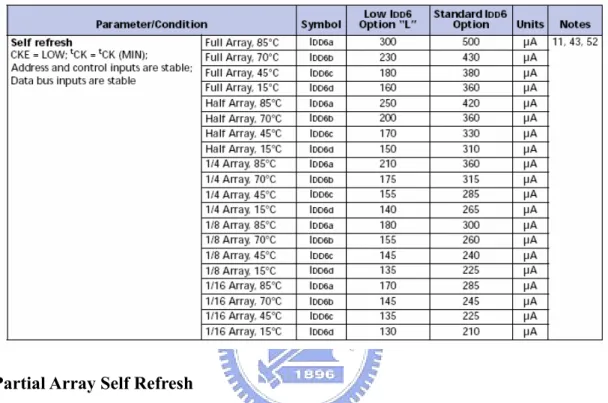
Partial Array Self Refresh
For further power savings during SELF REFRESH, the PASR feature enables the
control to select the amount of memory that will be refreshed during SELF REFRESH.
The option is shown in Table 2.3. The current can be reduced as shown in Table 2.1.
Stopping the external clock
One method of controlling the power efficiency in applications is to throttle the
clock that controls the SDRAM. There are two basic ways to control the clock:
1. Change the clock frequency, when the data transfers require a different rate of
speed.
2. Stopping the clock altogether.
Both of these are specific to the application and its requirements and both allow
power savings due to possible fewer transitions on the clock path.
The clock can also be stopped altogether if there are no data accesses in progress,
either WRITE or READ, that would be affected by this change; i.e., if a WRITE or a
READ is in progress, the entire data burst must be through the pipeline prior to
stopping the clock.
For the full duration of the clock stop mode. One clock cycle and at least one
NOP is required after the clock is restarted before a valid command can be issued. Fig.
2.16 illustrates the clock stop mode.
It is recommended that the DRAM be in a pre-charged state if any changes to the
clock frequency are expected. This will eliminate timing violations that may
otherwise occur during normal operations.
Power-Down
Power down can occurs when all banks idle, this mode is referred to as precharge
power-down. If power down occurs when there is a row active in the bank, this mode
is referred as active power-down. Entering power-down mode deactivates all input
and output buffers, therefore the power is saved.
Deep Power-Down
Deep power down is an operating mode used to achieve maximum power
reduction by eliminating the power of the memory array. Data will not be retained
when the device enters power-down mode. Since DRAM is often used as temporary
data buffers, enter DPD mode while the device is in standby mode won’t cause any
loss.
2.4 Future trend of DRAM
DDR-3
Beside DDR-2, the draft of DDR-3 industry standard has been announced by
JEDEC in Oct 2002. DDR-3 SDRAM which is due to enter volume production in
2006, operates from a 1.5 volts supply and can transfer data at up to 1,066-Mbits per
second. That's twice as fast as DDR2, which is just coming into the market in volume,
and four times the speed of DDR. Samsung said it plans to make the chips using an 80
nanometer manufacturing process and, citing data from research house IDC, believes
DDR3 has some features that can improve the performance and more
cost-effective [24]. In the 8b-prefetch data-path with 3-stage pipelining, a newly
devised hybrid-type latency control scheme and a 2-step multiplexing can proficiently
handle maximum 128b parallel data in the case of x16 configuration. An efficient
protocol for the temperature read-out is proposed, supporting CPU while it controls
the heat in high-speed operations. Per-bank-refresh is another experimental feature of
this prototype, virtually removing the loss of the memory bandwidth due to the
unavoidable requirement of refresh operation common in all DRAM.
Embedded DRAM
Embedded DRAM (EDRAM) technology has significant advantage in terms of
performance, area, bandwidth, and power consumption by combining a high
bandwidth DRAM macro with logic/analog circuits on the same chip.
Embedded DRAM (EDRAM) macros have been proposed as a way to achieve
the low power and wide bandwidth required by graphic controllers, network systems,
and mobile systems. To give an example; Advanced 3D graphics (3DG) technology
will be used in console game machines [25], and it is desired to develop a rendering
controller chip which can handle real time 3D animation with true colors. Embedded
DRAM (EDRAM) [25] technology attracts attention of the 3DG systems, because
only EDRAM can satisfy the required data rate. Fig 2.17 shows the trend of 3DG
controller performance.
In the portable device such as mobile and PDA, the power consumption is a very
important issue. In off-chip design, the power consumption of off-chip
interconnection is larger one or two orders of magnitude than that of standalone
on-chip interconnection is reduced to the same order of that of EDRAM because
on-chip I/O capacitance is tremendously reduced. Therefore the power consumption
of connection can be saved.
Although embedded DRAM technology has significant advantage in SOC design
because of its performance such as low-power consumption and high bandwidth.
However, process gap between commodity DRAM and logic make it difficulty to
make highly reliable EDRAM product with low cost, and high yield. There are still
other problems need to overcome in the design of EDRAM. But the implementation
of EDRAM technology would be a trend in the design of SOC.
Chapter 3
Transaction Level Modeling of
H.264/AVC Decoder
The proposed controller is designed for the video process which need large
amount of data storage. We have a project to design a hardware architecture for the
H.264 decoder that confirms to high profile at Level 4 (HP@L4). As a result of the
complexity of the H.264 decoder, it needs a memory controller to communicate with
external memory efficiently. We have a cooperation to integrate my memory
controller into the H.264 decoder system design. The characteristic of H.264 and the
system design of this H.264 decoder will be introduced in this chapter. The role of my
memory control in this H.264 decoder system will also be described here.
3.1 Overview of H.264
3.1.1 Introduction
H.264/AVC is the newest international video coding standard. Relative to prior
video coding methods such as MPEG-2 video, H.264/AVC has the higher coding
efficiency. With an increasing number of services and growing popularity of high
definition TV are creating greater needs for higher coding efficiency. Moreover, other
transmission media such as Cable Modem, XDSL, or UMTS offer much lower data
rates than broadcast channels, and enhanced coding efficiency can enable the
existing digital transmission capacities.
The scope of the standardization is illustrated in Fig. 3.1, which shows the
typical video coding/decoding chain (excluding the transport or storage of the video
signal). Only the central decoder is standardized. By imposing restrictions on the
bit-stream and syntax, and defining the decoding process of the syntax elements such
that every decoder conforming to the standard will produce similar output when given
an encoded bit-stream that conforms to the constraints of the standard.
The new standard is designed for many application areas such as the following
example.
• Broadcast over cable, satellite, cable modem, DSL, terrestrial, etc.
• Interactive or serial storage on optical and magnetic devices, DVD, etc.
•Conversational services over ISDN, Ethernet, LAN, DSL, wireless and mobile
networks, modems, etc.
• Video-on-demand or multimedia streaming services over ISDN, cable modem, DSL,
LAN, wireless networks, etc.
• Multimedia messaging services (MMS) over ISDN, DSL, LAN, wireless and mobile
networks, etc.
3.1.2 Characteristic of H.264
The coding gain of H.264 is achieved by efficiently exploiting spatial and
temporal redundancy. For better temporal prediction, new coding tools such as
long-term prediction, multiple reference frames, motion compensation with variable
block size, in-loop filter, and 1/4-pel motion compensation are developed. In addition,
for exploiting spatial redundancy, an intra prediction technique is adopted. Further, to
reduce bit rate, a context-adaptive entropy coder is deployed. The following briefly
summarizes the features of each coding tool.
• Long-Term Prediction: The prediction of a picture can refer to a prior coded picture that is not right before the current one. For sequences with periodic content,
long-term prediction offers coding gain by having more flexibility on the selection of
reference picture.
• Motion Compensation with Variable Block Size and Multiple Reference
Frames: Motion compensation can be done by partitioning a macroblock into a few
number of sub-blocks and each sub-block can refer to a larger number of pictures that
have been coded and stored. The features of variable block size and multiple reference
frames offer better trade-off between texture and motion information as well as better
adaptation for macroblocks with varying characteristics.
• 1/4-pel and 1/8-pel Motion Compensation: The prediction can come from 1/4-pel samples (or 1/8-pel for chroma) that are generated by using the interpolation with
full-pel samples as input. The sub-pel motion compensation with higher accuracy
improves the prediction efficiency by reducing the aliasing from sampling.
• Intra Prediction: An intra-coded block can be predicted from the edges of the adjacent and previously-coded blocks. Particularly, the prediction can come from
different directions.
• Transform with Variable Block Size: The 4x4 integer transform and 8x8 DCT transform can be adaptively selected for a macroblock. The 4x4 integer transform can
remove ringing artifact while the 8x8 DCT provides higher coding efficiency for
smooth area. In addition, a double transform could be applied for the DC coefficients
belonging to the 16 4x4 blocks within a macroblock.
• Context-Adaptive Entropy Coding: The entropy coding is done in a context-adaptive manner. The value of prior coded syntax elements (or bins) could be
used to select the probability model or table for the coding of following syntax
elements (or bins). Higher coding efficiency is achieved by using conditional
probability models.
• In-loop De-Blocking Filter: A de-blocking filter is placed in the prediction loop to remove the blocking artifact for the reference picture so as to improve the quality of
the reference picture and prediction efficiency.
While more correlations are used for coding, it suggests that stronger data
dependency exhibit between successive computations and more buffers are required.
Moreover, the very different types of predictors imply that intensive computations are
inevitable. Also, the heterogeneous building blocks and operations bring new
challenges to a system design such as synchronization, data flow control, error
handling, buffering, software/hardware concurrency, and so on. With these design
challenges, the SoC implementation for H.264 codec becomes much more difficult
than prior coding standards. Due to the complexity of H.264, a proper top-level
regression would be time-consuming and the loss of cost is significant if the system
architecture has any errors. The following introduces a new SoC design philosophy,
transaction level modeling, which allows us to explore the design spaces at system
level by providing trade-off between implementation details and simulation accuracy.
3.2 Transaction Level Modeling
3.2.1 Introduction of TLM
As described in the previous section, the traditional design methodology can not
satisfy the need for the design of complex system. The reason is that many
unnecessary implementation details are captured for the system-level modeling. Thus,
the simulation speed could be so slow that the verification at system level may not be
done thoroughly. Recently, a modeling technique called transaction level modeling
(TLM) is proposed to achieve the system-level modeling. The idea is to make another
level of abstraction between the system specification and its RTL implementation so
that unnecessary implementation details can be hid from the system-level modeling.
As far as the system is concerned, the implementation details for each component is
not the most important in the early development phase. Instead, the system parameters,
such as the partition of the tasks, the functionality of each component, the topology
that connects different components, the communication protocol between components,
the memory hierarchy, and so on, are of more interest.
There are four types of TLM including (1) the PE-assembly model, (2) the
bus-arbitration model, (3) the cycle-accurate computation model, and (4) the
timing-accurate communication model.
level is the specification model and the bottom level is the implementation model. The
marked level between specification model and implementation model are transaction
levels. According to the modeling accuracy in computation and communication, each
model represents an operating point in Fig. 3.2 (b), where the bottom-left corner
stands for the specification of the system while the top-right corner denotes the
detailed implementation at register-transfer level. Particularly, only the four modules,
PE-assembly model, bus-arbitration model, time-accurate communication model, and
cycle-accurate computation model, are considered as the TLM.
specification model PE-assembly model Bu s-arbitration model Time-accurate communication model Cycle-accurate computation model Implementation model More Accurate Computation C o m m u n icat io n More Accurate Un-Timed Un-Timed Approxiate -Timed Approxiate -Timed Cycle-Timed Cycle-Timed SM TLM TLM TLM TLM RTL (1) (2) (3) (4) (1) (2) (3) (4)
(a)
(b)
Fig. 3.2 System model at different levels of abstraction
Table 3.1 indicates the characteristics of different system models. As shown,
different models capture different degrees of accuracy in computation and
communication. The specification model and the implementation model represent the
The models in between are the four types of TLM, which offers the flexibility on
selecting the simulation accuracy and speed.
Table 3.1 Characteristics of different models
Models communication time computation time
communicatoin
schene PE interface
added Implementation detail
Specificaton model no no variable (no PE)
-PE-assembly model no approximate message-passing
channel abstract
PE allocation, process PE mapping
Bus-transaction model approximate approximate abstract bus
channel abstract
bus topology, bus arbitration
Time-accurate
communication model time/cycle accurate approximate
detailed bus
channel abstract detailed bus protocol
Cycle-accurate
computation model approximate cycle accurate
abstract bus
channel pin accurate RTL/ISS PEs
Implementation model cycle accurate cycle accurate wire pin accurate detailed bus protocol or RTL/ISSPEs
3.2.2 Design flow with TLM
Traditional design flow can not ensure the quality of the design when the system
complexity increases dramatically. This section presents a new SoC design flow with
TLM as the platform for concurrent software and hardware development. The new
design flow mainly comprises two parts, which are (1) the new system-to-RTL
extension and (2) the traditional RTL-to-layout flow. The first part is different from
Requirement Definition Specification Development
Specification Model
System Architecture and TLM Development TLM RTL HW Refinement SW Design and Development HW Verification Environment Development
Fig. 3.3 Design floe with transaction level modeling
Fig. 3.3 indicates the new system-to-RTL extension. As shown, after the
specification is defined, the system architecture is developed and verified by using
TLM. Upon the completeness of the TLM model, it is used as a unique reference to
both software and hardware teams. For the software team, the embedded software is
developed and verified based on the TLM model. For the hardware team, the TLM
serves as the golden model for the detailed implementation. Along with the
development of software and hardware, the TLM model can be annotated with more
accurate timing information. Consequentially, not only the functionality but also the
timing can be verified together. Differs from the traditional design flow, the new
is the key for ensuring the quality of the design. The following summarizes the
functionality of TLM in the SoC design flow:
1. Verification model for design space exploration.
2. Platform for early software development.
3. Specification and golden model for hardware development.
Nowadays, EDA tools are still not capable of automatically converting TLM to
detailed hardware implementation. The hardware refinement is still done through a
traditional paper specification and RTL coding. TLM appears to be an extra workload
and unnecessary task. However, it still brings many benefits that significantly reduce
the time to market:
1. System integration at the early stages so that the potential problems can be found
and solved earlier.
2. Faster simulation speed while maintaining the accuracy of simulation.
3. Concurrent software and hardware development.
4. Platform for software/hardware co-design and co-verification.
5. Incremental hardware refinement and implementation details by means of hybrid
abstraction level modeling.
For the implementation of TLM, we present the System C library. In the System
C, there are 3 major components, which are process, channel, and interface function.
The processes define the operations of a component and can be triggered by a set of
predefined events. In addition, the channel specifies the connections among different
components and the interface function provides the means for a component to
communicate with the others. Within a component, the processes can call the interface
interface functions. Consequentially, by well defining the interface functions, the
communication part and the computation part can be developed and refined
independently.
Due to the benefits of the TLM, it will become a critical step in the SoC design
flow. In the next section, the system architecture of our H.264 video decoder that is
designed by using will be introduced.
3.3 Transaction Level Modeling of H.264 Decoder
In most video coding standard, different profile level will support different
coding tools such as transform8x8, supporting frame size, and MBAFF. As a result,
the profile level definition is very important to the complexity and cost of the overall
system architecture. This section will describe the profile level of our H.264 decoder
first. The system architecture designed in TLM model will be introduced next.
3.3.1 Specification
In H.264 standard, there are many different profile levels which contain different
coding tools to improve the coding efficiency. Thus, different decoder design
supporting for differnet profile will be different in performance and cost. This section
presents a design specification of decoder conforming to high profile at level 4. Any
bit-streams conforming to main/high profile with a level lower than or equal to 4 shall
be decoded. Specifically, the decoder supports the decoding throughput up to
1920x1080i@60Hz. In the following, some properties of high profile and level limits are listed.
2. No data partition.
3. Arbitrary slice order is not allowed.
4. No slice group and no redundant picture.
5. chroma_format_idc in the range of 0 to 1.
6. bit_depth_luma_minus8/bit_depth_chroma_minus8 equal to 0 only.
7. qpprime_y_zero_transform_bypass_flag equal to 0 only.
8. Up to 16 reference frames. (32 reference fields).
9. Vertical motion vector range does not exceed MaxVmvR as in Table 3.1.
10. Horizontal motion vector range does not exceed the range of -2048 to 2047.75
11. Up to 32MVs perMB.
12. Number of bits per macroblock is not greater than 3200.
Moreover, Table 3.2 shows more constraints of different profiles. With
summarizing these profile limits, we can start to design our micro-architecture of
H.264 decoder to satisfy all functionalities while minimizing the cost.
3.3.2 System Architecture of H.264 decoder
Fig. 3.4 shows the overall architecture of this system, which is developed based
on the ARM platform. For the chip I/O, the compressed bit-stream is input via a
hardware interface, which communicates with the host by a bridge, and the decoded
frames are output to the monitor via HDMI interface. The reference pictures, decoded
pictures, and motion vectors for each reference picture are stored in the external
memory. All the data access to external memory will go through the memory
controller.
32-bit AHB Control Bus
Memory Controller S SDRAM 0 CABAC CAVLC S
128-bit AHB Data Bus
Bit-stream FIFO ARM 9 CPU M Instruction Memory Data Memory IQ/IDCT S MB Texture Buffer MB Motion Buffer Data Fetch S Intra/Inter Prediction S Subblock Reconstruct Buffer DeBlocking S,M IIP FIFO DB FIFO DeInterlacer S,M DI FIFO
SDRAM 1 SDRAM 2 SDRAM 3
Harddware Input Interface
M,M Sync FIFO HDMI Interface S u b b l o c k P r o c e s s i n g U n i t NAL Parsing
Fig. 3.4 System architecture diagram
Inside the chip, there is an embedded CPU and two AHB buses, which are
data bus is used by Data Fetch, De-blocking and De-interlacer for data transfer
between these modules and external memory. In addition to the AHB buses, there are
backdoor-to-backdoor connections between modules. The modules connected by
backdoor channel make up a video pipe, where its input comes from bit-stream FIFO
and its output is drive to the HDMI interface. Particularly, the data between modules
are exchanged on block by block basis with block size being 8x8 except for CABAC.
In this system, the headers of sequence, picture, and slice are parsed by CPU.
The data below slice level are processed in the video pipe. According to the
information in sequence, picture, and slice headers, CPU can configure the modules in
the video pipe through the control bus for various decoding modes. Each module can
also be independently tested by CPU. The following briefly describes our video pipe
and system schedule.
3.3.2.1 Video Pipe
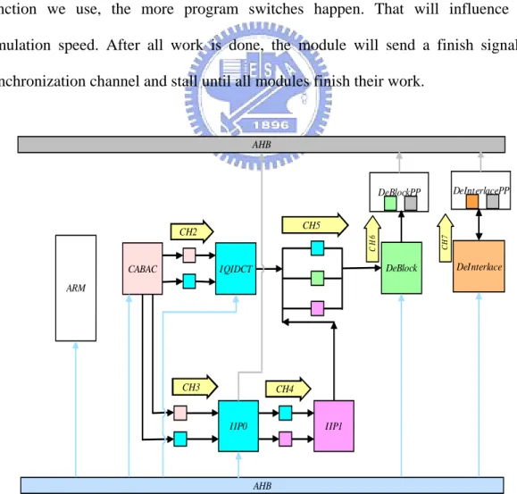
In our H.264 decoder, our video pipe contains seven modules which are CABAC,
IQ/IDCT, Data Fetch (DF), Intra-Inter prediction (IIP), De-Blocking, and
De-Interlacer. CABAC is the first module in video pipe and the functionality of
CABAC is decoding the bit-stream syntax below slice header. Because our decoder
processes luma and chroma components in parallel and CABAC can not decode
chroma components until all luma coefficients have decoded in one macroblock, it is
more efficient to make CABAC operate in macroblock level. For saving the buffer
size, all other modules operate in 8x8 block.
After CABAC the pipeline process to IQ/IDCT module and DF module. The
IQ/IDCT module does the inverse quantization and inverse discrete cosine transform
reference block for Inter block and intra prediction type decoding for Intra block.
Following after the DF is IIP which produces the value of prediction block for Intra
and inter prediction and adds the results with the residuals from IQ/IDCT. Because we
let IQ/IDCT start earlier one eight by eight block than IIP, it can make sure that IIP
always has the corresponding residuals.
After that, de-blocking is performed for reducing the blocking effect. For
keeping the data order correct, there are three eight by eight block buffers between
IQ/IDCT, IIP, and De-Block. For example, when IQ/IDCT is writing the third buffer
and IIP is writing the second buffer, De-Block is reading the first block buffer. In
addition, because de-blocking has specific process order in macroblock level but our
process unit is eight by eight block, we must change the process order shown in
Figure 3.2 but still keep the rule in specification. In Figure 3.2, the number means the
process order in one block. Fig. 3.5 present the eight by eight block order in zig-zag
scan of one macroblock.
3
1
5
6
2
4
2
1
5
3
8
4
6
9
7
10
3
4
1
2
5
6
4
8
1
2
5
3
6
9
7
10
Fig. 3.5 De-blocking process order
The last module is De-Interlacer which will work only when the source sequence
is field. The functionality of De-Interlacer is to translate a field picture to a frame
picture. Because the algorithm of De-Interlacer will use the previous, current, and
next one field in display order, it will also cost bus bandwidth. Besides, the fields for
size of external memory to store the data.
3.3.2.2 System Schedule
Without a system schedule to control data flow in video pipe, it is possible that
the functionality of whole system is wrong even if every module is well verified. This
section describes briefly our system schedule shown in Table 3.3. In the beginning of
decoding, we need an initial period to decoding bit-stream above slice header and to
set the control registers of every hardware modules by ARM CPU. After that, all
hardware modules start to decode one by one. When CABAC starts to decode the
second macroblock in current slice, the first macroblock is fed into the following
modules in eight by eight block unit. As a result, IQ/IDCT and DF, IIP, and DeBlock
process the different eight plus eight block.
During the slice changes, the CPU will detect the NAL unit first and start to
decode the slice header. When CPU is decoding the slice, the hardware may stall
depending on the time the NAL unit is detected, slice header decoding speed of CPU,
and block decoding speed of hardware modules. Table 3.3 shows the condition that
hardware modules will stall. In addition, when the picture changes, there is same
condition as slice.
Looking into the hardware pipe, every module has different process time. As a
result, when a module finish current block, it does not mean that the module can
process next block right now because the input data may be not ready and it may over
write the data which next stage is using. In our decoder design, if one module is
finished, it will not start again until all hardware modules are finished. Thus, for
supporting real-time decoding, all modules must make sure that they can finish their
3.3.2.3 System Modeling
For transaction design at transaction level, Fig. 3.6 shows the concept about how
we implement all modules with sc_thread. First, we define the input and output ports
connecting with other modules. All data transmission is through channel by calling
the interface functions of ports. In the program part, the module will read input data
through input channel in the beginning. Then, the finite state machine decides which
path th program will go through. In the main program, the functionality can be
composed of one or more functions and we can decide to use wait function after the
end of every function or only use once after all functions are finished. The more wait
function we use, the more program switches happen. That will influence the
simulation speed. After all work is done, the module will send a finish signal to
synchronization channel and stall until all modules finish their work.
DeBlockPP CABAC IQIDCT IIP0 IIP1 DeBlock DeInterlace AHB AHB DeInterlacePP CH2 CH3 CH4 CH5 CH 6 CH 7 ARM
3.4 Memory Controller in H.264 Decoder
There are three main modules in the H.264 decoder will access external memory
to receive or give data. These three modules are inter prediction (motion
compensation) module, de-blocking module, and de-interlace module. The
relationship between these modules and external memory is shown in Fig. 3.7.
AMBA BUS M emory Controller BUFFE R Inter block(MC ) BUFFE R De-block BUFFE R De-interlace DRAM pad
External memory
Fig. 3.7 Relationship between H.264 decider and external memory
The functionality of de-block module is writing the re-construct block into the
external memory, all the decoded block will be stored in the external memory through
de-blocking module.
The inter prediction module is used to do the motion compensation for the
inter-block. The data fetch module obtains the motion vectors from CABAC block
first-in-first-out (FIFO) buffer before entering the inter prediction module.
In order to display the picture in field mode, a de-interlace module is need to
read the decoded field stored in the external memory and de-interlace the fields.
The H.264 decoder needs a memory controller to communicate with external
memory. Due the complexity of H.264/AVC decoder at level 4 we need a memory
controller that not only keep the correctness of data but also can help the whole
system to achieve better performance.
Fig. 3.8 Architecture of the memory controller in H.264 decoder
Fig. 3.8 shows the architecture of my memory controller inside the H.264
decoder. This memory controller combines two layers together. The Layer 0 is the
external memory interface (EMI) which is used to control the external memory. The
decoder. The Layer 0 part (EMI) will receive the addresses translated from Layer 1
(ATM) part and generate the appropriate commands to external memory.
The purpose of layer 0 (EMI) is to communicate with external memory. The EMI
is designed for various kind of system. As a result, the EMI is independent of the
system but dependent of the external memory. In order to make this EMI can fit
variable type of external memory. The configurability of this EMI is very essential.
The detail of EMI will be introduced in the Chapter 4.
Layer 1 is an address translation machine (ATM). It exploits the characteristics
of the video process to make the accesses become more regular. The Layer 1 is
designed for the memory subsystem. The detail of Layer 1 and the relationship
Chapter 4
External Memory Interface
In the design of SOC system, it usually needs an off-chip memory to storage the
large amount of data. The external memory interface is used to communicate with the
external memory for the system as shown in Fig. 4.1. To deal with tremendous data
transfer and storage in H.264 decoder, the external memory must provide high data
bandwidth to achieve the real time request. The bandwidth of the external memory is
limited due to the pin number of I/O is finite. Accordingly the external memory
interface must provide high data bandwidth utilization by using some techniques. The
proposed external memory interface will be introduced in this chapter.
4.1 Concept of EMI
The external memory interface (EMI) is one of the Layers in this memory
controller, that is, layer 0. EMI will receive the physical addresses from the address
translation machine or the functional block, and use the addresses to access the
DRAM. This external memory interface is designed to control the external memory,
and it will directly connect to the DRAM as show in Fig. 4.2.
Address & Write
data Layer 0 : EMI
Addr/cmd
DRAM
Data
Fig. 4.2 Connection of EMI
The external memory interface will generate the appropriate commands to
external memory (DRAM). The external memory can only accept the commands that
it defined in the specification, and the commands have been introduced in chapter2.
The design of my EMI is configurable for different kinds for external memory.
Users only have to set the specific parameter of the external memory that they use,
and this EMI will translate the accesses into the commands. Thus the users can
conveniently use this EMI to access the external memory (DRAM).
restriction on the design of SOC. In order to increase the performance of the whole
system this EMI is designed to achieve higher performance. The whole architecture
will be introduced in next section.
4.2 Architecture of EMI
The detail architecture is shown in Fig. 4.3. It contains five fundamental parts
inside the EMI. The input data and address will stored in the FIFO and generate the
appropriate command through the mode control block and the FSM block. Then the
commands will be send to DRAM. The detail of these parts will be described in the
following. Command FIFO W-Data FIFO (BA,ROW,COL,BL) Write Data (BA,ROW.COL,BL)
FSM
WRITE Data Mode control TimingChecker NOP Counter
Command DRA M INTE RFA CE
External
Memory
ADDR DATA WRITE Data Scheduler R-Data FIFORead data Data